Available online: https://edupediapublications.org/journals/index.php/IJR/ P a g e | 3737
SRAM Architecture with A Full-Swing Local Bitline Based on the
22-nm Fin FET Technology
Shaik Rubia &
P.Annapurna Bai
1 M. Tech Student, Dept of ECE, CRIT, Affiliated to JNTUA, AP, India .
2Assistant Professor, Dept of ECE, CRIT, Affiliated to JNTUA, AP, India
Abstract: In this paper, the drawback of the average-8T SRAM architecture based on an advanced technology is analyzed, and a suitable SRAM architecture that
overcomes this drawback is proposed. However, in the
case of anaverage-8T SRAM based on an advanced technology, such as a 22-nm FinFET technology, where the variation in threshold voltage is large, the boosted WL voltage cannot be used, because it degrades the read stability of the SRAM. Thus, a full-swing local BL cannot be achieved, and the gate of the read buffer cannot be driven by the full supply voltage (VDD), resulting in a considerably large read delay. To overcome the above disadvantage, in this paper, a differential SRAM architecture with a full-swing local BL is proposed. In the proposed SRAM architecture, full swing of the local BL is ensured by the use of cross-coupled pMOSs, and the gate of the read buffer is driven by a fullVDD, without the need for the boosted WL voltage. Various configurations of the proposed SRAM architecture, which stores multiple bits, are analyzed in terms of the minimum operating voltage and area per bit. It should be noted that the proposed differential SRAM architecture can resolve the half-select issue without the need for a write-back scheme, and it exhibits a competitive area; it also exhibits a full-swing local bitline (BL) that enables a considerably smaller read delay than that of average-8T SRAM architecture.
Keywords: Bit-interleaving, FinFET, low-voltage operation, static random access memory (SRAM)..
I. eINTRODUCTION
From last 5 decades we are scaling down CMOS devices to achieve the better performance in term of speed power dissipation ,size and reliability .Variability has become
increasingly troubling as the SRAM cell size is reduced ,such as short channel effect ,higher DIBL, poor sub threshold swing collectively known as SCE.
While technology scaling has made it possible to put more and more transistors on to a simple chip while at the same time allowing them to run ever faster, less simple effects are starting to show. Continuously shrinking of the device size comes with serious constraint on memory design like power consumption and stability. The device variation and leakage are increasing as the miniaturization of the transistor continues which also affects the reliability and performance of the device. Scaling of MOSFET dimensions and power supply imposes.
The Fin type MOSFET(FinFET)is one of the most desired device to scaled CMOS device. To solve this problem 3-D device structure could be a solution . In the FinFET short channel effects are suppressed by a thin body instead of channel dopants.
The 8T FinFET SRAM is shown in fig 2 . the 8T SRAM is similar to 6T with addional 2 transistors to decoupled separate read and write operation . in 6T SRAM during read operation there is potential stability problem . To overcome the problem of data storage destruction during the read operation an 8T SRAM is implemented, for which separate read/write line are used.
Available online: https://edupediapublications.org/journals/index.php/IJR/ P a g e | 3738 to be weaker than Pass Gate transistors (this constraint is
called write ability), and pull down (PD) transistors have to be stronger than Pass Gate transistors (readability). A write operation in SRAM is typically carried out at a WL voltage of VDD. In some cases, WL voltage can be lowered during the cell. In this paper 8T FinFET SRAM cell design and read/write operation has been studies using Visual TCAD simulation
(a)
Fig. 2. (a) Average-8T SRAM architecture and (b) its operational waveform.
II. RELATED WORK
“Reduction of leakage power in 8T SRAM cell using virtual ground,” This paper describes stability problems in 6T SRAM cell and their solutions with 8T SRAM cell. 8T SRAM with the virtual ground concept has been proposed which reduces leakage power. Comparison of 8T SRAM cell proposed with conventional 6T SRAM cell with respect to leakage power are proved by simulation and experimentally using the tool cadence (180nm technology).
“Design and Verification of Low Power SRAM using 8T SRAM Cell Approach,” SRAM cell stability will be a
primary concern for future technologies due to variability and decreasing power supply voltages. Advances in chip designing have made possible the design of chips at high integration and fast performance. Lowering power consumption and increasing noise margin have become two central topics in every state of SRAM designs.The Conventional 6T SRAM cell is very much prone to noise during read operation. To overcome the read SNM problem in 6T SRAM cell, researchers have considered different configurations for SRAM cells such as 8T, 9T, 10T etc. bitcell design. These designs can improve the cell stability but suffer from bitline leakage noise. This paper targets reduction of power consumption and evaluates the static noise margin of 8T SRAM bitcells. In this paper, we propose a novel 8T SRAM topology that achieves both cell stability and also reduces Power Consumption. With the proposed 8T SRAM circuit, the Read Static Noise Margin is nearly twice that of the Conventional 6T SRAM Cell.
“A 5.61 pJ, 16 kb 9T SRAM with Single-ended Equalized Bitlines and Fast Local Write-back for Cell Stability Improvement,” A 5.61 pJ, 16 kb 9T SRAM is implemented in 65nm CMOS technology. A single-ended equalized bitline scheme is proposed to improve both read bitline voltage swing and sensing timing window. A fast local write-back allows the half-select-free write operation without performance degradation. The test chip shows a minimum operating voltage of 0.24V and a minimum energy of 5.61pJ at 0.3V.
Available online: https://edupediapublications.org/journals/index.php/IJR/ P a g e | 3739 strength of the read buffer, and to eliminate read failures.
Leakage currents through the unselected cells during a read operation is addressed by boosting the footer virtual VSS (VVSS) of the read port to the supply voltage (VDD). To reduce the power consumption of instruction memories in battery-less SoCs, two features were utilized in this array: a read burst mode is used when reading consecutive addresses to reduce the read energy, and instructions with higher percentages of “1” data are defined since reading a “1” is less costly than reading a “0” in 8T cells. The proposed array can operate at a wide range of supply voltages (350–700 mV) and has two ULP modes: standby with retention (1.5 pW/bit) and shutdown without retention (0.13 pW/bit). Aggressive power gating of all peripherals during the standby state reduces the array power consumption down to 12.29 nW/KB at 320 mV with data retention. Compared to previously published 8T arrays, the proposed design provides the lowest standby power. The complete shutdown of the array allows further reduction down to 1.09 nW/KB and is suitable for reducing the power consumption of data memories in battery-less SoCs. The measured results from a commercial 130 nm chip show that the proposed array consumes a minimum of 6.24 pJ/access with a 17.16 nW standby power at 400 mV. The read burst mode allows up to 22% reduction in energy/access at 400 mV.
III. EXISTING SYSTEM
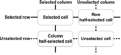
Several SRAM cell alternatives with a decoupled read port have been proposed for a low-voltage operation. The advantage of adding a decoupled read port is that it eliminates the tradeoff between the read stability and the write ability in the SRAM array to which the bit-interleaving is not applied; thus, the read stability and write ability can be optimized separately, facilitating a low-voltage operation. An SRAM cell is also susceptible to soft errors induced by α-particles; to address these errors, it is necessary for the SRAM array to exhibit bit-interleaving. Fig. 3 shows a bit-interleaved SRAM array architecture. In a bit-interleaved SRAM array, the selected cells are the SRAM cells targeted for the read or write operation. The row half-selected cells are the
SRAM cells located on the selected row and the unselected column, whereas the column half-selected cells are the SRAM cells located on the unselected row and the selected column. During the write operation, the row half-selected cells are disturbed because of the selection of the wordline (WL) of the row half-selected cells. Thus, the stability of the row half-selected cells should also be considered in the SRAM design.
Figure 3: Selected, half-selected, and unselected cells in a bit-interleaved SRAM array
Disadvantages
Power consumption is high Operating voltage is high
IV. Proposed System
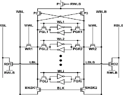
Available online: https://edupediapublications.org/journals/index.php/IJR/ P a g e | 3740 Fig. 4. Proposed SRAM architecture that stores i bits in one
block
The architecture of the proposed SRAM is verified. The characteristics of this model are fitted to those of a commercial low-power device based on the 22-nm Fin FET technology. Table I lists the technology parameters. For a statistical analysis, it is assumed that the variation in Vth of each transistor follows a Gaussian distribution, whose standard deviation (σVth)is expressed by
(a)
(b)
Fig. 7. Dynamic read noise margins of proposed SRAM at different PVT corners.
Read Operation
The read operation of the proposed SRAM architecture is described in Fig. 5(a). This operation is performed in two phases. During the first phase, BLK of the selected block is forced to remain at 0 V, and the selected WL is enabled. On the basis of the stored data, although the voltage of the LBL that is connected to the 1 storage node becomes high, its value cannot be as high as that of the full VDD because of the Vth drop through the pass gate transistor, and the voltage of the other LBL remains low. The read operation in the first phase is similar to that of the average-8T SRAM, except that the RBL is not discharged because the RWLB is high in the first phase. With the assertion of WL, although the 1 storage node is disturbed, the read disturbance is small because of the small capacitance at the LBL. This smaller read disturbance makes the proposed SRAM be able to operate in significantly lower operating voltage compared with 6T SRAM cell. The second phase starts with the falling of the RWLB. The assertion of the RWLB enables not only the discharge of the RBL but also the feedback of cross-coupled pMOSs. Positive feedback of the cross-cross-coupled pMOSs increases the LBL to the value of the fullVDD, owing to which the LBL can achieve a full swing, and the gate of the read buffer is driven by the full VDD, without the need for a boosted WL voltage. Thus, in the case of the proposed SRAM based on an advanced technology, the suppressed WL voltage can be used to enhance the read stability, without degrading the read delay. In other words, the advantage of the proposed SRAM architecture is that it eliminates the tradeoff between the read stability and the read delay.
Available online: https://edupediapublications.org/journals/index.php/IJR/ P a g e | 3741 Fig 5(b). Read operational waveform of SRAM architecture.
Write Operation
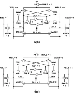
The write operation of the proposed SRAM architecture is shown in Fig. 6. As shown in this figure, BLK of the selected block is forced to remain at 0 V, and the selected WL is enabled. Further, the WWL is forced to remain at VDD so that the write access transistors are turned ON, and the WBLs are forced to remain at a certain voltage level on the basis of the write data. Both the storage nodes are connected to the WBLs through pass gate transistors and write access transistors. Thus, the write operation is differential, and the write ability of the proposed SRAM is better than that of the average-8T SRAM, whose write operation is single-ended.
6(a)
6(b)
6(c)
Fig. 6. (a) Selected, (b) row selected, and (c) column half-selected blocks of proposed SRAM architecture during write operation.
V. SIMULATION RESULTS
Available online: https://edupediapublications.org/journals/index.php/IJR/ P a g e | 3742
Figure 9: read operation
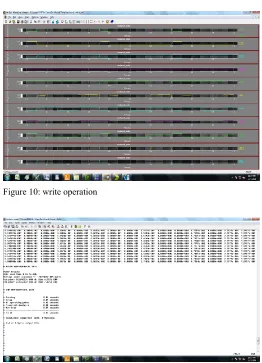
Figure 10: write operation
Figure 11: Power report
VI. CONCLUSION
An improvement of the average-8T SRAM architecture is that it does not require a write-back scheme for bit-interleaving, and it displays a competitive subject. Never the less, within the case of an typical-8T SRAM architecture established on a sophisticated technological know-how such as a 22-nm FinFET technology, full-swing LBL can't be done owing to the exchange-off between the readability and the read extend. As a consequence, the gate of the learn buffer cannot be driven by using a full VDD, resulting in a considerably large read delay in a low-voltage neighborhood. Extra, the RBLs in the unselected columns are unnecessarily discharged for the duration of the write operation, resulting within the consumption of a tremendous quantity of dynamic vigour in the write operation. In the proposed differential SRAM, the alternate-off between the read stability and the read delay is eradicated. Accordingly, it may be concluded that the proposed SRAM based on the 22-nm FinFET science displays a greatly smaller read prolong and consumes much less vigour with a somewhat smaller discipline than the usual-8T SRAM.
REFERENCES
[1]. L. Changet al., “An 8T-SRAM for variability tolerance and low-voltage operation in high-performance caches,” IEEE J. Solid-State Circuits, vol. 43, no. 4, pp. 956–963, Apr. 2008. [2]. N. Verma and A. P. Chandrakasan, “A 256 kb 65 nm 8T subthreshold SRAM employing sense-amplifier redundancy,” IEEE J. Solid-State Circuits, vol. 43, no. 1, pp. 141–149, Jan. 2008.
[3]. T.-H. Kim, J. Liu, J. Keane, and C. H. Kim, “A 0.2 V, 480 kb subthreshold SRAM with 1 k cells per bitline for ultra-low-voltage computing,” IEEE J. Solid-State Circuits, vol. 43, no. 2, pp. 518–529, Feb. 2008.
[4]. B. H. Calhoun and A. P. Chandrakasan, “A 256-kb 65-nm sub-threshold SRAM design for ultra-low-voltage operation,” IEEE J. Solid-State Circuits, vol. 42, no. 3, pp. 680–688, Mar. 2007.
Available online: https://edupediapublications.org/journals/index.php/IJR/ P a g e | 3743 [6]. J. Maiz, S. Hareland, K. Zhang, and P. Armstrong,
“Characterization of multi-bit soft error events in advanced SRAMs,” in IEDM Tech. Dig., Dec. 2003, pp. 21.4.1–21.4.4. [7]. J. Chang, J.-J. Kim, S. P. Park, and K. Roy, “A 32 kb 10T sub-threshold SRAM array with bit-interleaving and differential read scheme in 90 nm CMOS,”IEEE J. Solid-State Circuits, vol. 44, no. 2, pp. 650–658, Feb. 2009.
[8]. M. Khayatzadeh and Y. Lian, “Average-8T differential-sensing subthreshold SRAM with bit interleaving and 1k bits per bitline,” IEEE Trans. Very Large Scale Integr. (VLSI) Syst., vol. 22, no. 5, pp. 971–982, May 2014.
[9]. K. Ronse et al., “Opportunities and challenges in device scaling by the introduction of EUV lithography,” in IEDM Tech. Dig., Dec. 2012, pp. 18.5.1–18.5.4.
[10]. (Jul. 2013). BSIM-CMG 107.0.0 Multi-Gate MOSFET Compact Model. [Online].
http://wwwdevice.eecs.berkeley.edu/bsim/?page= BSIMCMG_LR