Available online: https://edupediapublications.org/journals/index.php/IJR/ P a g e | 352
Graph Based Transistor Network Generation Method for
Super Gate Design
Bandikolu Suresh1, Rajesh Kanuganti2 & N.Chandrashekhar3
1M-Tech, Dept. of ECE,Khammam Institute of Technology and Science, Khammam.
2Associate Professor, Dept. of ECE,Khammam Institute of Technology and Science, Khammam.
3Associate Professor& HOD,Dept. of ECE,Khammam Institute of Technology and Science, Khammam.
Abstract
Transistor community optimization represents an effective way of enhancing VLSI circuits. This paper proposes a singular approach to routinely generate networks with minimum transistor rely, beginning from an irredundant sum-of-products expression as the input. The technique is able to supply each collection– parallel (SP) and non-SP transfer preparations, enhancing speed, strength dissipation, and place of CMOS gates. Experimental results display predicted profits in evaluation with associated processes.
Keyword: -Bounded mode, Unbounded Mode, SP.
1. INTRODUCTION
IN VLSI digital layout, the signal put off propagation, strength dissipation, and vicinity of circuits are strongly related to the wide variety of transistors (switches). Hence, transistor association optimization is of unique hobby when designing fashionable mobile libraries and
Available online: https://edupediapublications.org/journals/index.php/IJR/ P a g e | 353
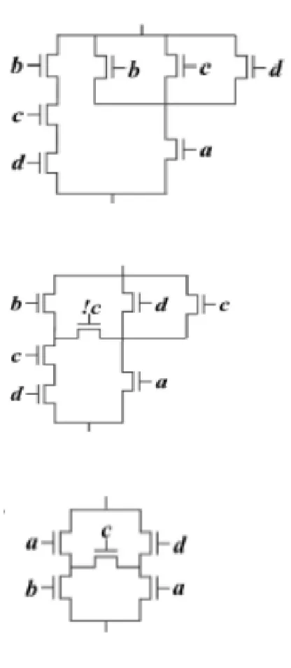
Fig. 1. Transistor networks corresponding to (1). (a) SP solution from factored form. (b) NSP from present graph-based totally era techniques. (c) Optimum NSP answer.
For instance, take into account a given characteristic represented by using the following equation:
For this capacity, factorization techniques can bring the SP organize seemed in Fig. 1(a), containing seven transistors. Existing diagram primarily based strategies, thusly, can give the NSP arrangement seemed in Fig. 1(b), additionally with seven transistors. Be that as it can, the correct recreation plan comprised of just 5 transistors, as regarded in Fig. 1(c), is not found by any of these techniques.
2.RELEGATED WORK 2.1 Problem statement
I N VLSI virtual design, the sign delay propagation, power dissipation, and region of circuits are strongly related to the wide variety of transistors (switches). [4-5]Hence, transistor arrangement optimization is of unique interest when designing fashionable cell libraries and
custom gates. Switch primarily based
Available online: https://edupediapublications.org/journals/index.php/IJR/ P a g e | 354
and optimizing transistor networks.[3] Most conventional solutions are primarily based on factoring Boolean expressions, wherein best series–parallel (SP) institutions of transistors can be received from factored paperwork. On the opposite hand, graph-based totally methods are able to locate SP and additionally non-SP (NSP) preparations with ability reduction in transistor rely. Despite the efforts of preceding works, there is still a room for improving the era of transistor networks.
2.2 Suggest method
The proposed approach comprises most important modules: 1) the kernel identity and a pair of) the switch network composition. The former gets an ISOP F and identifies character NSP and SP transfer networks, representing sub capabilities of f. [2]The latter composes those networks into a single community by way of performing common sense sharing. The furnished output is an optimized switch community
Representing the goal feature f.
3.TRANSISTOR STACK BOUNDING Switch systems can be misused by using transfer-based totally advances, which show a few confinements or policies to be trailed with the aid of originators. [1]For instance, in the traditional CMOS plan innovation, the greatest quantity of stacked transistors is commonly constrained to four. Such obstacle is executed
with a particular end aim to live faraway from execution corruption. Notice that there is a decrease bound on the stacked transistors in switch systems. This decrease certain relates to the bottom choice chain (MDC) property of the spoke to Boolean capacities [19]. In this sense, an intriguing thing to manipulate (or to restrain) the quantity of stacked transistors turned into integrated into our approach. The method can work in two execution modes, restrained and unbounded, as depicted under.
A. Bounded mode
Available online: https://edupediapublications.org/journals/index.php/IJR/ P a g e | 355
B. Unbounded Mode
When jogging inside the unbounded mode, there is no confinement of transistor stacking, i.E., the bound variable isn't always taken into consideration. Fundamentally, in reality the combination transistor tally of the device is taken as metric fee. Subsequently, there are cases that the structures created thru the unbounded mode result much less transistors whilst contrasted and limited preparations. In addition, those extraordinary modes are very useful to analyze the tradeoff between circuit territory and execution.
(a)
(b)
Two viable transistor networks generated with the aid of the proposed method to put into effect the feature described in (13), considering both execution modes. (a) Unbounded. (b) Bounded. Example 12: In order to illustrate those execution modes, recollect the following equation:
F = !a ・ !b ・d + !a ・ !c ・d + !b ・ !c ・ !d.
(13)
The network proven in Fig. 21(a) is obtained whilst jogging the technique inside the unbounded mode. Notice that, in this network,
the dimensions of the transistor stack !A ・ d ・
!B ・ d is >three, which is the wide variety of
literals of the smallest dice from (thirteen). When jogging the method in the bounded mode, it's miles viable to ensure transistor stacks with at most three gadgets, as proven in Fig. 21(b). On one hand, the bounded community gives an overhead of one transistor in assessment with the unbounded solution. On the opposite hand, the bounded answer has smallest transistor stacks. In this experience, you can bear in mind the bounded solution while concentrated on overall performance or the unbounded answer for smaller vicinity.
Available online: https://edupediapublications.org/journals/index.php/IJR/ P a g e | 356
Bounded
Unbounded
Layout
SP
Bounded
Available online: https://edupediapublications.org/journals/index.php/IJR/ P a g e | 357
Simulation Output SP
Bounded
Unbounde
5.CONCLUSION
This paper defined an efficient graph-based totally approach to generate optimized transistor (transfer) networks. Our technique generates greater wellknown arrangements than the
standard SP institutions. Experimental
consequences confirmed a significant discount within the wide variety of transistor needed to implement common sense networks, whilst as compared with those generated by current related procedures. It is known that the transistor matter minimization in CMOS gates
may additionally enhance the overall
performance, electricity dissipation, and
location of virtual ICs. In a standard factor-of-view, the proposed method produces green switch preparations pretty useful to be explored by unique IC technologies primarily based on switch principle.
6.REFERENCE
[1] Y.-T. Lai, Y.-C. Jiang, and H.-M. Chu, “BDD decomposition for mixedCMOS/PTL logic circuit synthesis,” in Proc. IEEE Int. Symp. CircuitsSyst. (ISCAS), vol. 6. May 2005, pp. 5649–5652.
Available online: https://edupediapublications.org/journals/index.php/IJR/ P a g e | 358
[3] T. J. Thorp, G. S. Yee, and C. M. Sechen, “Design and synthesis ofdynamic circuits,” IEEE Trans. Very Large Scale Integr. (VLSI) Syst.,vol. 11, no. 1, pp. 141–149, Feb. 2003. [4] A. I. Reis and O. C. Andersen, “Library sizing,” U.S. Patent 8 015 517,Jun. 5, 2009. [5] R. Roy, D. Bhattacharya, and V. Boppana, “Transistor-level optimizationof digital designs with flex cells,” Computer, vol. 38, no. 2, pp. 53–61,Feb. 2005.
[6] M. Rostami and K. Mohanram, “Dual-vth independent-gate FinFETsforlow power logic circuits,” IEEE Trans. Comput.-Aided Design Integr.Circuits Syst., vol. 30, no. 3, pp. 337– 349, Mar. 2011.
[7] M. H. Ben-Jamaa, K. Mohanram, and G. De Micheli, “An efficientgate library for ambipolar CNTFET logic,” IEEE Trans. Comput.-AidedDesignIntegr. Circuits Syst., vol. 30, no. 2, pp. 242–255, Feb. 2011.
[8] M. C. Golumbic, A. Mintz, and U. Rotics, “An improvement on thecomplexity of factoring
read-once Boolean functions,” Discrete
Appl.Math., vol. 156, no. 10, pp. 1633–1636, May 2008
Authors Profiles
BANDIKOLU SURESH
He is Pursuing M-Tech (VLSI system design) Degree from Khammam Institute of Technology and Science(JNTU HYDERABAD), Ponnekal, Khammam, in (2015-2017) 2017, and B-Tech Degree from Laqshya Institute Of Technology and Science (JNTU HYDERABAD), Thanikella , Khammam,in( 2010-2014) 2014, all in Electronics and Communication engineering.
RAJESH KANUGANTI
Available online: https://edupediapublications.org/journals/index.php/IJR/ P a g e | 359
Associate Professor in Khamma Institute of
Technology and Science(KITS),
Khammam,Telangana,India. He is having 9 years’ experience in teaching field.
N.CHANDRASHEKHAR