Available online: https://edupediapublications.org/journals/index.php/IJR/ P a g e | 112
A Research Study of Power Impact of Loop Buffer Schemes
for Biomedical Wireless Sensor Nodes
Prof.Dr.G.Manoj Someswar
1, A.Suman Kumar Reddy
21. Research Supervisor, Dr.APJ Abdul Kalam Technical University, Lucknow, U.P.,
India
2. Research Scholar, Dr.APJ Abdul Kalam Technical University, Lucknow, U.P., India
Abstract
The plan of current implanted frameworks is
obliged by the necessities of present day installed
applications. A considerable lot of these
applications require not just supported operation
for drawn out stretches of time, yet additionally
to be executed on battery controlled frameworks.
Under the imperative of not being
mains-associated, the nonappearance of wires to supply
a steady wellspring of vitality causes that the
utilization of a vitality gathering source or an
incorporated vitality provider restrains the
operation time of these electronic gadgets.
Direction memory associations are called
attention to as one of the real wellsprings of
vitality utilization in installed frameworks. As
these frameworks are portrayed by prohibitive
assets and a low-vitality spending plan, any
improvement that is presented in the direction
memory association permits to diminish the
vitality utilization, as well as to have a superior
circulation of the vitality spending plan all
through the installed framework. This Ph.D.
theory concentrates on the examination,
investigation, proposition, usage, and assessment
of low-vitality streamlining procedures that can
be utilized as a part of the guideline memory
associations of implanted frameworks. Genuine
installed uses of the specific sub-domain of
remote sensor hubs are utilized as benchmarks to
appear, examine, and authenticate the benefits
and disservices of every last one of the ideas in
which this Ph.D. proposal depends on.
The first key commitment is the efficient
investigation of existing low-vitality improvement
systems that are utilized as a part of guideline
memory associations, delineating their similar
points of interest, disadvantages, and exchange o
s. Over that, the exploratory assessment that is
introduced in this Ph.D. proposition utilizes a
precise strategy with a specific end goal to have
an exact estimation of parasitic and exchanging
movement. Because of this reality, this
assessment guides implanted frameworks
architects to settle on the right choice in the
exchange o s that exist between vitality spending
plan, required execution, and region cost of the
inserted framework. The second key
commitment is the improvement of an abnormal
state vitality estimation device that, for a given
application and compiler, permits the
investigation of building and compiler
configurations, as well as of code changes that
Available online: https://edupediapublications.org/journals/index.php/IJR/ P a g e | 113 association. The third key commitment is the
proposition and examination of a few promising
usage of vitality efficient direction memory
associations for a specific set of utilization codes
and installed designs. In view of the past
commitments, the work that is exhibited in this
Ph.D. proposition demonstrates why additionally
upgrading direction memory associations from
the vitality utilization perspective will remain a
critical pattern later on.
Keywords:
ITRS (International TechnologyRoadmap for Semiconductors), DMH (Data Memory Hierarchy), IMO (Instruction Memory Organization ), LB (Loop Buffer), CELB (Central Loop Buffer Architecture for Single Processor Organization )
INTRODUCTION
In this research paper, the circle buffer idea
is connected, all things considered, inserted
applications that are broadly utilized as a part
of the hubs of biomedical remote sensor
systems, to demonstrate which plan of circle
buffer is more reasonable for applications
with certain conduct. Post-design
re-enactments exhibit that an exchange o exists
between the unpredictability of the circle
buffer engineering and the vitality reserve
funds of using it. Hence, the utilization of
circle buffer designs keeping in mind the end
goal to streamline the guideline memory
association from the vitality efficiency
perspective ought to be assessed precisely,
considering two elements. To start with, the
level of the execution time of the application
that is identified with the execution of
circles. Second, the conveyance of the
execution time rate over every last one of the
circles that shapes the application.
As appeared in this research paper, installed
frameworks have different qualities
contrasted and universally useful
frameworks. From one perspective,
implanted frameworks consolidate
programming and equipment to run a
specific and fixed set of uses. In any case,
these applications differ enormously in their
qualities, since they run from media buyer
gadgets to industry control frameworks. On
the other hand, not at all like universally
useful frameworks, implanted frameworks
have confined assets and a low-vitality
spending plan. Notwithstanding these
limitations, implanted frameworks regularly
need to give high calculation ability, meet
continuous requirements, and fulfil changed,
tight, and time conflicting imperatives with a
specific end goal to make themselves solid
and unsurprising. Area 1.2 demonstrates that
the blend of these necessities and the way
that the outstanding issue of the memory
divider turns out to be much more
noteworthy in implanted frameworks make
the decline of the aggregate vitality
utilization of the framework turn into a major
test for architects, who need to consider the
execution of the framework, as well as its
vitality utilization. Works like illustrate that
the IMO (Instruction Memory Organization)
and the DMH (Data Memory Hierarchy )
take bits of chip range and vitality utilization
that are not insignificant. Truth be told, both
memory structures now represent about 40
Available online: https://edupediapublications.org/journals/index.php/IJR/ P a g e | 114 plan of an inserted guideline set processor
stage (see Figure 1). In this way, the
enhancement in vitality utilization of both
memory designs turns out to be critical.
J. Villarreal et al. demonstrated that 77 % of
the execution time of an application is spent
in circles of 32 guidelines or less. This
showed in utilizations of flag and picture
handling, a significant measure of the
aggregate execution time was spent in little
program portions. On the off chance that
these could be put away in littler memory
banks (e.g., as a LB (Loop Buffer), the
dynamic vitality utilization could be
decreased significantly. The vitality sparing
highlights of the circle buffer idea can be
acquired in Figure 1, where it is
demonstrated that gets to in a little memory
have bring down vitality utilization than in
an extensive memory. This is the base of the
circle buffer idea, which is a plan to diminish
the dynamic vitality utilization in the IMO.
Besides, managing an account is identified as
an effective technique to decrease the
spillage vitality utilization in recollections.
Aside from the likelihood of utilizing
low-control working modes, the utilization of
memory banks lessens the effective
capacitance as contrasted and a solitary solid
memory.
Installed frameworks constitute the
computerized space of the hubs of a WSN
(Wireless Sensor Network ). They are
generally sent in a few sorts of frameworks
running from mechanical checking to
medicinal applications. Especially, for the
biomedical space, the data that is prepared
and transmitted is confidential or requires
validation in most of the cases. Because of
this reality, it isn't strange that two
applications like a HBD (Heartbeat Detection
) calculation and a cryptographic calculation,
for example, AES (Advanced Encryption
Standard ) can be found in the hubs of
biomedical WSNs. These two genuine
installed applications are utilized as a part of
this Chapter as contextual analyses to assess
the vitality decreases accomplished by the
utilization of the IMOs that depend on the
circle buffer idea. memories designed by
tools using TSMC 90nm LP process.
Available online: https://edupediapublications.org/journals/index.php/IJR/ P a g e | 115
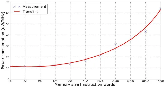
Figure 1: Power consumption per access in 16-bit word SRAM-based
In this Chapter, the loop buffer concept is
applied in the two real-life embedded
applications that are described in the previous
paragraph. The loop buffer architectures that are
analysed in this Chapter are the CELB ( Central
Loop Buffer Architecture for Single Processor
Organisation ) and the BCLB (Banked Central
Loop Buffer Architecture ). The contributions of
this Chapter include:
An analysis of real-life embedded applications
that is used to show which type of loop buffer
scheme is more suitable for applications with
certain behaviour. The use of post-layout
simulations to evaluate the energy impact of the
loop buffer architectures, in order to have an
accurate estimation of parasitic and switching
activity. Gate-level simulations demonstrate that
a trade-o exists between the complexity of the
loop buffer architecture and the power benefits
of utilising it. The use of loop buffer
architectures in order to optimise the IMO from
the energy efficiency point of view should be
evaluated carefully. Two factors have to be
taken into account in order to implement an
energy efficient IMO based on a loop buffer
architecture:
The percentage of the execution time of the
application that is related to the execution of the
loops included in the application. The
distribution of the execution time percentage,
which is related to the execution of the loops,
over each one of the loops that form the
application.
Analysts have exhibited that the IMO can add to
a substantial level of the aggregate vitality
utilization of the implanted framework. The
majority of the building upgrades that have been
utilized to diminish the vitality utilization of the
IMO have influenced utilization of the circle To
cradle idea. Works exhibit the most conventional
utilization of the circle buffer idea: the CELB
(Central Loop Buffer Architecture for Single
Processor Organization ). Work proposed a
configurable guideline store, which could be
custom-made for a specific application keeping
in mind the end goal to use the sets efficiently,
with no expansion in reserve size, associatively,
or access time. Work proposed an option way to
deal with identify and evacuate pointless
tag-checks at run-time. Utilizing execution
impressions, which were recorded already in a
BTB (Branch Target Buffer ), it was conceivable
to preclude the tag-checks for all guidelines in a
got square. On the off chance that circles could
be identified, brought, and decoded just once,
work proposed a building upgrade that could
switch o the bring and the disentangle rationale.
The guidelines of the circle were decoded and
put away locally, from where they were
executed. The vitality reserve funds originated
from the lessening in memory gets to and also
the lesser utilization of the interpret rationale.
With a specific end goal to stay away from any
execution corruption, work actualized a little
guideline buffer that depended on the definition,
the identification and the use of unique branch
directions. This design upgrade had neither an
address label store nor a substantial piece related
with each circle reserve passage. Work assessed
the Filter Cache. This upgrade was a strangely
little first-level store that sacrificed a part of
Available online: https://edupediapublications.org/journals/index.php/IJR/ P a g e | 116 was just required when a miss happens in the
Filter Cache, else it stayed in standby mode. In
view of this unique circle buffer improvement,
work displayed a building upgrade that
distinguished the chance to utilize the Filter
Cache, and empowered or impaired it
progressively. Likewise, work presented a DFC (
Decoder Filter Cache ) in the IMO to give
straightforwardly decoded guidelines to the
processor design, decreasing the utilization of
the direction bring and unravel rationale.
Moreover, work proposed a plan, where the
compiler produced code so as to lessen the
likelihood of a miss on the up and up buffer
reserve. In any case, the disadvantage of this
work was the exchange o between the execution
corruption and the power investment funds,
which was made by the choice of the
fundamental squares.
Parallelism is a notable answer for expanding
execution efficiency. Because of the way that
circles frame the most critical piece of an
application, circle change systems are connected
to misuse parallelism inside circles on
single-strung models. Concentrated assets and
worldwide et al. correspondence make these
designs less vitality efficient. With a specific end
goal to lessen these bottlenecks, a few
arrangements that utilized various circle buffers
were proposed in writing. Works are cases of the
work done in this field: the CLLB ( Clustered
Loop Buffer Architecture with Shared
Loop-Nest Organization ). From one perspective, work
introduced a dispersed control-way engineering
for ( Distributed Very Long Instruction Word )
processors, which defeated the adaptability issue
of VLIW (Very Long Instruction Word )
control-ways. The principle thought was to
circulate the get and the unravel rationale
similarly that the enlist le was dispersed in a
multi-group information way. Then again, work
proposed a multi-centre design that broadened
customary multi-centre frameworks in two ways.
In the first place, it gave a double mode scalar
operand system to empower efficient between
centre correspondence without utilizing the
memory. Second, it could compose the centres
for execution in either coupled or decoupled
mode through the compiler. These two modes
made an exchange o between correspondence
idleness and flexibility, which ought to be
enhanced relying upon the required parallelism.
Work [BSBD +08] dissected an arrangement of
circle buffer designs for efficient conveyance of
VLIW guidelines, where the assessment
incorporated the cost of the memory gets to and
the wires that were essential keeping in mind the
end goal to disseminate the direction bits. For
more subtle elements.
The CELB engineering and the CLLB design
can be actualized in view of memory banks or
without them. Power administration of managed
an account recollections has been explored from
different points including equipment, OS (
Operating System ) and compiler. Utilizing
memory get to designs in installed frameworks,
L. Benini et al. proposed a calculation to
segment on-chip SRAM (Static Random Access
Memory ) into multi-banks that could be gotten
to autonomously. X. Fan et al. exhibited memory
controller strategies for memory structures with
Available online: https://edupediapublications.org/journals/index.php/IJR/ P a g e | 117 Utilized a compiler guided way to deal with
decide the working methods of memory banks in
the wake of booking the memory operations. As
it is conceivable to see from past methodologies,
the downside of utilizing different buffers is
typically the expansion of the rationale that
controls the banks, which has the benefit of
further diminishing the spillage vitality
utilization. This reality prompts the expansion of
the interconnect capacitances, and also the
decrease of the conceivable dynamic vitality
funds that are identified with the entrance to
littler recollections. Most methodologies that are
identified with stores expect that the mechanized
tuning is done statically, implying that the tuning
is done once amid application configuration
time. A. Ghosh et al. introduced a heuristic that,
through an expository model, straightforwardly
decided the configuration of the reserve in light
of the architect's execution requirements and
application qualities. Other store tuning
methodologies could be utilized powerfully,
while the application was executed.
General-Purpose Processor
The general-purpose processor architecture is
designed using the tools from Target Compiler
Technologies. For more information. The ISA
(Instruction Set Architecture ) of this processor
architecture is composed of integer arithmetic,
bitwise logical, compare, shift, control, and
indirect addressing I/O instructions. Apart from
support for interrupts and on-chip debugging,
this processor architecture supports
zero-overhead looping control hardware, which
allows fast looping over a block of instructions.
Once the loop is set using a special instruction,
additional instructions are not needed in order to
control the loop, because the loop is executed a
pre-specified number of iterations (known at
compile time). This loop buffer implementation
supports branches, and in cases where the
compiler cannot derive the loop count, it is
possible to inform the compiler through source
code annotations that the corresponding loop
will be executed at least N times, and at most M
times, such that no initial test is needed to check
whether the loop has to be skipped. The status of
this dedicated hardware is stored in the
following set of special registers:
LS Loop Start address register. This register
stores the address of the first instruction of the
loop. LE Loop End address register. This
register stores the address of the last instruction
of the loop. LC Loop Count register. This
register stores the remaining number of
iterations of the loop.
LF Loop Flag register. This register keeps track
of the hardware loop activity. Its value
represents the number of nested loops that are
active.
The experimental framework uses an I/O
interface in order to provide the capability of
receiving and sending data in real-time. This
interface is implemented in the processor
architecture by FIFO ( First In, First Out )
architectures that are directly connected to the
register le. The data memory that is required by
this processor architecture in order to be a
general-purpose processor is a memory with a
Available online: https://edupediapublications.org/journals/index.php/IJR/ P a g e | 118 required program memory is a memory with a
Available online: https://edupediapublications.org/journals/index.php/IJR/ P a g e | 119
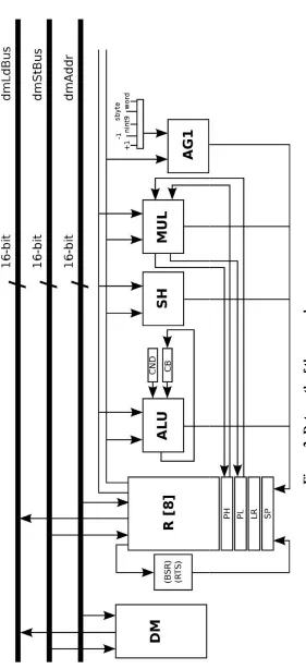
Figure
2:
D
a
ta
-pa
th o
f t
h
e ge
ne
ral
-pu
rpo
se
pro
ce
ss
Available online: https://edupediapublications.org/journals/index.php/IJR/ P a g e | 120 Figure 2 presents the information way of this
processor engineering, where the primary pieces
are DM (Data Memory ), R (Register File ),
ALU (Arithmetic Rationale Unit ), SH (Shift
Unit ), MUL (Multiplication Unit ), and AG
(Address Generation Unit ). The address age unit
species the following location as a typical
guideline word on account of the word mark, as
negative offsets to the stack pointer enlist on
account of the nint9 name, and as a relative
offset of short bounce directions on account of
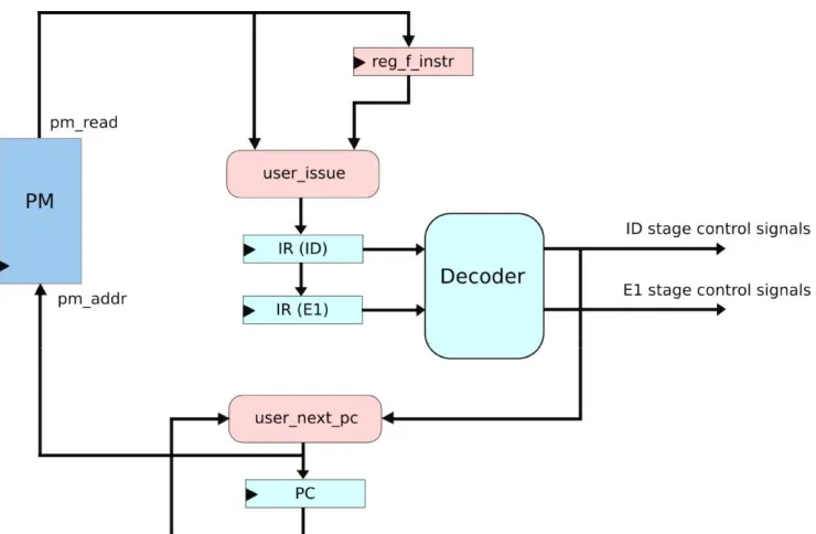
the sbyte name. In Figure 3, the primary pieces
are PM (Program Memory ), PC (Program
Counter), and the registers IR (ID) and IR (E1)
which are identified with the translate and the
execute phase of the processor pipeline.
Figure 3: Control-path of the general-purpose processor
Optimised Processor for the Heartbeat
Detection Algorithm
The processor architecture that is optimised for
the heartbeat detection algorithm is based on the
processor architecture. This Section presents the
modifications and the optimisations that are
performed in order to build this optimised
processor architecture. From the deep analysis
that has to be performed to design the ASIP
(Application-Specific Instruction-Set Processor )
design for the heartbeat detection algorithm, a
loop is pointed out as the performance
bottleneck in this specific algorithm. This loop
performs the convolution operation, which is the
core of the CWT (Continuous Wavelet
Transform ). A signed multiplication, whose
result is accumulated in a temporally variable, is
performed inside of this critical loop. The
execution of this instruction is 72 % of the
execution time of the algorithm according to
profiling information. Therefore, in order to
improve the performance, the MUL unit is
modified to multiply two signed integers and
accumulate, without shifting, the result of the
multiplication. This optimisation saves energy
Available online: https://edupediapublications.org/journals/index.php/IJR/ P a g e | 121 complexity of the MUL unit and the execution
time of the application.
The heap operations that are identified with the
past MUL operation are consolidated in a redone
guideline keeping in mind the end goal to be
executed in parallel. Be that as it may, in the
broadly useful processor, it is just conceivable to
load and store information from a similar
memory once per phase of the pipeline. To
tackle this bottleneck, the fundamental
information memory is part in two
indistinguishable information recollections: DM
(Data Memory) and CM (Constant Memory ).
With a specific end goal to get to two
recollections in parallel, another address
generator (AG2) is made to such an extent that
the heap and the store operations from the DM
and the CM can be performed at a similar phase
of the pipeline. As the information registers of
the MUL unit can be stacked straightforwardly,
another modification can be performed. The
parallel load and the MUL direction are
consolidated, by including another phase in the
pipeline and making a custom guideline that
coordinates the two directions. The MUL
direction is then executed in the second phase of
the pipeline, while the parallel load guideline is
executed in the first phase of the pipeline. After
this last modification, the MUL operation that is
incorporated into the principle basic circle of
this calculation is performed utilizing just a
single gathering guideline. In a similar way to
the MUL operation, another critical loop is
optimised by combining load, select, and equal
instructions in order to be executed in parallel.
This instruction is created adding the
functionality of the equal and the select
instructions, and combining both of them with a
normal load operation. The functional unit ALU
2 is created for this specific operation.
It should be noted that, apart from the
specialised instructions that are described in
previous paragraphs, custom techniques like
source code transformations (e.g., function
combination, loop unrolling) and mapping
optimisations (e.g., look-up tables, elimination
of divisions and multiplications, instruction set
extensions) are applied to generate a more
efficient code. All the optimisations and the
modifications that are described in this Section
result in the new processor architecture shown in
Available online: https://edupediapublications.org/journals/index.php/IJR/ P a g e | 122
F
igure
4:
D
at
a
-path
of
t
he
proces
sor
t
hat i
s opt
im
ise
d
for t
he he
art
beat
det
ect
ion
al
gori
Available online: https://edupediapublications.org/journals/index.php/IJR/ P a g e | 123 Basically, an Essentially, an address generator
(AG2) and a moment (ALU 2) are included,
notwithstanding a few pipes and ports. Aside
from that, the program counter is modified to
deal with guidelines that utilization 32-bit quick
esteems. Keeping in mind the end goal to deal
with ECG (Electrocardiogram) signals inspected
at 1KHz, the recollections that are required by
this processor design are a DM with a limit of
8K words/32 bits, and a CM with a limit of 8K
words/32 bits. Furthermore, the program
memory that is required by this processor
engineering is a memory with a limit of 1K
words/20 bits. This upgraded processor design is
a usage that depends on the work displayed in
Reference [YKH +09].
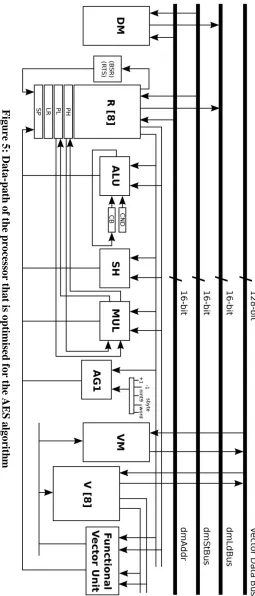
Optimised
Processor
for
the
AES
Algorithm
The processor design that is improved for the
AES calculation (see Section C.3) is construct
additionally in light of the processor engineering
that is exhibited. Dissecting this calculation, the
basic capacities are identified and upgraded so
as to enhance execution regarding clock cycles
and memory gets to. Custom procedures like
source code changes (e.g., work blend, circle
unrolling) and mapping improvements ( e.g.,
look-into tables, end of divisions and
augmentations, guideline set expansions) are
connected to produce a more efficient code.
In the outline of this streamlined processor, the
structure of the broadly useful processor is kept
in place (16-bit information way), and an
additional 128-piece information way is
included. This last information way is associated
with a VM ( Vector Memory ), a V (Vector
Register File ), and a Vector Unit (Functional
Vector Unit). This unit incorporates the AES
quickening operations, and in addition the
rationale and the number juggling directions that
this calculation requires. In this processor, the
ISA is additionally stretched out with one AES
quickening direction that has two sources of
info: a 128-piece input, which can be the state or
a round key, and a whole number information,
which shows the conduct of the guideline itself.
Contingent upon the info, the yield contains the
state or a round key. One of the upsides of this
plan is the capacity to utilize the bigger vector
units just when they are required. Every one of
the advancements and the modifications that are
introduced in this Section result in the new
processor engineering appeared in Figure 5.
Essentially, an additional 128-piece information
way is included. This additional information
way incorporates a VM ( Vector Memory ), a V
(Vector Register File ), and a Vector Unit
(Functional Vector Unit). To deal with an
information flag of bytes, the DM required by
this processor design is a memory with a limit of
1K words/16 bits, and the VM is a memory with
a limit of 64 words/128 bits. Additionally, the
required program memory is a memory with a
limit of 1K words/16 bits. This improved
processor engineering is a usage that depends on
Available online: https://edupediapublications.org/journals/index.php/IJR/ P a g e | 124
F
igure
5
: D
a
ta
-pa
th o
f t
h
e proc
es
so
r t
ha
t i
s opt
im
is
ed f
or
the A
E
S a
lgor
it
h
Available online: https://edupediapublications.org/journals/index.php/IJR/ P a g e | 125
Experimental Platform
The test stage is naturally produced for any of
the processor structures portrayed. The trial
stage is made out of a DMH, an IMO, an I/O
interface, and a processor design that is utilized
as centre of the implanted direction set processor
stage. From one perspective, the program
memory and the information memory are
SRAM-based recollections outlined by
apparatuses. Then again, the I/O interface that
gives the capacity to get and send information
progressively is associated with the I/O interface
that is portrayed.
The interface between a processor design and an
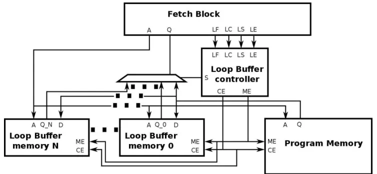
IMO is delineated in Figure 6. The
interconnections of the processor engineering,
the program memory, the circle buffer memory
and the circle buffer controller are incorporated
into this Figure. Each part that structures the
IMO is clarified in the following passages. In
our test stage, the circle buffer engineering,
which is made out of the circle buffer memory
and the circle buffer controller, can be
configured to be utilized as a CELB design or a
BCLB engineering. For straightforwardness, the
CELB engineering is utilized as a part of the
following passages to clarify the operation of the
circle buffer idea.
Available online: https://edupediapublications.org/journals/index.php/IJR/ P a g e | 126 Basically, the operation of the circle buffer idea
is as per the following. Amid the first emphasis
of the circle, the directions are gotten from the
program memory to both the circle buffer
engineering and the processor design. In this
emphasis, the circle buffer engineering records
the guidelines of the circle. Once the circle is put
away, for whatever is left of cycles, the
directions are brought from the circle buffer
design rather than the program memory. In the
last emphasis, the association between the
processor design and the program memory is
re-established, to such an extent that ensuing
directions are gotten from the program memory.
Amid the execution of non-circle parts of the
application code, guidelines are brought
straightforwardly from the program memory.
Figure 7: State-machine diagram of the loop buffer controller
The circle buffer controller screens the operation
of the circle buffer design in light of a
state-machine. This state-machine is appeared in
Figure 5.7. The six conditions of the
state-machine are:
s0 Initial state.
s1 Transition state amongst s0 and s2.
s2 State where the circle buffer design is
recording the directions that the program
memory supplies to the processor engineering.
s3 Transition state amongst s2 and s4.
s4 State where the circle buffer engineering is
giving the directions to the processor design.
s5 Transition state amongst s4 and s0.
The progress states s1, s3, and s5 are
fundamental keeping in mind the end goal to
give the control of the guideline supply from the
program memory to the circle buffer design and
the other way around. The progress amongst s4
and s1 is vital on the grounds that the body size
of a circle can change continuously ( i.e., in a
Available online: https://edupediapublications.org/journals/index.php/IJR/ P a g e | 127 calls). With a specific end goal to check
continuously whether the circle body measure
changes or not, a 1-bit tag is utilized. This tag is
related with each address that is put away on top
of it buffer memory. The circle buffer controller
checks this tag to know whether the address is
now put away on top of it buffer design or not.
Figure 8 shows how the BCLB engineering is
made out of different circle buffer recollections.
In a BCLB engineering, each memory is
associated with the processor design and the
program memory through multiplexers. The
circle buffer controller, in light of the circle
body size of the circle that is on execution,
chooses which of the accessible circle buffer
recollections is associated straightforwardly with
the program memory and the processor design.
The rationale circuit that chooses if the circle
buffer engineering is actuated is the same as the
one that is utilized as a part of the CELB design.
Keeping in mind the end goal to settle on every
one of the choices that are depicted beforehand,
the many-sided quality of the state-machine is
augmented. Nonetheless, Figure 8 demonstrates
that this modification permits the outline of the
circle buffer design to be versatile.
Figure 8: IMO interface for a BCLB architecture
This Section demonstrates the consequences of
the trial assessment of the CELB engineering
and the BCLB design. Initially, depicts the
technique that is utilized as a part of the vitality
recreations. Besides, examinations the
exploratory applications that are portrayed in
profiling data. At long last, shows and talks
about the consequences of the vitality
re-enactments.
Simulation Methodology
The reproduction technique that is utilized as a
part of the exploratory assessment is depicted by
the accompanying advances: Application
mapping. The chose application is mapped to the
framework design that it will be mimicked. The
I/O information associations of the framework
are utilized by the installed frameworks creator
to authenticate the right usefulness of the
Available online: https://edupediapublications.org/journals/index.php/IJR/ P a g e | 128 Conduct reproduction: The mapped
application is re-enacted on the framework
design with a specific end goal to check its right
usefulness. For that reason, the ISS (Instruction
Set-Simulator ) from the Target Compiler
Technologies devices is utilized.
RTL usage: The RTL (Register-Transfer Level)
dialect depiction les of the processor engineering
are naturally created utilizing the HDL age
device from the Target Compiler Technologies
devices. The plan of the interfaces between the
DMH and the IMO must be included request to
have an entire portrayal of the entire framework
in RTL dialect. RTL union. Once every segment
of the framework has its own particular RTL
dialect portrayal le, the plan is blended. In our
RTL blend, a TSMC 90nm LP library is utilized
for a framework recurrence of 100MHz. Amid
blend, clock gating is utilized at whatever point
conceivable. Place and course. After the blend,
place and course is performed utilizing
Encounter.
Recording Activity: It is important to produce a
VCD ( Value Change Dump) le for the coveted
time interim of the net list recreation. On the off
chance that the chose time interim is the
execution time of the application, the VCD le
will contain the data of the action of each net
and each part of the entire framework when an
information outline is handled. Extraction of
energy utilization. As a final step, the data of the
normal power utilization is separated with the
assistance of Primetime.
Figure 9 shows the inputs and outcomes of each step described above
Available online: https://edupediapublications.org/journals/index.php/IJR/ P a g e | 129
.
Figure 9: Simulation methodology
Analysis of the Experimental
Applications
The aggregate vitality utilization of the
frameworks that are introduced in this Chapter is
unequivocally influenced by the utilization of
the IMO. Following the means that are depicted,
Figure 10, Figure 11, Figure 12, and Figure 13
present the primary result from the exploratory
assessment. Figure 10 and Figure 11
demonstrate the power breakdowns that are
identified with the pulse identification
calculation, while Figure 12 and Figure 13
demonstrate the power breakdowns that are
identified with the AES calculation. In these
Figures, the parts of the processor centre are
gathered. Aside from perceiving how the power
circulation changes from a plan in light of a
broadly useful processor to an ASIP outline,
these Figures show that the aggregate vitality
utilization of these frameworks is emphatically
influenced by the utilization of the IMO.
Circles command the aggregate vitality
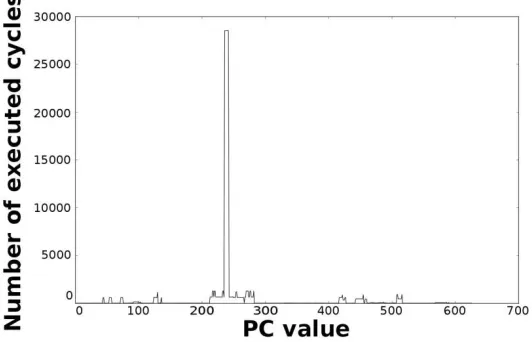
utilization of the IMO. Figure 14, Figure 15,
Figure 16, and Figure 17 show profiling data in
light of the gets to that are done in the program
address space. Figure 14 and Figure 15
demonstrate the profiles in light of the quantity
of cycles per program counter that are identified
with the pulse discovery calculation, while
Figure 16 and Figure 17 demonstrate the profiles
in view of the quantity of cycles per program
counter that are identified with the AES
calculation. It is conceivable to see from these
Figures that there are areas that are more
habitually got to than others. This circumstance
suggests the presence of circles. Aside from this
reality, it is conceivable to see from these
Figures that the application execution time of the
chose applications is ruled by just a couple of
circles.
With a specific end goal to execute vitality
efficient IMOs in view of circle buffer
structures, more detail data identified with
circles is required. Table 1, Table 2, Table 3, and
Table 4 give this data. Table 1 and Table 2
present the circle profiling data of the
frameworks that are identified with the pulse
recognition calculation, while Table 3 and Table
4 present the circle profiling data of the
frameworks that are identified with the AES
calculation. In these Tables, circles are
numbered in a similar request that they show up
in the get together code of the calculation. A
settled circle makes another level of numbering.
Accordingly, a circle named 2 relates to the
second circle experienced, while a circle named
2.1 compares to the first sub-circle experienced
on the up and up named 2. These Tables certify
the way that the execution time of the circles
commands the aggregate execution time of the
application. For example, the execution time of
the circles speaks to around 79 % of the
aggregate execution time of the pulse
Available online: https://edupediapublications.org/journals/index.php/IJR/ P a g e | 130 useful processor, and 81 % in the processor
engineering that is upgraded for this calculation.
Interestingly, in the AES calculation, the
execution time of the circles speaks to 77 % of
the aggregate execution time on account of the
universally useful processor, and 90 % in the
processor design that is enhanced for this
calculation. It is important to comment that
differences exist between calculations of a
similar application because of the source code
changes and the mapping enhancements that are
connected in the streamlined calculations
keeping in mind the end goal to create efficient
codes.
The configurations of the CELB engineering and
the BCLB design that are dissected in this
Chapter depend on the circle profiling exhibited
in Table 1, Table 2, Table 3, and Table 4. From
one perspective, the choice of the CELB
configurations depends on the little size of the
circles that have greater level of execution time.
With this system, it is expected that these
configurations are the most vitality efficient.
This presumption depends on the way that these
configurations give the most noteworthy vitality
investment funds among all the conceivable
configurations.
Figure 10: Power breakdown in the general-purpose processor running the heartbeat detection
Available online: https://edupediapublications.org/journals/index.php/IJR/ P a g e | 131
Figure 11: Power breakdown in the optimised processor running the heartbeat
Available online: https://edupediapublications.org/journals/index.php/IJR/ P a g e | 132
Figure 12: Power breakdown in the general-purpose processor running the AES
algorithm
Available online: https://edupediapublications.org/journals/index.php/IJR/ P a g e | 133
Figure 14: Number of cycles per PC in the general-purpose processor running the heartbeat
detection algorithm
Figure 15: Number of cycles per PC in the optimised processor running the heartbeat detection
Available online: https://edupediapublications.org/journals/index.php/IJR/ P a g e | 134
Figure 16: Number of cycles per PC in the general-purpose processor running the AES
Available online: https://edupediapublications.org/journals/index.php/IJR/ P a g e | 135
Figure 17: Number of cycles per PC in the optimised processor running the AES algorithm
These real vitality reserve funds help to diminish
the punishment identified with the presentation
of the circle buffer engineering in the
framework. Then again, the determination of the
BCLB configurations depends on the procedure
of taking the greatest circle body size of the
application, and cleave it by the granularity of
the littler circle body measure that the
applications contains. This procedure is utilized
as a part of these models, in light of the fact that
the correct vitality utilization of the additional
rationale that must be included the circle buffer
controller is obscure. Table 5 presents the
underlying configurations that are assessed.
With a specific end goal to finish up the
investigation of the exploratory applications, it is
important to comment that because of time
prerequisites, a framework recurrence of
100MHz is fixed. From one viewpoint, the pulse
identification calculation running on the
universally useful processor burns through 462
cycles to process an information test contained
in the information outline. Be that as it may, if
this calculation is running on the processor
advanced for this calculation, the quantity of
cycles to process a similar info test is 11 cycles.
Then again, the AES calculation running on the
universally useful processor burns through 484
cycles to process an information test contained
in the information outline. All things considered,
if this calculation is running on the processor
advanced for this calculation, the quantity of
cycles to process a similar information test is
Available online: https://edupediapublications.org/journals/index.php/IJR/ P a g e | 136
Table 1: Loop profiling of the heartbeat detection algorithm on the general-purpose processor
Start End Loop body Number of Execution
address Address size iterations time [ %]
Loop 1 33 34 2 4 0
Loop 2 44 45 2 594 0
Loop 3 54 57 4 594 1
Loop 4 72 75 4 594 1
Loop 5 92 103 12 132 1
Loop 6 124 136 13 594 3
Loop 7 160 160 1 15 0
Loop 8 236 242 7 32; 625 71
Loop 9 417 427 11 594 2
Loop 10 569 590 22 64 0
Table 2: Loop profiling of the heartbeat detection algorithm on the optimised processor
Start End Loop body Number of Execution
address address size iterations time [ %]
Loop 1 192 244 53 1; 380 70
Loop 1.1 200 205 6 1 0
Loop 2 266 271 6 350 2
Loop 3 209 302 13 768 9
Table 3: Loop profiling of the AES algorithm on the general-purpose processor
Start End Loop body Number of Execution
address address size iterations time [ %]
Loop 1 307 309 3 8 0
Loop 2 324 327 4 2 0
Loop 3 340 342 3 16 0
Loop 4 360 362 3 1; 460 3
Loop 5 383 387 5 1; 600 7
Loop 6 409 411 3 4 0
Loop 7 419 421 3 8 0
Loop 8 426 428 3 16 0
Loop 9 436 458 23 92 2
Loop 10 472 474 3 1; 392 3
Loop 11 489 491 3 1; 392 3
Loop 12 506 510 5 1; 460 6
Loop 13 519 523 5 4 0
Loop 14 926 930 5 6; 016 25
Loop 15 942 1; 000 59 40 2
Loop 16 1; 019 1; 034 16 1; 692 26
Available online: https://edupediapublications.org/journals/index.php/IJR/ P a g e | 137
Start End Loop body Number of Execution
address address size iterations time [ %]
Loop 1 519 524 6 36 5
Loop 2 544 560 17 2 1
Loop 2.1 550 555 6 0 0
Loop 3 806 837 32 91 84
Table 5: Configurations of the experimental framework
Baseline architecture CELB BCLB
HBD algorithm No loop buer 8 words 8 banks of
General-purpose processor architecture 8 words
HBD algorithm No loop buer 64 words 8 banks of
Optimised processor architecture 8 words
AES algorithm No loop buer 8 words 4 banks of
General-purpose processor architecture 8 words
AES algorithm No loop buer 32 words 4 banks of
Optimised processor architecture 8 words
Power Analysis
Table 6, Table 7, and Table 8 present the power
comes about for every framework that is
assessed. These tables demonstrate the dynamic
power, the spillage control, and the aggregate
power for all the configurations that are
introduced in Table 5. As can be seen, the power
utilization of the IMO is the whole of the power
that is devoured by the segments that the IMO
contains ( i.e., the circle buffer controller, the
circle buffer memory, and the program
memory).
Table 6: Power consumption [W] of the baseline architecture
Component Dynamic power Leakage power Total power HBD algorithm IMO 4:44 10
06
0:91 10
09
4:44 10
06
- LB Controller 0 0 0
General-purpose LB Memory 0 0 0
processor PM 4:44 10
06
0:91 10
09
4:44 10
06
HBD algorithm IMO 3:57 10
07
8:46 10
11
3:57 10
07
- LB Controller 0 0 0
Optimised LB Memory 0 0 0
processor PM 3:57 10
07
8:46 10
11
3:57 10
07
AES algorithm IMO 1:81 10
06
4:32 10
10
1:82 10
06
- LB Controller 0 0 0
General-purpose LB Memory 0 0 0
processor PM 1:81 10
06
4:32 10
10
1:82 10
06
AES algorithm IMO 1:20 10
06
2:11 10
10
1:20 10
06
- LB Controller 0 0 0
Optimised LB Memory 0 0 0
processor PM 1:20 10
06
2:11 10
10
1:20 10
06
Available online: https://edupediapublications.org/journals/index.php/IJR/ P a g e | 138
Table 7: Power consumption [W] of the IMO based on an CELB architecture
Component Dynamic power Leakage power Total power HBD algorithm IMO 1:74 10
06
1:14 10
09
1:74 10
06
- LB Controller 2:55 10
07
1:60 10
10
2:55 10
07
General-purpose LB Memory 6:97 10
08
6:60 10
11
6:97 10
08
processor PM 1:41 10
06
9:16 10
10
1:41 10
06
HBD algorithm IMO 1:40 10
07
1:77 10
10
1:40 10
07
- LB Controller 3:71 10
08
2:66 10
11
3:71 10
08
Optimised LB Memory 5:76 10
08
6:56 10
11
5:76 10
08
processor PM 4:50 10
08
8:46 10
11
4:51 10
08
AES algorithm IMO 1:76 10
06
5:25 10
10
1:76 10
06
- LB Controller 1:03 10
07
7:39 10
11
1:03 10
07
General-purpose LB Memory 9:54 10
09
2:68 10
11
9:54 10
09
processor PM 1:65 10
06
4:25 10
10
1:65 10
06
AES algorithm IMO 8:32 10
07
4:12 10
10
8:36 10
07
- LB Controller 2:43 10
07
7:53 10
11
2:47 10
07
Optimised LB Memory 1:79 10
07
1:29 10
10
1:79 10
07
processor PM 4:10 10
07
2:13 10
10
4:10 10
07
Table 8: Power consumption [W] of the IMO based on a BCLB architecture
Component Dynamic power Leakage power Total power HBD algorithm IMO 1:97 10
06
1:47 10
09
1:97 10
06
- LB Controller 4:72 10
07
3:95 10
10
4:72 10
07
General-purpose LB Memory 8:73 10
08
1:59 10
10
8:73 10
08
processor PM 1:41 10
06
9:16 10
10
1:41 10
06
HBD algorithm IMO 1:64 10
07
3:83 10
10
1:65 10
07
- LB Controller 5:51 10
08
1:40 10
10
5:51 10
08
Optimised LB Memory 6:39 10
08
1:58 10
10
6:39 10
08
processor PM 4:50 10
08
8:46 10
11
4:51 10
08
AES algorithm IMO 1:90 10
06
7:40 10
10
1:90 10
06
- LB Controller 2:35 10
07
2:72 10
10
2:35 10
07
General-purpose LB Memory 1:46 10
08
4:29 10
11
1:46 10
08
processor PM 1:65 10
06
4:25 10
10
1:65 10
06
AES algorithm IMO 6:60 10
07
4:30 10
10
6:60 10
07
- LB Controller 5:20 10
08
1:10 10
11
5:20 10
08
Optimised LB Memory 1:98 10
07
2:06 10
10
1:98 10
07
processor PM 4:10 10
07
2:13 10
10
4:10 10
07
It is conceivable to see from these Tables that
the frameworks that are advanced for the trial
applications dependably devour less power than
the broadly useful frameworks. Accordingly, the
presentation of the CELB engineering and the
BCLB design does not affect this vitality
utilization slant. Breaking down Table 7, it is
Available online: https://edupediapublications.org/journals/index.php/IJR/ P a g e | 139 the dynamic energy of these frameworks in
connection to the gauge designs. This is on
account of most of the directions are gotten from
a little memory rather than the expansive
memory that structures the program memory.
Then again, the CELB structures have an
expansion in the spillage control utilization in
connection to the standard designs, because of
the presentation of the circle buffer engineering.
It is likewise conceivable to see the significance
of the circle buffer controller in the IMO, which
accounts from the 5 % of the power utilization
of the IMO in the framework where the AES
calculation is running on the universally useful
processor, to 30 % in the framework where the
AES calculation is running on the processor
design improved for this calculation.
Utilizing the profiling data exhibited in Table 1,
Table 2, Table 3, and Table 4, and the power
comes about acquired from the re-enactments of
the frameworks displayed in Table 5, it is
conceivable to assess whether the underlying
configurations for the CELB design are chosen
effectively from the vitality utilization
perspective.
For the pulse recognition calculation running on
the broadly useful processor, Figure 18
demonstrates the power decreases that can be
accomplished for all the conceivable
configurations. In the configuration of 8 words,
the 73 % of the execution time of the application
is on circles, while in whatever remains of the
configurations this rate is 79 %. It is conceivable
to see that in this situation, the best
configuration is a circle buffer memory of 16
words, on the grounds that the expansion of the
utilization of the circle buffer memory repays
the punishment presented by utilizing a greater
circle buffer engineering.
Figure 19 demonstrates the power decreases that
can be accomplished for all the conceivable
configurations when the pulse location
calculation is running on the processor
engineering advanced for this calculation. In the
configuration of 8 words, the 2 % of the
execution time of the application is on circles;
this rate is 11 % in the configuration of 16 and
32 words; while in the configuration of 64 words
this rate is 81 %. It is conceivable to see that in
this situation, the main configuration that brings
vitality investment funds is the circle buffer
memory of 64 words. The rates of the execution
time of whatever remains of configurations don't
remunerate the punishment presented by
utilizing a circle buffer design.
For the AES calculation running on the broadly
useful processor, Figure 20 demonstrates the
power diminishments that can be accomplished
for all the conceivable configurations. In the
configuration of 8 words, the 47 % of the
execution time of this application is on circles;
in the configuration of 16 words this rate is 70
%; in the configuration of 32 words this rate is
75 %; while in the configuration of 64 words
this rate is 77 %. It is conceivable to see that in
this situation, the best configuration is a circle
buffer memory of 32 words, in light of the fact
that the expansion of the utilization of the circle
buffer engineering repays the punishment
presented by utilizing a greater circle buffer
memory. In addition, the little increment in the
Available online: https://edupediapublications.org/journals/index.php/IJR/ P a g e | 140 32 words to 64 words does not remunerate the
expansion in the spillage control utilization that
this last circle buffer engineering has.
Figure 21 demonstrates the power decreases that
can be accomplished for all the conceivable
configurations when the AES calculation is
running on the processor engineering advanced
for this calculation. In the configuration of 8
words, the 5 % of the execution time of the
application is on circles; in the configuration of
16 words this rate is 6 %; while in the
configuration of 32 and 64 words this rate is 90
%. It is conceivable to see that in this situation,
the best configuration is a circle buffer memory
of 32 words. The rates of the execution time of
the application for the 8 and the 16 words
configurations don't remunerate the punishment
presented by utilizing a circle buffer design.
Additionally in this situation, the little increment
in the level of the execution time of the
application from the configuration of 32 words
to 64 words does not remunerate the expansion
in the spillage control utilization that this last
circle buffer engineering has.
Figure 18: HBD algorithm running on the general-purpose processor using different
Available online: https://edupediapublications.org/journals/index.php/IJR/ P a g e | 141
Figure 19: HBD algorithm running on the optimised processor using different configurations
for the CELB architecture
Figure 20: AES algorithm running on the general-purpose processor using different
Available online: https://edupediapublications.org/journals/index.php/IJR/ P a g e | 142
Figure 21: AES algorithm running on the optimised processor using different
configurations for the CELB architecture
Examining Table 8, it is conceivable to see that
additionally in these structures, there is a
lessening in the dynamic power utilization of
these frameworks in connection to the standard
designs. In any case, it is conceivable to see that
these designs now and again don't offer as great
vitality investment funds as the CELB structures
offer, in light of the fact that the framework
suffers an expansion in both the dynamic and the
spillage control utilization with the presentation
of these circle buffer models. Initially, in the
dynamic power utilization, the circle buffer
controller of the BCLB engineering has higher
multifaceted nature than in the CELB design.
Furthermore, in the spillage control utilization,
aside from the higher multifaceted nature of the
circle buffer controller, there is more circle
buffer recollections. In these circle buffer
designs, the significance of the circle buffer
controller is expanded in the IMO, which now
represents 10 % of the power utilization of the
IMO in the AES calculation when it is running
on the broadly useful processor, and for 32 % in
the pulse location calculation running on the
processor advanced for this calculation. Utilizing
an indistinguishable data and system from in the
examination of the CELB structures, it is
conceivable to investigate whether the chose
configurations for the BCLB models are vitality
efficient.
For the pulse location calculation running on the
universally useful processor design, it is
important to dissect just the circle buffer
configurations that have 8 words, since every
one of the circles would t be able to in a circle
buffer memory of 16 words (see Table 1), and
each configuration in a BCLB engineering with
a circle buffer memory of 16 words is more
terrible as far as power utilization than a CELB
design with a circle buffer memory of 16 words.
Figure 22 demonstrates the conceivable
configurations of two circle buffer recollections,
where one of them has a fixed size of 8 words.
From this Figure, it is conceivable to see that
the best configuration is two circle buffer
recollections of 8 words each. In the event that
the vitality funds from the BCLB design and the
CELB engineering are thought about, it is
conceivable to see that for this specific situation,
it is smarter to have the CELB design. For the
pulse location calculation running on the
processor engineering streamlined for this
calculation, it is important to dissect just the
circle buffer configurations that have 64 words,
on the grounds that any configuration without a
circle buffer memory of this size won't bring
Available online: https://edupediapublications.org/journals/index.php/IJR/ P a g e | 143 Figure 23 demonstrates the configuration of two
circle buffer recollections, where one of them
has a fixed size of 64 words. From this Figure, it
is conceivable to see that the best configuration
is a circle buffer memory of 16 words together
with the circle buffer memory of 64 words. On
the off chance that the vitality investment funds
from the BCLB engineering and the CELB
design are thought about, it is conceivable to see
that for this specific situation it is additionally
Available online: https://edupediapublications.org/journals/index.php/IJR/ P a g e | 144
Figure 22: HBD algorithm running on the general-purpose processor using different
configurations for the BCLB architecture
Figure 23: HBD algorithm running on the optimised processor using different configurations
Available online: https://edupediapublications.org/journals/index.php/IJR/ P a g e | 145
Figure 24: AES algorithm running on the general-purpose processor using different
configurations for the BCLB architecture
For the AES calculation running on the
universally useful processor design, it is
important to break down all the conceivable
configurations, in light of the fact that the
execution time of the application is spread (see
Table 3). The configuration with two circle
buffer recollections of 64 words each isn't
examined, in light of the fact that this
configuration is more terrible in vitality
efficiency than the CELB engineering of 64
words, because of the expansion in vitality
utilization of the circle buffer controller. From
Figure 24, it is conceivable to see that the best
configuration is a circle buffer of 8 words
together with a circle buffer of 32 words. For
this situation, if the vitality funds from the
BCLB design and the CELB engineering are
analyzed, it is conceivable to see that for this
specific situation it is additionally better to have
the CELB engineering.
For the AES calculation running on the
processor design that is improved for this
calculation, it is important to break down just the
circle buffer configurations that have 32 words,
since every one of the circles would t be able to
in a circle buffer memory of 32 words (see Table
4). Notwithstanding, from Figure 21, it is
conceivable to see that lone circle buffer
recollections of 32 and 64 words bring vitality
investment funds. In this manner, the break
down will be centred just around the circle