Suppression of IMD3 in CMOS Power Amplifier Using Bias Circuit
of Common-Gate Transistor with Cascode Structure
Jinwon Kim, Changhyun Lee, Jinho Yoo, and Changkun Park*
Abstract—In this study, we propose a technique to improve the linearity of complementary metal-oxide semiconductor (CMOS) power amplifiers with a cascode structure. From the investigation of the influence of the impedance of an envelope signal on the linearity, we find that the load impedance of the envelope signal of the common-source transistor should be reduced. To obtain alow load impedance of the envelope signal, we reduce the value of the gate resistor of the common-gate transistor. After investigating the influences of the value of the resistance on the third-order intermodulation distortion (IMD3), we extract the optimum value of the resistance. We also consider the electrostatic discharge protection issue and the effects of the variations in the parasitic components of bond-wires, in the process of the extraction of the optimum value. To verify the feasibility of the optimization technique of the resistance of the bias circuit of the common-gate transistor of the amplifier, we design a power amplifier using a 180-nm RFCMOS process for wireless local area network (WLAN) 802.11n applications. We obtain the measured maximum linear output power of 22.2 dBm with a 26.7% power-added efficiency and a 3.72% error vector magnitude. We use an 802.11n modulated signal with 64-QAM (MCS7) at 65 Mb/s. From the measured results, we successfully verify the feasibility of the proposed optimization technique of the resistance of the bias circuit of the common-gate transistor.
1. INTRODUCTION
As the data rates of rapid wireless communication systems have increased significantly, the linearity of power amplifiers has gained significant importance [1–4]. Accordingly, many parameters define the linearity of power amplifiers, such as the third-order intermodulation distortion (IMD3), amplitude-to-amplitude (AM-AM) distortion, amplitude-to-amplitude-to-phase (AM-PM) distortion, and so on. In particular, the IMD3 directly affects the adjacent channel leakage ratio (ACLR) and adjacent channel power ratio (ACPR), which are strictly specified by wireless communication standards. As a result, various techniques to suppress the IMD3 have been researched, such as the anti-phase technique [5, 6]. This technique utilizes the cancellation of IMD3s generated by the driver and power stages of the power amplifier. The technique could therefore, be applied to multi-stage amplifiers. Another linearization technique using IMD cancellation is the feedforward technique. Although the feedforward technique can successfully suppress the IMD3, the complexity of the overall system could increase.
However, a second-harmonic termination technique directly suppresses the IMD3 [7, 8]. Fig. 1 explains why the second harmonic should be terminated and hence, suppressed. As exhibited in Fig. 1, the second harmonic generates the IMD3 through the re-modulation process. Additionally, the envelope impedance, which is presented as a second-order IM term in Fig. 2, contributes to the IMD3 asymmetry with the help of the second-harmonic impedance. As a result, the termination of the second harmonic suppresses the sideband asymmetry and the magnitude of the IMD3. This approach could be realized using the inductance induced by bond-wires [8].
Received 11 April 2019, Accepted 1 June 2019, Scheduled 13 June 2019 * Corresponding author: Changkun Park ([email protected]).
Figure 1. Spectral representation of the output signal of a nonlinear amplifier under two-tone excitation.
Figure 2. Vector representation for composition of the IMD3.
In this work, in addition to applying the second-harmonic termination technique to a CMOS power amplifier, we investigate the impedance of the envelope signal,ω2−ω1 to suppress the second-order IM directly, thereby suppressing the sideband asymmetry and magnitude of the IMD3.
2. PROPOSED ENVELOPE SIGNAL TERMINATION
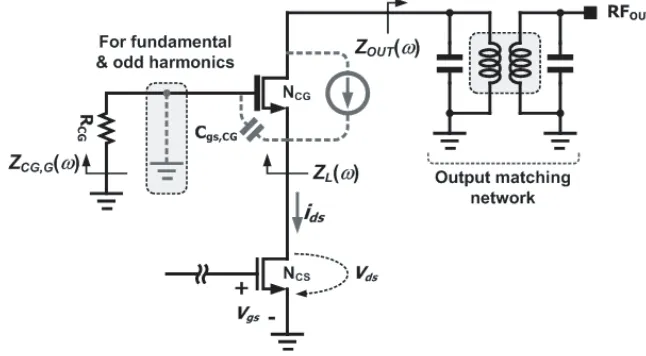
We investigate the suppression of the IMD3 by controlling the impedance of the envelope signal for the amplifier with a differential cascode structure. Fig. 3 shows the half-circuit of the differential amplifier with a cascode structure assembled in order to analyze the proposed technique of the envelope signal
termination. Because of the differential structure, the gate node of NCG becomes the AC ground for the fundamental and odd harmonic components. However, the node does not act as the AC ground for the even harmonic components [8]. For the analysis of the envelope signal termination, we inspect the power series expression of the drain current of NCS, denoted as ids in Fig. 3, as follows:
ids =gm1vgs+gm2v2gs+gm3v3gs+gd1vds+gd2v2ds+gmdvgsvds+· · · (1) where the coefficients gm, gd, and gmd are the transconductance, drain conductance, and cross conductance of NCS, respectively. With a two-tone input signal vgs = Acos(ω1t) +Acos(ω2t), the lower and upper IMD3s of the drain voltage of NCS,vds are expressed as below:
vds(2ω1−ω2) = A3ZL(ω0)×
⎧ ⎪ ⎪ ⎪ ⎪ ⎪ ⎨ ⎪ ⎪ ⎪ ⎪ ⎪ ⎩ 1
2gm2gmdZL(ω2−ω1) cos [(2ω1−ω2)t−φω2−ω1] +1
4gm2gmdZL(ω0) cos [(2ω1−ω2)t+φ2ω0] +3
4gm3cos [(2ω1−ω2)t]
⎫ ⎪ ⎪ ⎪ ⎪ ⎪ ⎬ ⎪ ⎪ ⎪ ⎪ ⎪ ⎭ (2)
vds(2ω2−ω1) = A3ZL(ω0)×
⎧ ⎪ ⎪ ⎪ ⎪ ⎪ ⎨ ⎪ ⎪ ⎪ ⎪ ⎪ ⎩ 1
2gm2gmdZL(ω2−ω1) cos [(2ω2−ω1)t+φω2−ω1] +1
4gm2gmdZL(ω0) cos [(2ω2−ω1)t+φ2ω0] +3
4gm3cos [(2ω2−ω1)t]
⎫ ⎪ ⎪ ⎪ ⎪ ⎪ ⎬ ⎪ ⎪ ⎪ ⎪ ⎪ ⎭ (3)
whereω1andω2are the lower and upper input frequencies, respectively, andω0is the central frequency between ω1 and ω2. ZL is the frequency-dependent load impedance at the drain of the NCS. From Eqs. (2) and (3), the impedance of the envelope signal,ZL(ω2−ω1) should be reduced to suppress the IMD3s. From Fig. 3,ZL(ω2−ω1) could be calculated as follows:
ZL(ω2−ω1) = 1
gm|ω2−ω1
1
j(ω2−ω1)Cgs, CG
+RCG
(4)
In general, because gm of NCS and Cgs, CG of NCG are determined by considering the maximum output power of the amplifier, the values cannot be used to reduce the impedance of the envelope signal,
ZL(ω2−ω1). In this work, the used values of gm and Cgs, CG are 219.2 mS and 3.69 pF, respectively. Consequently, in this work, we have decided to regulate RCG, which is generally designed as a 1 kΩ
(a) (b)
or 2 kΩ resistor, to lower ZL(ω2−ω1). Fig. 4 shows the simulated magnitude of ZL according to the operating frequency with various values ofRCG. As exhibited in Fig. 4, the magnitude of ZL decreases as the value of RCG decreases in the low frequency region. Conversely, ZL for GHz-order frequencies exhibits almost similar values with various RCG values, except at 0 Ω. Consequently, by reducing the value of RCG,ZL(ω2−ω1) can be successfully reduced without a variation in ZL(ω0), except at 0 Ω.
In this work, we select 200 Ω as the optimum value of RCG while considering the electrostatic discharge (ESD). Given that the gate of NCG is connected to an external pad through RCG,RCG acts as the ESD protection element of the gate, which is sensitive to the ESD phenomenon. In general, the minimum value of RCG to protect the ESD of a charged device model (CDM) is approximately 140 Ω. Additionally, if the value ofRCG is extremely low, theZL value for the fundamental frequency could be varied according to the parasitic components of bond-wires and PCB metal lines. Accordingly, the value of 200 Ω forRCG is reasonable to suppress the IMD3 and to protect the CDM-ESD simultaneously.
3. DESIGN OF THE PROPOSED CMOS POWER AMPLIFIER
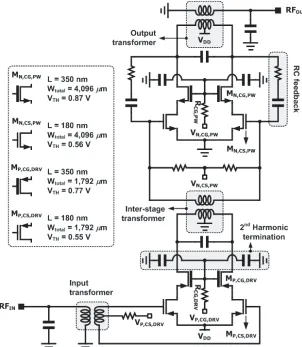
Figure 5 shows the designed CMOS power amplifier. In this study, we select the values of RCG, DRV and RCG, P W as 200 Ω to suppress the IMD3. To avoid oscillation in the designed power amplifier, the RC feedback technique is applied to the power stage of the amplifier. Additionally, a second-harmonic termination technique using an MIM capacitor and bond-wires is applied to the gate nodes of MP, CG, DRV and MN, CG, P W to reduce the asymmetries between the upper and lower IMD3s.
The detailed transistor sizes are displayed in Fig. 5. The input transformer has a 1 : 2 turns ratio
with a 10µm metal width of the primary and secondary windings. The inter-stage transformer has a 2 : 1 turns ratio with a 15µm metal width of the primary and secondary windings. The output transformer has a 1 : 2 turns ratio with 40µm and 25µm metal widths of the primary and secondary windings, respectively. The supply voltage, VDD is 3.3 V.
Figure 6 shows the simulated IMD3s with various values ofRCG. As can be observed from Fig. 6, the extent of the suppression of the IMD3 increases as the value of RCG decreases.
Figure 6. Simulated IMD3. Figure 7. Photograph of the designed CMOS power amplifier.
4. MEASURED RESULTS
Figure 7 shows a chip photograph of the designed CMOS power amplifier with a size of 0.9 mm×2.0 mm, including all the test pads. The power amplifier is designed using a 180-nm RFCMOS process that provides one poly layer and six metal layers. For measurement, the fabricated power amplifier is mounted on an FR4 printed circuit board, and bond-wires are used for the RF input, RF output, various bias voltages, the supply voltage, and ground. For measurement, VDD of the designed power amplifier is selected as 3.3 V.
Figure 8. Measured gain and power-added effi-ciency according to output power with continuous wave signal at 2.42 GHz operation frequency.
Figure 8 shows the measured gain and power-added efficiency (PAE) with a 2.42 GHz continuous wave (CW) signal. As can be observed in Fig. 8, because the load impedances of the MN, CS, P W and
MP, CS, DRV with RCG of 0.2 kΩ are almost identical to those with RCG of 1.0 kΩ, the measured gain and PAE of the power amplifier with an RCG of 0.2 kΩ are almost identical to those with an RCG of 1.0 kΩ. This phenomenon is predicted in the preceding theoretical analysis.
Figure 9 shows the measured lower and upper IMD3s for the RCG values of 0.2 kΩ and 1.0 kΩ. If we set the reference of the IMD3 at −25 dBc, the maximum output power with the RCG of 0.2 kΩ is approximately 0.7 dB higher than that with the RCG of 1.0 kΩ. As predicted in the previous section, the IMD3 with lowered RCG value is successfully suppressed. Fig. 10 shows the measured gain and PAE with a 2.42 GHz 802.11n modulated signal of 20 MHz bandwidth and 64-QAM. Considering the IMD3 reference of−25 dBc, the PAEs at the maximum output power with theRCGvalues of 0.2 kΩ and 1.0 kΩ, are almost identical at 26.7%, as exhibited in Fig. 10. As shown in Fig. 11, the measured EVM is approximately 3.72% at the measured maximum output power of 22.2 dBm of the power amplifier with theRCG of 0.2 kΩ.
The measured results are in satisfactory agreement with the simulation results. As can be predicted from Fig. 4, although the measured gain and PAE of the power amplifier with the RCG of 0.2 kΩ are
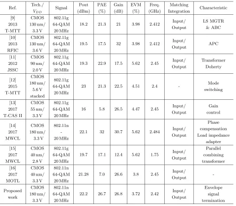
Table 1. Summary and performance comparison of recent CMOS PAs for WLAN.
Ref. Tech./ VDD Signal Pout (dBm) PAE (%) Gain (dB) EVM (%) Freq. (GHz) Matching Integration Characteristic [9] 2013 T-MTT CMOS 130 nm/ 3.3 V 802.11g 64-QAM 20 MHz
18.2 21.3 21 3.98 2.412 Input/ Output LS MGTR & ABC [10] 2013 RFIC CMOS 130 nm/ 3.6 V 802.11g 64-QAM 20 MHz
19.5 17.5 32 3.98 2.412 Input/
Output APC [11] 2012 JSSC CMOS 90 nm/ 2.0 V 802.11g 64-QAM 20 MHz
19.3 22.9 17.5 5.62 2.45 Input/ Output Transformer Doherty [12] 2015 T-MTT CMOS 180 nm/ 5.6 V stacked 802.11g 64-QAM 20 MHz
23 21.3 22.5 4.51 2.4 - Mode switching [13] 2017 T-CAS II CMOS 55 nm/ 3.3 V 802.11g 64-QAM 20 MHz
16 5.8 26.5 4.47 2.45 Input/ Output Gain control [14] 2017 MWCL CMOS 180 nm/ 3.3 V 802.11n -20 MHz
22.1 32 30.7 5.62 2.484 Input/ Output Phase compensation Load impedance adapter [15] 2017 MWCL CMOS 40 nm/ 2.8 V 802.11g 64-QAM 20 MHz
19.7 17.1 12.4 5.62 1.75 Input/ Output Parallel combining transformer [16] 2017 MOTL CMOS 40 nm/ 3.3 V 802.11n 64-QAM 20 MHz
21.28 7.0 26.6 3.8 2.45 Input/
Output -Proposed work CMOS 180 nm/ 3.3 V 802.11n 64-QAM 20 MHz
22.2 26.7 26.8 3.72 2.42 Input/ Output
Figure 10. Measured results: gain and PAE according to output power with 802.11n modulated signal.
Figure 11. Measured results: EVM with 802.11n modulated signal.
almost identical to that with theRCG of 1.0 kΩ, the maximum output power with theRCG of 0.2 kΩ is improved by approximately 0.7 dB compared to that with theRCG of 1.0 kΩ. A change in the value of only RCG resulted in an improvement of 0.7 dB in the maximum linear output power.
Table 1 shows the summary and performance comparison of CMOS power amplifiers for WLAN applications. As can be seen in Table 1, the proposed power amplifier has the lowest measured EVM value and the highest maximum linear output power. Additionally, excluding the results of Ref. [14], the proposed power amplifier has the highest PAE.
5. CONCLUSION
In this study, we have investigated the influence of the envelope impedance of a common-gate transistor with a cascode structure, on the IMD3 of a CMOS power amplifier. We found that the magnitude of the impedance should be reduced to suppress the IMD3. To reduce the magnitude of the impedance of the envelope signal, we regulated the resistance of the bias circuit of the cascode-structure common-gate transistor. From the investigation, the value of the resistance should be minimized to maximize the suppression of the IMD3. However, considering the ESD protection issue and the variation in the bond-wires of the chip-on-board circuits, we concluded that the optimum value of the resistance is around 0.2 kΩ. The salient advantage of the proposed method is that it can be easily applicable to most CMOS power amplifiers without sacrificing other performances such as maximum output power and PAE. To verify the feasibility of the extracted value of the resistance of the bias circuit of the common-gate transistor of the amplifier, we designed a power amplifier using a 180-nm RFCMOS process for WLAN 802.11n applications. We obtained the measured maximum linear output power of 22.2 dBm with a 26.7% power-added efficiency and a 3.72% error vector magnitude. We used an 802.11n modulated signal with 64-QAM (MCS7) at 65 Mb/s. From the measured results, we successfully verified the feasibility of the proposed optimization technique of the resistance of the bias circuit of the common-gate transistor.
ACKNOWLEDGMENT
This research was supported by the Basic Science Research Program through the National Research Foundation of Korea (NRF), funded by the Ministry of Science, ICT & Future Planning (2015-036938).
REFERENCES
2. Jeong, G., T. Joo, and S. Hong, “A highly linear and efficient CMOS power amplifier with cascode-cascade configuration,”IEEE Microw. Wirel. Compon. Lett., Vol. 27, 596–598, 2017.
3. Kang, S., G. Jeong, and S. Hong, “Study on dynamic body bias controls of RF CMOS cascode power amplifier,” IEEE Microw. Wirel. Compon. Lett., Vol. 28, 705–707, 2018.
4. Kang, S., D. Baek, and S. Hong, “A 5-GHz WLAN RF CMOS power amplifier with a parallel-cascoded configuration and an active feedback linearizer,” IEEE Trans. Microw. Theory Techn., Vol. 65, 3230–3244, 2017.
5. Park, J., C. Lee, and C. Park, “A quad-band CMOS linear power amplifier for EDGE applications using an anti-phase method to enhance its linearity,” IEEE Trans. Circuits Syst. I — Regul. Pap., Vol. 64, 765–776, 2017.
6. Park, J., C. Lee, J. Yoo, and C. Park, “A CMOS antiphase power amplifier with an MGTR technique for mobile applications,”IEEE Trans. Microw. Theory Techn., Vol. 65, 4645–4656, 2017. 7. Jin, S., M. Kwon, K. Moon, B. Park, and B. Kim, “Control of IMD asymmetry of CMOS power amplifier for broadband operation using wideband signal,” IEEE Trans. Microw. Theory Techn., Vol. 61, 3753–3762, 2013.
8. Jung, S.-C., et al., “A new envelope predistorter with envelope delay taps for memory effect compensation,” IEEE Trans. Microw. Theory Techn., Vol. 55, 52–59, 2007.
9. Joo, T., B. Koo, and S. Hong, “A WLAN RF CMOS PA with large signal MGTR method,”IEEE Trans. Microw. Theory Techn., Vol. 61, 1272–1279, 2013.
10. Joo, T., B. Koo, and S. Hong, “A WLAN RF CMOS PA with adaptive power cells,”Proc. IEEE RFIC Symp., 345–348, Seattle, WA, USA, 2013.
11. Kaymaksut, E. and P. Reynaert, “Transformer based uneven Doherty power amplifier in 90 nm CMOS for WLAN applications,” IEEE J. Solid-State Circuits, Vol. 47, 1659–1671, 2012.
12. Yin, Y., X. Yu, Z. Wang, and B. Chi, “An efficiency-enhanced stacked 2.4-GHz CMOS power amplifier with mode switching scheme for WLAN applications,” IEEE Trans. Microw. Theory Techn., Vol. 63, 672–682, 2015.
13. Jeong, G., S. Kang, T. Joo, and S. Hong, “An integrated dual-mode CMOS power amplifier with linearizing body network,”IEEE Trans. Circuits Syst. II, Exp. Briefs, Vol. 64, 1037–1041, 2017. 14. Jin, Y. and S. Hong, “A 2.4-GHz CMOS common-gate combining power amplifier with load
impedance adaptor,”IEEE Microw. Wirel. Compon. Lett., Vol. 27, 836–838, 2017.
15. Ahn, H., S. Baek, I. Nam, D. An, J. K. Lee, M. Jeong, B.-E. Kim, J. Choi, and O. Lee, “A fully integrated dual-mode CMOS power amplifier with an autotransformer-based parallel combining transformer,”IEEE Microw. Wirel. Compon. Lett., Vol. 27, 833–835, 2017.