A High-Swing Class-C VCO with Amplitude Feedback Loop for Low
Phase Noise and Robust Start-up
Qi Liu1, 2, *, Ye-Bing Gan1, and Tian-Chun Ye1
Abstract—A novel high-swing Class-C VCO with an amplitude feedback loop is presented. The amplitude feedback loop is used to ensure the start-up of the VCO which also makes the proposed VCO always have an optimal phase noise against the PVT variations automatically. The proposed circuit is implemented in a 65 nm CMOS process. The VCO has exhibited a measured phase noise of −128.6 dBc/Hz at 1 MHz offset from the 1.52 GHz carrier frequency with a 1.4 mW power consumption. The variation of measured phase noise at 1 MHz offset is less than 2.3% while temperature changes from −40◦C to 100◦C.
1. INTRODUCTION
The availability of Voltage Control Oscillator (VCO) with low phase noise at low power consumption is of primary importance in both wireless and wired communications. For this reason, an oscillator architecture known as a Class-C harmonic VCO is popular in the last years [1–7]. The Class-C VCO takes advantages of biasing cross-coupled transistors in a Class-C condition, resulting in more efficient generation of oscillation currents from DC bias current. A theoretical 3.9 dB phase noise improvement compared to the standard differential-pair LC-tank oscillator is achieved for the same current consumption [1]. Though the Class-C VCO seems a perfect topology, it still has some drawbacks. For instance, the maximum oscillation amplitude of Class-C VCO is limited by the value of gate bias voltage Vgbias since the switching pair should not operate in the deep triode region. It is well know that lager oscillation amplitude always leads to better phase noise based on Leeson’s phase noise equation [8]. Therefore, a lower gate bias voltageVgbias is required for enhancing the maximum oscillation amplitude and improving the phase noise. On the other hand, the Class-C VCO is difficult to start up with a lower gate bias voltage. Commonly, the traditional Class-C VCO prefers to use a high gate bias voltage to ensure robust start-up against Process Voltage Temperature (PVT) variations compared to using a low gate bias voltage.
To break the trade-off between robust start-up and phase noise, a Class-C VCO with an amplitude feedback loop for low phase noise and robust start-up is proposed in this paper. The topology of a conventional Class-C VCO is modified for higher oscillation amplitude under a low supply voltage. This high-swing Class-C VCO with an amplitude feedback loop is implemented in 65 nm CMOS process.
2. DESIGN OF THE VCO CIRCUITS
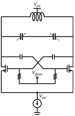
A conventional Class-C VCO is shown in Fig. 1. As transistors must work in the active region to keep the Class-C operating. The well-know saturation condition, VDS >VGS−Vth, should be satisfied at
Received 18 July 2019, Accepted 29 August 2019, Scheduled 20 September 2019
* Corresponding author: Qi Liu ([email protected]).
Vdd
Vgbias
Vtail
Figure 1. Simplified structure of a conventional Class-C VCO.
Vdd
Vgbias2
Figure 2. High-swing Class-C VCO.
any moment after the Class-C VCO begins to oscillate. The most critical situation is when VDS is minimum and VGS maximum:
Vdd−Atank−Vtail > Vgbias+Atank−Vtail−Vth (1) Eq. (1) indicates that the limit value of the oscillation amplitude is:
Atank<
Vdd−Vgbias+Vth
2 (2)
Eq. (2) demonstrates the relationship between the gate bias voltage Vgbias and oscillation amplitude Atank more directly. It can be seen that there are two ways to increase the oscillation amplitude. One is to increase the supply voltage Vdd, and the other is to reduce the gate bias voltage Vgbias. As the supply voltage Vdd is always limited by the CMOS process or the requirement of system, the only way to improve the oscillation amplitude is to decrease the gate bias voltage Vgbias.
2.1. The Topology of High-Swing Class-C VCO
As mentioned above, the only way to acquire higher oscillation amplitude is reducing the gate bias voltage. It is a challenging task for the traditional Class-C VCO. In order to provide higher voltage headroom for oscillation amplitude, the tail transistor is removed in the topology of high-swing Class-C VCO. Fig. 2 illustrates the simple circuit of high-swing Class-C VCO [9–11].
Likewise, by using the saturation condition to analyze the high-swing Class-C VCO as well, the limit expression of oscillation amplitude can be concluded as follows:
Atank<
Vdd−Vgbias2+Vth
2 (3)
There seems no difference between Eq. (2) and Eq. (3). In fact, Vgbias2 differs from Vgbias. In the conventional Class-C VCO, the gate bias voltage should be:
Vgbias=Vtail+Vth+Vod (4)
However, in a high-swing Class-C VCO, the gate bias voltage is:
Here Vod represents the over-drive voltage of the transistor. Comparing Eq. (4) with Eq. (5), it is easy to see that the gate bias voltage in the high-swing Class-C VCO has been reduced byVtail. Therefore, the oscillation amplitude of high-swing Class-C VCO is improved by Vtail/2 which is worthwhile in low voltage design.
Although removing the tail transistor can enhance the oscillation amplitude, it also brings a problem. The problem is that the transconductance (gm) of transistor becomes more sensitive to PVT variations. Such big variations of the small signal gm make the high-swing Class-C VCO hardly have a robust start-up against PVT variations. An auxiliary circuit is designed to solve this problem in this work, and the details are described in the next paragraph.
2.2. Proposed High-Swing Class-C VCO with Amplitude Feedback Loop
As mentioned above, high-swing Class-C VCO makes the start-up more difficult against PVT variations. Generally, the small signal transconductance of transistor is made several times higher than gm to ensure robust start-up of a VCO [12]. In the high-swing Class-C VCO, the small signal transconductance of transistor is determined by the gate bias voltage:
gm =K· W
L ·(VGS−Vth) (6)
which means that a higher small signal transconductance needs a higher gate bias voltage. This requirement of gate bias voltage for robust start-up is contrary to that for low phase noise performance. To resolve this contradiction, a high-swing Class-C VCO with amplitude feedback loop is proposed in this paper.
Figure 3 depicts the schematic of the proposed VCO. The oscillation amplitude is monitored by an amplitude detector which consists of M3, M4, and C1. Unity gain amplifier plays a role of isolator, eliminating a part of noise from the amplitude detector. Then a operation unit consists of an amplifier and two resistors will generate a voltage signal according to the value of Vb and the result of amplitude detector which is the same asVa. The signal then filtered by an RC low-pass network before is transmitted to the gates of M1 and M2. The low-pass filter here serves to filter out unwanted noise from the feedback loop. More detailed operation principle of the amplitude feedback loop is discussed latter.
As the proposed VCO is a Class-C VCO, the analysis used for the conventional Class-C VCO is still useful for the proposed VCO. Then, the critical condition to guarantee M1 and M2 to work in
Vdd
Amplitude detector
Operation Unit
M1 M2
M3 M4
R1 R2
Va
Vb
Vdd
C1
Isolator
active regions can be derived from Eq. (2):
Atank=
Vdd−Vgbias+Vth
2 (7)
which can be changed to:
Vgbias=Vdd−2·Atank+Vth= 2·(Vdd−Atank)−(Vdd−Vth) (8) Eq. (8) indicates that if a gate bias voltage is equal to the right-hand expression in Eq. (8), an excellent phase noise can be provided. It is quite appealing since the phase noise is very important in a VCO. Then, the operation unit in the amplitude feedback loop will be illustrated. It consists of an amplifier and several resistors. Set R1 equal to R2, and regard the amplifier as an ideal amplifier. Then, by using the Kirchhoff’s law, it is concluded that the output of the operation unit is:
Vout = 2·Va−Vb (9)
As the expression in Eq. (9) is similar to that in Eq. (8), only two voltages that equalVdd−Atank and Vdd−Vth respectively need to be found. As shown in Fig. 3,Vais generated by the amplitude detector. Actually, the amplitude detector detects the negative envelop of the VCO while the VCO is oscillating. And the output of amplitude detector is slightly higher than the negative envelop of the VCO. The simulation result of the amplitude detector is depicted in Fig. 4.
500 550 600 650 700 750 800 850 900
Time (ns) 1.3 1.2 1.1 1.0 0.9 0.8 0.7 0.6 0.5 Voltage (V) V dd V V V on op out
Figure 4. Simulation result of amplitude detector. 0.8 0.7 0.6 0.5 0.9 0.3 0.2 0.1 0.0 0.4
V (V)gd_max
-122 -123 -124 -125 -126 -127 -128 -129 -130 -131 -132
Phase Noise @ 1 MHz (dBc/Hz)
Vth
Figure 5. Simulate phase noise @1 MHz at different value ofVgd.
As can be seen in Fig. 4, the output of amplitude detector which is also equal toVacan be written as:
Va=Vout=Vdd−Atank+Verror (10)
IgnoreVerror for a while, a voltage same asVdd−Atank is obtained. Now, a voltage that equalsVdd−Vth to implement the gate bias voltage still needs to be found. This voltage is simply generated by the circuits shown in Fig. 3. The value of Vb can be quickly derived from the current characteristic of a transistor:
Vb =Vdd−Vth−
2I K ·
L
W (11)
from the output of operation unit to the gate of transistors. By using Eq. (9), Eq. (10), and Eq. (11), the gate bias voltage of transistors can be expressed as:
Vgbias=Vout = 2·(Vdd−Atank)−(Vdd−Vth) + 2·Verror+
2I K ·
L
W (12)
The last two items in Eq. (12) make the gate bias voltage exceed the critical condition for transistor to work in active regions. It also means that the couple of transistors may moderately enter the triode region. This seems a bad news as those items may break the condition for transistor to work in active regions. However, Mazzanti and Andreani have proven that no phase noise deterioration occurs as long as the couple of transistor does not enter the triode region deeply [1]. In fact, the simulation result of phase noise against different Vgd in Fig. 5 even illustrates that the Class-C VCO has the best phase noise while the couple of transistors slightly enters the triode region. This changes the last two items in Eq. (12) from bad to good. The best phase noise can be achieved through setting the current I and the ratio of W/L appropriately. All in all, an amplitude feedback loop is used to make the couple of transistors moderately enter the triode region, which guarantees the best phase noise at any time.
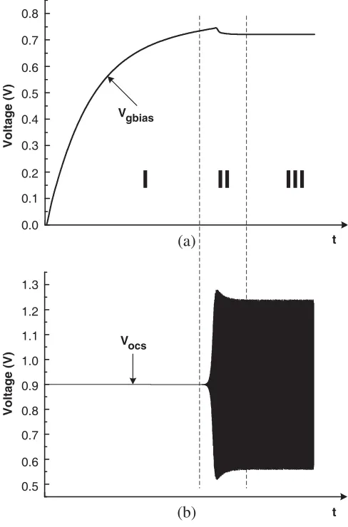
The effect of the amplitude feedback loop on phase noise has been discussed. The focus of this work will be on the robust start-up of the VCO. Detailed analysis is performed to demonstrate the feasibility of the proposed feedback high-swing Class-C VCO with robust start-up. A transient simulation is performed to confirm the effectiveness of the proposed approach. As can be seen in Fig. 6, the VCO
(a)
(b) 1.3
1.2
1.1
1.0
0.9
0.8
0.7
0.6
0.5
Voltage (V)
0.8
0.7
0.6
0.5
0.3
0.2
0.1
0.0 0.4
Voltage (V)
t t
Vgbias
Vocs
I
II
III
does not oscillate at first. Therefore, the drain voltage and gate voltage of M3 and M4 are both Vdd, which means that M3 and M4 are both turned on. Then, the output voltage of amplitude detector which is the same asVabegins to increase, and the output of operation unit will also increase, sinceVa increases, andVbremains unchanged, resulting in increase of the gate bias voltages of M1 and M2 at the same time. The increased gate bias voltages lead to a small signal transconductance increase. Once the start-up condition is satisfied, the VCO begins to oscillate. AsVa can be as high asVdd if the oscillator never oscillates, the output of the operate unit can also be as high as Vdd from Eq. (9) and Eq. (11). It means that the gate bias voltage of transistor can reach Vdd. This makes the high-swing Class-C VCO free from the problem of start-up against the PVT variations. Once the VCO begins to oscillate, the increased oscillation amplitude would decrease the gate bias voltage through the feedback loop. At the end of the transient, the feedback loop ensures an appropriate voltage at the gates of M1 and M2, which allows the couple of transistors enter the triode region slightly for the best phase noise. Fig. 6 shows the transient simulation results ofVgbias and Vosc (output of VCO), and the transient simulation result can be divided into three parts as can be seen in Fig. 6. During Part I, Vgbias keeps rising until the VCO begins to oscillate. Then Vgbias is adjusted by the oscillate amplitudeAtank which is indicated in Eq. (12) in Part II. Finally, Vgbias becomes stable in Part III. Such a transient simulation result quite well agrees with the theoretical analysis discussed above, which proves that amplitude feedback loop is effective.
2.3. Consideration of the Proposed Design
Now, consider the design of amplifiers in the feedback loop. One amplifier is used to form a voltage follower which can provide necessary isolation between the output of amplifier detector and input of operation unit, and the other amplifier is used to form a voltage operation circuit which can give an appropriate Vgbias. The amplifiers should be a rail to rail amplifier as the input voltage of voltage follower and output of the amplitude detector, which are ranged from 0 to Vdd. The specification of the amplifier is relaxed except for the input voltage range. Since the output of amplifier detector is nearly DC signals when the feedback loop is settled, the bandwidth of amplifier is relaxed. However, the output of amplifier detector still has some low frequency components while the feedback loop is not settled. A very narrow bandwidth may lead to instability in the oscillation amplitude. To prevent this undesirable instability, the amplifier employed in this design is required to have a bandwidth of several tens of MHz. As for the gain of amplifier, higher gain means that the output of voltage follower and operation unit are more precise, and it is hoped in this design that the gain can be as high as possible under limited power consumption and layout area. Thus, a constant gm structure is adopted to realize the rail-to-rail high gain amplifier. The requirements of gain flatness are loose because more attention is paid to the minimum gain of the entire input voltage range. In this work, a constant gm structure rail-to-rail amplifier provides a 70 dB DC gain over the entire input voltage range with a 11 MHz bandwidth being adopted.
The transistors in amplitude detector directly connect to the output of VCO. Small ratio should be used to avoid influencing the operation of VCO. In this work, the W/L of M3 and M4 is 1µm/60 nm. The value of capacitor C1 should be selected carefully. A small C1 may have a fast start-up time and a small layout area, but a bigger C1 can filter the ripple more efficiently and have a small error in Eq. (10). In this work, a 1 pF MOM capacitor is used to filter the ripple and save area.
3. MEASUREMENT RESULT
The proposed high-swing Class-C VCO with amplitude feedback loop is implemented in a standard 65 nm CMOS process. A micrograph of the proposed circuit is shown in Fig. 7. The area of VCO is 550µm∗380µm, and the area of the amplitude feedback loop is 170µm∗110µm. The total area of the proposed circuit is 0.23 mm2 (without the output buffs). The VCO oscillation frequency, output power, and the phase noise are measured by an Agilent N9020A MXA signal analyzer.
High swing class-C VCO
Amplitude Feedback Loop
Figure 7. Chip micrograph of the proposed circuit.
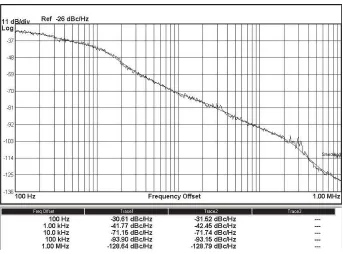
Figure 8. Measured output spectrum.
the frequency tuning range is from 1.45 GHz to 1.64 GHz. The proposed VCO gets a quite low phase noise even uses a 0.9 V supply voltage owning to the high-swing Class-C VCO. All the measurements mentioned above are performed at room temperature.
Figure 10 illustrates the measured phase noise at an offset of 1 MHz from the carrier frequency while temperature changes from−40◦ to 100◦. As the data of measured phase noise at any temperature have been obtained, it also means that the proposed VCO with an amplitude feedback loop displays robust start-up over the entire temperature range of −40◦ to 100◦. This demonstrates that the amplitude feedback loop has solved the start-up problem of the high-swing Class-C VCO successfully. As can be seen in Fig. 10, the measured phase noise varies less than 2.3% over the entire temperature range.
Figure 9. Measured phase noise of the proposed VCO.
-125
-126
-127
-128
-129
-130
-131
-132
Phase Noise @ 1 MHz (dBc/Hz)
-133
-134
-135
-40 -20 0 20 40 60 80 100
Temperature ( C)O
Figure 10. Measured phase noise @1 MHz against temperature.
different frequencies and power dissipations is adopted [13]:
FOM =ζ(foffset)−20 log
f
osc foffset
+ 10 log
P
vco 1 mW
(13)
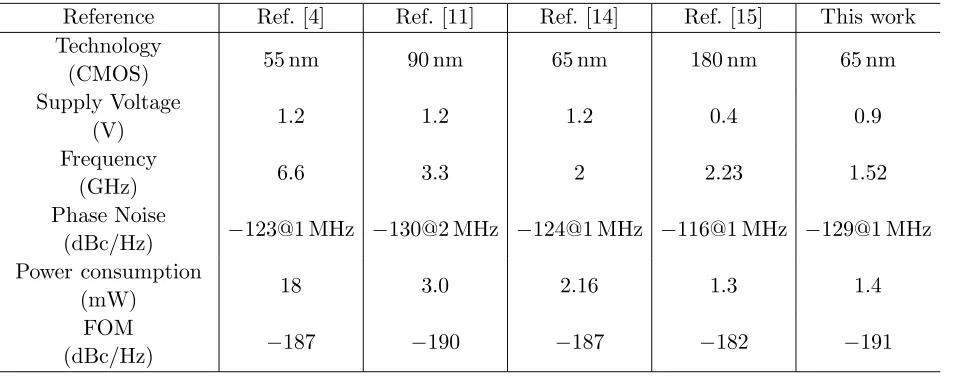
Table 1. Comparison of recently published LC-VCOs and this work.
Reference Ref. [4] Ref. [11] Ref. [14] Ref. [15] This work
Technology
(CMOS) 55 nm 90 nm 65 nm 180 nm 65 nm
Supply Voltage
(V) 1.2 1.2 1.2 0.4 0.9
Frequency
(GHz) 6.6 3.3 2 2.23 1.52
Phase Noise
(dBc/Hz) −123@1 MHz −130@2 MHz −124@1 MHz −116@1 MHz −129@1 MHz
Power consumption
(mW) 18 3.0 2.16 1.3 1.4
FOM
(dBc/Hz) −187 −190 −187 −182 −191
4. CONCLUSION
A high-swing Class-C VCO with an amplitude feedback loop is presented in this paper. The structure of high-swing Class-C VCO improves the oscillation amplitude of Class-C VCO under low supply voltage. The amplitude feedback loop is used to achieve a robust start-up and adjust the operation point for the minimum phase noise against the PVT variations automatically. With careful design, the proposed VCO is suitable for low phase noise PVT-robust Phase Lock Loops (PLLs) with low supply voltage.
REFERENCES
1. Mazzanti, A. and P. Andreani, “Class-C harmonic CMOS VCOs, with a general result on phase noise,” IEEE J. Solid-State Circuits, Vol. 43, 2716, 2008, DOI: 10.1109/JSSC.2008.2004867. 2. Chen, J., et al., “A low power, startup ensured and constant amplitude Class-C VCO in
0.18µm CMOS,” IEEE Microwave & Wireless Components Letters, Vol. 21, 427, 2011, DOI: 10.1109/LMWC.2011.2160620.
3. Fanori, L. and P. Andreani, “Highly efficient Class-C CMOS VCOs, including a com-parison with class-B VCOs,” IEEE J. Solid-State Circuits, Vol. 48, 1730, 2013, DOI: 10.1109/JSSC.2013.2253402.
4. Perticaroli, S., et al., “A harmonic Class-C CMOS VCO-based on low frequency feedback loop: Theoretical analysis and experimental results,”IEEE Trans. Circuits Syst. I, Reg. Papers, Vol. 61, 2537, 2014, DOI: 10.1109/TCSI.2014.2332268.
5. Zhu, Z., et al., “A startup robust feedback Class-C VCO with constant amplitude control in 0.18µm CMOS,” IEEE Microwave & Wireless Components Letters, Vol. 25, 541, 2015, DOI: 10.1109/LMWC.2015.2440871.
6. Li, C. and A. Liscidini, “Class-C PA-VCO cell for FSK and GFSK transmitters,” IEEE J. Solid-State Circuits, Vol. 51, 1537, 2016, DOI: 10.1109/JSSC.2016.2554148.
7. Song, J. H., et al., “An adaptively biased Class-C VCO with a self-turn-off auxiliary Class-B pair for fast and robust startup,” IEEE Microwave & Wireless Components Letters, Vol. 26, 34, 2016, DOI: 10.1109/LMWC.2015.2505637.
8. Leeson, D. B., “A simple model of feedback oscillator noise spectrum,” Proceedings of the IEEE, Vol. 54, 329, 1966, DOI: 10.1109/PROC.1966.4682.
10. Ataei, F. and M. Yavari, “A 2.2 GHz high-swing Class-C VCO with wide tuning range,”MWSCAS, 1, 2011, DOI: 10.1109/MWSCAS.2011.6026276.
11. Fanori, L. and P. Andreani, “A high-swing complementary Class-C VCO,” ESSCIRC, 407, 2013, DOI: 10.1109/ESSCIRC.2013.6649159.
12. Jansen, S., et al., “Silicon bipolar VCO family for 1.1 to 2.2 GHz with fully-integrated tank and tuning circuits,” ISSCC Dig. Tech. Papers, 392, 1997, DOI: 10.1109/ISSCC.1997.585455.
13. Kim, J., et al., “A wide-band CMOS LC VCO with linearized coarse tuning characteristics,” IEEE Trans. Circuits Syst. II, Exp. Briefs, Vol. 55, 399, 2008, DOI: 10.1109/TCSII.2007.914896.
14. Li, X., et al., “New design method of LC VCO improving PVT tolerance of phase noise,”Chinese Journal of Electronics, Vol. 24, 550, 2015, DOI: 10.1049/cje.2015.07.019.