STELLAR: A Generic EM Side-Channel Attack
Protection through Ground-Up Root-cause Analysis
Debayan Das
1, Mayukh Nath
1, Baibhab Chatterjee
1, Santosh Ghosh
2, Shreyas Sen
1 1School of Electrical and Computer Engineering, Purdue University, USA
2
Intel Labs, Hillsboro, Oregon, USA
{das60, nathm, bchatte, shreyas}@purdue.edu, [email protected]
Abstract—The threat of side-channels is becoming increasingly prominent for resource-constrained internet-connected devices. While numerous power side-channel countermeasures have been proposed, a promising approach to protect the non-invasive electromagnetic side-channel attacks has been relatively scarce. Today’s availability of high-resolution electromagnetic (EM) probes mandates the need for a low-overhead solution to protect EM side-channel analysis (SCA) attacks. This work, for the first time, performs a white-box analysis to root-cause the origin of the EM leakage from an integrated circuit. System-level EM simulations with Intel 32 nm CMOS technology interconnect stack, as an example, reveals that the EM leakage from metals above layer 8 can be detected by an external non-invasive attacker with the commercially available state-of-the-art EM probes. Equipped with this ‘white-box’ understanding, this work proposesSTELLAR: Signature aTtenuation Embedded CRYPTO with Low-Level metAl Routing, which is a two-stage solution to eliminate the critical signal radiation from the higher-level metal layers. Firstly, we propose routing the entire cryptographic core within the local lower-level metal layers, whose leakage cannot be picked up by an external attacker. Then, the entire crypto IP is embedded within a Signature Attenuation Hardware (SAH) which in turn suppresses the critical encryption signature before it routes the current signature to the highly radiating top-level metal layers. System-top-level implementation of the STELLAR hardware with local lower-level metal routing in TSMC 65 nm CMOS technology, with an AES-128 encryption engine (as an example cryptographic block) operating at 40 MHz, shows that the system remains secure against EM SCA attack even after1M
encryptions, with67%energy efficiency and1.23×area overhead compared to the unprotected AES.
Index Terms—EM Side-channel attack, Generic countermea-sure, Ground-up EM Leakage Modeling, Cryptographic hard-ware, STELLAR, Signature Attenuation Hardware
I. INTRODUCTION
The huge growth of internet-connected devices has led to the development of strong and mathematically-secure crypto-graphic algorithms. Almost all embedded devices including mobile phones and smart cards employ encryption engines. However, unfortunately these algorithms are implemented on a physical platform, and these physical CMOS-based devices leak information in the form of power consumption [1], [2], electromagnetic (EM) emanations [3], [4], acoustic vibra-tions [5] or the timing of encryption operavibra-tions [6]. These side-channel leakage information can be exploited by attackers to extract the secret key from an encryption device.
This work was supported in part by the National Science Foundation (NSF) under Grant CNS 17-19235, and in part by Intel Corporation.
Fig. 1. EM Side-Channel attack Overview.
A. Preliminaries
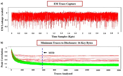
The EM analysis attack is a prominent non-invasive side-channel attack (SCA) on cryptographic ICs and has been demonstrated over the last decade [7], [8]. The EM analysis attack is typically performed in two phases. In the first phase, the attacker collects the EM emanations using an EM probe optionally connected to a low-noise amplifier (LNA) placed in the vicinity of the encryption device under attack. In the second phase, the collected EM traces are subjected to simple (SEMA) or differential EM analysis (DEMA) [9] to extract the secret key of the encryption device.
at each sampling point of the trace. The key byte showing the maximum correlation represents the correct key byte. Repeating the process 16 times reveals the entire 128 bits of the secret key.
Real-world examples of EM SCA include the counterfeiting of e-cigarette batteries by stealing the secret encryption keys from the authentic batteries to gain market share. In general, electromagnetic analysis attacks can be used to extract the hidden key from the boot-loader of any embedded VLSI device [7], [8], [11].
B. Motivation
Power and EM SCA attacks on encryption ICs have gained tremendous importance over the last decade [12], [13], [11], [14]. Although researchers have mainly focused on countermeasures against power SCA, preventing EM attacks is gaining more prominence in the present era of IoT, due to the availability of commercial inexpensive EM probes. Being in the close proximity of the encryption device, the EM side-channel leakage can be captured non-invasively using low-cost EM probes, in contrast to the requirement for physical probing in power analysis attacks. Hence, a low-overhead generic countermeasure that can be commonly utilized for both power and EM side-channel resilience is extremely necessary.
This work performs a ground-up analysis to root-cause the origin of the EM leakage in an integrated circuit (IC). After identifying the source of the EM leakage, we investigate the existing state-of-the-art power and EM SCA countermeasures that can be utilized for protecting the cryptographic IC. Among the existing countermeasures, the recently proposed Attenu-ated Signature Noise Injection (ASNI) [15] is a generic and low-overhead solution to protect against power SCA. In this work, we propose STELLAR: Signature aTtenuation
Em-bedded CRYPTO with Low-Level metAl Routing, utilizing
Signature Attenuating Hardware (SAH) to embed the entire cryptographic IP of an electronic system with local low-level metal routing and thereby significantly attenuate the signature before it reaches the top metal layers of the chip, which leaks critical information through EM side-channels.
In this article, as an application of the proposed counter-measure, we focus on a 128-bit AES engine. Correlational EM analysis (CEMA) with Hamming distance (HD) model [10] is employed for the attack.
C. Contribution
Specific contributions of this paper are:
• This work, for the first time, performs a ground-up root-cause analysis to develop the fundamental understanding, i.e. a ‘white-box model’ of thekey source of EM informa-tion leakagefrom the current path of a cryptographic IC. System-level simulations using Ansoft HFSS for 32 nm Intel CMOS technology, as an example, reveals that EM leakage is detectable using state-of-the-art commercial probes from metal layers only higher than 8.
• To eliminate the critical signature radiation from the
higher-level metal layers, a two-stage solution, named
STELLAR, is proposed. (1) Electromagnetic field Sup-pression: The cryptographic IP is routed through the local lower-level metal layers, reducing EM leakage. However, due to its high routing resistance, low-level routing could only be local and cannot be routed to the metal pads of the chip. This calls for the (2) Signature Suppression: The encryption signature needs to be highly suppressed, using local circuity that embeds the sensitive CRYPTO block inside it, before the current signature is routed to the global higher metal layers. A combined effect of Local EM field Suppression and the Global Signature Suppression is the key to minimizing EM side-channel leakage.
• In order to suppress the AES encryption (or the whole
cryptographic core in general) signature, STELLAR uti-lizes a Signature Attenuating Hardware (SAH), such as Attenuated Signature Noise Injection (ASNI) [15], to at-tenuate the correlated AES current signature significantly before it reaches the higher metal layers, thereby enabling EM as well as power SCA immunity.
• CEMA attacks implemented on the STELLAR-AES with local lower-level metal routing show that none of the secret key blocks have been disclosed even with 1M
traces (Minimum Traces to Disclosure (MTD) > 1M), with only 1.23× area overhead, 1.5× power overhead compared to the unprotected AES, and moreover,without any performance penalty.
II. BACKGROUND& RELATEDWORK
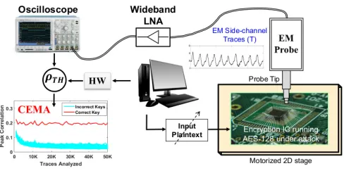
Our EM SCA attack set-up involves a target Atmega mi-crocontroller (using the Chipwhisperer platform) [16] running AES-128 encryption, and the EM field is picked up by a nearby EM probe connected to a low-noise amplifier (LNA) and captured using an oscilloscope. The oscilloscope data is then downloaded to a PC wherein the correlation EM analysis (CEMA) is performed to reveal each byte of the secret key. As
2000 1800 1600 1400 1200 1000 800 600 400 200 0 1 0.8 0.6 0.4 0.2
0
-0.2 -0.1 0
3 2.8 2.6 2.4 2.2 2 1.8 1.6 1.4 1.2 1 0.8 0.6 0.4 0.2 0
EM Trace Capture
MTD
Traces Analyzed
Peak
C
orrel
at
ion
Time Samples (Kpts)
E
M
L
ea
k
ag
e (scal
ed
)
Minimum Traces to Disclosure: 16 Key Bytes
a)
b)
seen from Figure 2(a, b), all the 16 key bytes of the AES-128 implementation can be obtained within <600traces, thereby breaking the security of this system. Although this is a basic example to prove the feasibility of EM SCA, it demonstrates the potency of EM SCA attacks on electronic systems.
A. Literature Review: Black Box Approach
Several EM side-channel attacks have been demonstrated over the last few years. In CHES 2002 [17], it was first shown that the EM spectrum could be sensed to perform SCA. There have been few works to scan the EM emissions of integrated circuits in time-domain [18]. Lomne et al. [19] proposed a modeling of magnetic emissions from ICs using Redhawk. Recently, Kumar et al. [20] proposed an efficient simulation set-up to perform EM SCA. However, most of these works focus on top-down modeling of EM emissions from a chip and consider the cryptographic IC as a black box. In CHES 2014 [21], the authors developed an on-chip sensor to detect an approaching probe. In addition, the development of highly sensitive EM probes [7] calls for a fundamental understanding of the characteristics of EM side-channel leakage from crypto-graphic ICs and trace the critical information-leakage sources in the current path.
Specific countermeasures proposed against EM SCA in-clude signal strength reduction techniques like shielding or signal information reduction using noise insertion [17]. How-ever, data randomization with noise injection comes with significant power overheads, and EM shielding incurs high cost of packaging [22] and is not a practical solution for most applications. To the best of the authors’ knowledge, none of these works have thoroughly investigated the root-cause of the EM leakage in a cryptographic IC.
B. Genesis of the EM Leakage: A White box Approach
Although the source of leakage in the case of power analysis attack is well understood and analyzed [12], [23], [24], the origin of EM leakage in the context of side-channel security is still not well-perceived. In this work, we conceive a ground-up approach to analyze and root-cause the genesis of this EM side-channel leakage in a CMOS IC.
For an integrated CMOS-based circuit, in steady-state, there is no static current flowing through the circuit. However, the presence of stationary charges in the circuit give rise to electric fields (E~), as can be explained from Gauss’ Law (∇ ·E~ =ρ). As the output of logic gates switches its state, moving charges (dynamic and leakage currents) create changing electric fields, which in turn produce magnetic fields (known as modified
Ampere’s law: ∇ ×H~ = J~ +∂E~
∂t). On the other hand,
changing currents (acceleration of charges) produce time-changing magnetic flux, thereby inducing an electric field,
which is known as the Faraday’s law (∇ ×E~ = −µ∂∂tH~). Note that E~ represents the electric field in V/m,H~ denotes the magnetic field intensity in A/m,B~ represents the magnetic field intensity in Tesla (T), J~is the electric current density in A/m2,ρdenotes the electric charge density in C/m3,is the
Metal 9 Cu Bump
M₁ to M₈ Stack
5 µm 500 nm
a) b)
Fig. 3. Cross-Section of the Interconnect Stack (Intel32 nm) [25], (a) Metal 1 through 8 (b) Includes metal 9 and the copper bump layer.
TABLE I
PITCH AND THICKNESS OF METAL LAYERS ATINTEL’S32NM NODE[25]
Layer Pitch(nm) Thickness(nm)
Metal 1 112.5 95
Metal 2 112.5 95
Metal 3 112.5 95
Metal 4 168.8 151
Metal 5 225.0 204
Metal 6 337.6 303
Metal 7 450.1 388
Metal 8 566.5 504
Metal 9 19.4µm 8µm
Bump 145.9µm 25.5µm
electric permittivity andµis the magnetic permeability of the medium.
The present day CMOS architecture consists of a cell-level transistor layer over a silicon substrate, and multiple layers of metal consisting of interconnects and vias [25]. Depending on different CMOS technologies, the number of total metal layers may vary. However, having more number of metal layers is important for integrated circuit design as it not only makes it easier for the circuit designer, but also reduces the area of the chip significantly as the layers are stacked on top of another. The highest metal layers available for a process are used as the power grid. Hence, any signal in the lower-level metal layers has to be routed to the topmost metal layer and through to the copper (Cu) bump, as shown in Figure 3(b).
As a result, any cell-level excitation is reflected as a time-varying current through the metal layer routings. The interconnects in the routing, due to the presence of this time-varying current, start functioning as antennas, and emit elec-tromagnetic radiation. Now, the typical operating frequency (f) of industrial digital CMOS circuits lie in the 1-10 GHz range, which corresponds to a wavelength (λ= vf,v denotes the speed of propagation of the EM waves and is equal
to 3 ∗ 108m/sec), which is in the order of 30-300 mm,
half wavelength (λ/2) dipole antenna, where the excitation frequency matches the antenna resonance, and the current distribution forms nodes and anti-nodes along the length of the antenna. Now, as the current distribution in an infinitesimal dipole is uniform, it can be intuitively broken down into unit elements, wherein each element contributes equally (Ei) towards the net radiated electric field amplitude Erad. If N
is the number of elements, Erad = N Ei, and as a matter of fact, N is proportional to the dimensions of the radiation structure. As a result, the radiated field amplitude should have a linear dependence on the dimensions of the structure, e.g. if the length of the structure is l, N ∝l and Erad ∝N, so Erad∝l.The radiated powerPradwould then be proportional
tol2. In fact, for infinitesimal dipoles, the radiated power can
be shown to be proportional to(l/λ)2, as given by Eqn. 1 [26],
Prad=η
π
3
I0l λ
2
(1)
whereη=pµ/.
Thus in essence, the time-varying electric and magnetic fields produce an EM wave during the switching activity of the logic and sequential circuits within an ASIC. A nearby attacker can pick up the radiated “side-channel” EM emissions and extract the secret key from the encryption engine using CEMA/DEMA. It is therefore essential to understand the origin and exact nature of the radiation from the metal layers in a chip to devise a design strategy in order to counter EM SCA. Also, the magnitude of the EM fields depends on the amount of current flowing in the circuit and the dimensions of the metal layer routings. In the next section, we discuss the modeling of the interconnect stack to analyze the effect of metal layer dimensions on the EM radiation signature.
III. MODELINGE-FIELDEMANATION FROMMETAL
LAYERS INMODERNCMOS PROCESS
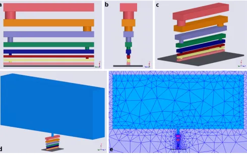
As discussed in the previous section, the EM radiation from a CMOS IC primarily originates from the metal layer routings. To develop a better understanding of the situation, the net radiation can be split into contributions originating from each individual interconnect in the routing. A simple structure that can be used to analyze the radiation properties of different metal layers is a vertical stack of interconnects, joined by vias. We have chosen the dimensions of the interconnects in different layers following Intel’s 32 nm technology node as listed in Table I [27]. The cross-section of the targeted struc-ture is shown in Figure 3, and the resulting model is shown in Figure 4. We use Ansoft HFSS, a finite element method (FEM) based EM simulator to solve Maxwells equations in the system. The excitation to the system is provided via a lumped port in HFSS between the bottom-most metal layer and a perfect electric conductor (PEC) plate functioning as a ground. This style of excitation is similar to the feed of a dipole antenna, and is justified due to the similarity of the system to an infinitesimal dipole, as described in the preceding section. The length of each interconnect layer is taken to be
Fig. 4. Modeling the Interconnect Stack for the Intel 32 nm CMOS process: (a) Metal 1-8 side view, (b) cross-sectional view, and (c) isometric projection; (d) isometric projection with metal layer 9 included; (e) adaptive meshing in HFSS.
200 400 600 800 1000
-75 -50 -25 0 25 50 75
Metal 1-9 Metal 1-8 Metal 1-7 Metal 1-6 Metal 1-5 Metal 1-4 Metal 1-3 Metal 1-2 Metal 1
E
F
iel
d
A
mp
li
tu
d
e
(d
B
)
Distance (µm)
a) Far Field Radiation Pattern b) Decay of Electric Field with Distance
Fig. 5. Simulation Results at 1 GHz excitation: Field Pattern. (a) Far-field radiation pattern, (b) E-field amplitude in dB (with reference at 1 V/m) vs distance for varying number of metal layers in the stack.
3µm. A sphere of radius 1 mm (represents close proximity of the attacker to the IC) enclosing the interconnect stack is used as the simulation region to limit the analysis within a finite volume. A radiation boundary is applied at the surface of the spherical region to eliminate reflection of incident radiation from the outer surface of the simulation region.
Electric Field Analysis: Contribution of Metal Layers
This interconnect stack system is excited at 1 GHz and the electric field amplitude is measured with distance from the structure. The far-field radiation pattern, as shown in Figure 5(a), is analogous to that of a dipole antenna [26], as postulated earlier. We repeat the simulation multiple times, eliminating the topmost metal layer in each subsequent run, and examine the decay of radiated electric field with distance for each structure, as shown in Figure 5(b). This allows us to estimate the radiation contribution of each individual metal layer. For example, the difference between the E-field amplitudes obtained for M1−9 and M1−8 provides an
E-800 850 900 950 1000 0.00 0.02 0.04 0.06 E F iel d A mp li tu d e (V /m)
Distance (µm) Metal 1-9 Metal 1-8 Metal 1-7 Metal 1-6 Metal 1-5 Metal 1-4 Metal 1-3 Metal 1-2 Metal 1 M₉
M₁ to M₈
0 100 200 300 400 500 8000 0.000
0.010 0.020 0.030 0.040
Lower level metals (M1 to M8)
M9 E F iel d C o n tr ib u ti o n ( V /m)
Metal Layer Thickness (nm)
D = 900 µm
800 850 900 950 1000
0.000 0.004 0.008 0.012 E F iel d A mp li tu d e (V/ m ) Distance (µm) Metal 1-8 Metal 1-7 Metal 1-6 Metal 1-5 Metal 1-4 Metal 1-3 Metal 1-2 Metal 1 M₈ M₇ M₆ M₅
100 200 300 400 500
0.000 0.001 0.002 M1/2/3 M4 M5 M6 M7 M8 E F iel d C o n tr ib u ti o n ( V/ m)
Metal Layer Thickness (nm)
D = 900 µm
a) b)
c) d)
E-Field Decay with Distance Contribution of Metal Layers
Fig. 6. (a) E-field amplitude for the metal stack (layers 1 through 8) reduces as each layer is eliminated, (b) Contribution of Metal Layers 1 to 8, showing a linear relation with the dimension of the metal layers. (c, d) E-field contributions of the metals 1 through 9.
field in the near-field region, whereas current through loops creates more H-field in the near-field. Hence, for closed loop differential elements in a chip, H-field would be dominant in near-field which can be examined using similar analysis.
IV. E-FIELDLEAKAGE DETECTION FROM THE METAL LAYERS: SIMULATIONRESULTS
To quantify the contribution of each layer at a particular distance from the probe (D), we utilize the simulated field amplitudes for the metal layer combination at D = 900µm
(Figure 6) and compute the difference between adjacent traces. The individual contribution of the layers to the E-field show a strong linear correlation with the dimensions of the metal lay-ers. This is shown in Figure 6(a, b) where E-field contributions ofM1-M8is plotted against the thickness of those layers. The
thickness ofM9increases by a factor of 16 compared toM8,
and this translates into a significant E-field contribution from
M9 alone, as seen from Figure 6(c, d).
Evidently, the radiation from top-level metal layers in a CMOS IC is significantly higher compared to that from the lower levels. It is therefore imperative for an EM SCA countermeasure strategy to minimize the radiation from top-level metal layers, for excitations that originate from the cell-level. In fact, in this specific example of excitation model using the Intel 32 nm interconnect stack, if the radiation contribution from M9 is eliminated, the net radiation at a distance of
900µmdrops below the sensitivity of commercially available E-field probes.
Accordingly, the detectable EM leakage from the metal layers can be formulated in terms of the noise floor (N Foscilloscope) of the oscilloscope, the transfer function of
the radiated electric field (E) to the current (I) flowing through
0 100 200 300 400 500 8000 0.000
0.010 0.020 0.030 0.040
Detection threshold of commercial E-field probes
Lower level metals (M1 to M8) M9 E F iel d C o n tr ib u ti o n ( V /m )
Metal Layer Thickness (nm) D = 900 µm
0.1 1 10 100 1000 10000 -120 -110 -100 -90 -80 -70 -60 -50 -40 -30
-50 dBm @ 1 GHz (E-Field at probe: 1 V/m)
O u tp u t P o w er ( d B m) Frequency (MHz)
a)E-Field Probe Frequency Response b)Detection Threshold of E-Field Probe
Fig. 7. Sensitivity of the commercial EM Probes: (a) Frequency Response of a commercial E-Field probes (Probe 1 [28], Probe 2 [29]), (b) AtD= 900µm, a commercial E-field probe can potentially detect radiation from Metal Layer 9 (Intel 32 nm process).
the interconnects for different metal layers (MX) and the response of the E-field probe (Figure 7), as shown in Eqn. 2. Note that,EI represents the electric field generated due to the AES current.
iAES EI
MX VE
probe≥N Foscilloscope (2)
The total electric field measured by the external probe is the sum of contribution from the AES engine (EIlocal) and the unrelated logic (EIglobal) present in the circuit, as given in Eqn. 3. EIglobal is the electric field from the global chip routing, whereasEIlocal is from the local routing of the AES engine. Hence, typically, the AES engine is a small portion of the whole chip, that is,EIglobal EIlocal.
EI =EIlocal+EIglobal (3)
The E-fieldEI is measurable as long as the output voltage from the E-field probe (depending on theVE transfer function of the probe) is above the noise floor of the oscilloscope (typi-cally,N Foscilloscopeis∼ −90dBmat 1 GHz). Hence, as seen in Figure 7(a, b), the detectable E-field is ∼10mV /metre, which means that E-field leakage from the metals up to the layer 8 in Intel 32 nm technology is not detectable.
It is to be noted that the analysis of the interconnect stack has been performed at 1 GHz where the EM probes have high sensitivity (Figure 7(a)), and hence encryption engines running at lower clock frequencies will have less detectable leakage as the probe sensitivity reduces at lower frequencies. Also, depending on the technology process, different metal layers may radiate above the detectable threshold. Based on these observations, we proposeSTELLARaround the crypto IP with local low-level metal routing, which attenuates the signature before it reaches the higher metal layers, and thus provides EM SCA immunity as discussed in the subsequent sections.
V. STELLAR: A LOWOVERHEADGENERIC
COUNTERMEASURE AGAINSTEM SCA
AES-128
Signature Attenuation
Hardware Noise Injection
(optional)
Supply Pin
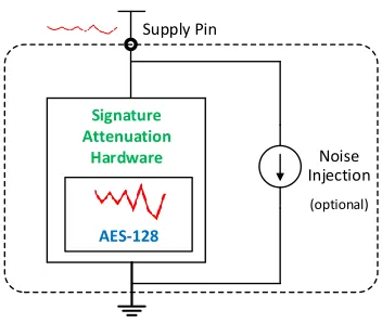
Fig. 8. Overview of the Attenuated Signature Noise Injection (ASNI) AES [15]. Note that the additional noise injection is not necessary if the attenuated crypto signature is lower than the pre-existing noise in the sytem, which arises from the uncorrelated switching currents from other circuit blocks and the input referred noise of the measurement system.
against EM SCA. Hence, our goal is to protect those higher metal layers from leaking sensitive information during the AES encryption operation.
In this regard, if we can somehow completely “shield” the top metal layer (M9for our example with Intel 32nm process)
by suppressing the encryption signature even before it reaches
M9, then there would be no detectable EM leakage from
the encryption IC. Thus, solving the EM SCA problem is reduced to solving the power SCA problem in the lower-level metal layers, that is, suppressing the AES signature completely before it reaches the top-level metal layers. Keeping this in mind, we revisit the existing power SCA countermeasures.
Power SCA countermeasures include power balancing, hardware masking, noise injection, and supply isolation. Power balancing logic implementations involve sense-amplifier based logic (SABL) [30], dual-rail circuits [31], and wave dynamic differential logic (WDDL) [32].
Algorithmic masking is a logic-level countermeasure that involves replacing each logic operation with a sophisticated one to obfuscate the power consumption, leading to high power and area overheads (>4×) [23], [33].
Physical countermeasures include noise injection, switched capacitors, integrated voltage regulators (IVRs), and attenuated signature noise injection (ASNI). Noise injection alone incurs very high power overheads (> 15× to achieve MTD of 50K) [13], [24] and is not an optimum solution. The switched capacitor current equalizer module proposed by Tokunaga et al. [34] is a novel technique against power SCA, however it re-sulted in a2×performance degradation in addition to the33% power overhead. IVR-based implementations utilize traditional low-dropout regulators (LDOs) [35] and buck converters [36]. However, IVRs require large passives and thus consume>2×
power and area overheads, and use the bondwire inductances, which can leak critical information in the form of EM em-anations. Hence, this IVR-based countermeasure cannot be directly used for protecting against EM SCA.
Recently, Attenuated Signature Noise Injection (ASNI) has
IAES CLoad Digital Control Loop Supply Pin
Current Source
Vreg
Vtarget Vtarget+Δ+ Vtarget-Δ
-INoise (optional)
IAES Supply Pin
Vreg Current Source
CLoad
a)
b)
Bleed Shunt LDO
Fig. 9. Background Work: Build-up to the SAH: (a) An ideal implementation, (b) ASNI-AES architecture with Signature Attenuation and Noise Injection to defend against power side-channel attacks [15].
been proposed as a low-overhead generic countermeasure against power SCA [15]. It embeds the AES engine in a Sig-nature Attenuating Hardware (SAH) which highly suppresses the variations in the AES signature with significantly low overhead. As the AES signature gets attenuated by>200×, a very small noise injection can decorrelate the power traces so that the traces obtained by probing at the observable power pin of the encryption ASIC are independent of the AES transitions (M T D >1M). ASNI reduces the signal-to-noise ratio (SNR), both by strongly suppressing the signature, followed by tiny noise injection. However, ASNI is a power SCA countermeasure and does not constrain the placement or routing within the IC.
A. Background: Attenuated Signature Noise Injection (ASNI)
Figure 8 shows an overview of the ASNI circuit. The underlying idea of ASNI is to embed the encryption engine (AES) in a signature attenuating hardware (SAH), such that the variations in the AES current is highly suppressed and is not reflected in the supply current traces, thereby requiring significantly lower noise current injection to decorrelate the measured supply traces [15].
ASNI uses SAH to attenuate (attenuation factor = AF) the AES signature so that the supply current (ICS) becomes highly independent (high attenuation: AF → 0) of the AES signal transitions. Here, it should be noted that the MTD is inversely proportional to the signal-to-noise ratio (SNR), as seen from Eqns. 4, 5 [37], [38], wherek1is the success-rate dependent
co-efficient, andAT = AF1 represents the attenuation due to the SAH.
M T D=k1∗
1
ρ2 T H
≈k1∗(1 +
1
SN R) (4)
SN R= σ
2 T0
σ2 N oise
= σ
2
T/AT
2
σ2
Nexisting+σ 2
Nadd(optional)
(5)
It is to be noted that the additional noise (Nadd) is not
to the uncorrelated switching from other circuit blocks and the input referred noise of the measurement system.
The build-up to the SAH is shown in Figure 9. Figure 9(a) shows an ideal implementation involving an ideal constant current source on top of the AES engine, with an integrating load capacitor (CLoad) to account for the differences in the constant supply current and the variable AES current. This ideal topology only works if the constant current source supplies the average AES currentiAESavgover time. However, practically it is not feasible since ifICS> iAESavg, the output
voltage (Vreg) approaches VDD (supply voltage) with time, due to the integration effects of the load capacitor, without any voltage regulation. Again, when ICS < iAESavg, the
output voltage (Vreg) approaches 0V with time, without any
regulation. Hence, the constraint that the supply current needs to be set to the average AES current is not practical and leads to a meta-stable state of operation without ensuring proper regulation of the output voltage, leading to a performance hit. Hence, as shown in Figure 9(b), a shunt low-dropout (LDO) regulator loop with a bleed device (NMOS) is used to dissipate the overhead residual current (Ibleed) and thus acts as a correction mechanism to compensate for the integration effects of the load capacitor, as shown in Figure 9. This topology called the shunt LDO-based control loop senses
Vreg and controls the bleed NMOS gate voltage to draw the difference of current betweenICSandIAES. Thus, this circuit is able to simultaneously regulate Vreg while keeping ICS
independent of IAES, thereby providing a significant time-variant attenuation by switching between small-signal and large-signal domains.
Another switched-mode control (SMC) digital loop tracks the large changes in the average AES currents and com-pensates for any process, temperature or voltage variations. However, once the supply current is set, the SMC digital loop is disengaged (grayed out in Figure 9(b)) in the steady-state operation of the SAH.
B. Proposed STELLAR Technique
We propose STELLAR: Signature aTtenuation
Embed-ded CRYPTO with Low-Level metAl Routing, which
uti-lizes a Signature Attenuating Hardware (SAH), such as the ASNI circuit, with local low-level metal routing around the crypto IP and suppresses the critical signature before reaching the topmost metal layers which radiate significantly.
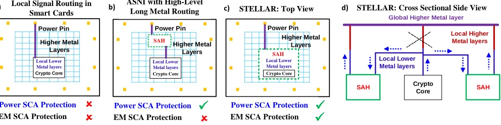
Figure 10 shows the proposedSTELLARhardware with the crypto IP routed within the local low-level metal layers 1 through 7, which then connects to the global higher metal layer 9 (whose leakage is detectable by commercial probes) through the SAH in the form of ASNI. Hence, STELLAR locally embeds the AES-128 core with low-level routing, suppresses the signature through ASNI and routes the attenuated signature through to the global higher metal layers, which is finally connected to the metal pads, as illustrated in Figure 11(a).
Figure 11(a) shows the routing strategy in a smart card, where the crypto signals are routed within the lower metal layers. However, these signals have to come through the
Crypto IP SAH
Cell-level Routing Intermediate Layers: Global Interconnects
Top Layers:
, GND, Clk
Full Encryption Signature
Crypto IP may include all the encryption
algorithms: AES-128, SHA-3, ECC. Generic Countermeasure
Direction of current flow
Global High-level Metal
Local High-level Metal
Local Low-level Metals
EM Leakage not detectable by
state-of-the-art EM probes
Attenuated Signature
STELLAR: Signature aTtenuation Embedded CRYPTO with Low-Level metAL Routing
Fig. 10. Proposed Stellar Technique with local SAH around the crypto block with low-level metal routing for EM Side-Channel Attack Protection.
external pins to connect to the supply, and those power routing is done through the higher metal layers, which is the root-cause of the EM leakage as we studied in Section 3, 4. Hence, only local signal routing does not prevent EM leakage, and hence a signature attenuation hardware (SAH) is necessary.
Figure 11(b) shows that the ASNI circuit with high-level long metal routing with the crypto block although attenuates the current signature from reaching the power pin using the SAH, but does not prevent EM side-channel leakage.
Hence, we proposeSTELLAR(Figure 11(c)), which utilizes the SAH locally around the crypto block with low-level metal routing and attenuates the current signature within the lower metal layers, and thus prevents any detectable EM leakage from the higher metal layers (carrying the attenuated power signatures) which connects to the external pins.
The cross-sectional block-level layout of the STELLAR (Figure 11(d)) shows the current flow through the metal layers connecting the crypto core and the SAH with the metal layers. The crypto core locally embedded within the SAH is routed using the local lower metal layers, which in turn connects directly to the global higher metal layers.
STELLAR uses the SAH which provides high attenuation (1/AF) and the attenuation factor (AF) depends on the choices of the load capacitor (CLoad), amount of overhead bleed
SAH
Crypto Core
SAH
Global Higher Metal layer
Local Higher Metal layers
Local Lower Metal layers
Crypto Core
Local Lower Metal layers
SAH
Crypto Core Local Lower Metal layers
Crypto Core
SAH
Local Lower Metal layers
STELLAR: Cross Sectional Side View
d) a) Local Signal Routing in
Smart Cards
Higher Metal Layers Power Pin
Power SCA Protection EM SCA Protection
ASNI with High-Level Long Metal Routing
b)
Higher Metal Layers Power Pin
Power SCA Protection EM SCA Protection
STELLAR: Top View
Higher Metal Layers Power Pin
c)
Power SCA Protection EM SCA Protection
Fig. 11. (a) Low-level metal layer Signal Routing traditionally used in smart-cards does not reduce EM leakage as the signals have to come through the higher level metals to connect to the external pin, (b) ASNI with high-level long metal routing prevents power SCA, but not EM SCA, (c) STELLAR technique utilizing the SAH block around the crypto IP locally routed with low-level metal layers and the attenuated signature flows through the leaky high-level metals, (d) Cross-sectional side-view of the STELLAR shows that the higher metal layers are isolated from the crypto core, thus carrying a highly suppressed encryption signature after being passed through the SAH (ASNI) circuit.
Fig. 12. Snapshot of the time-domain waveforms of the signature Attenuation hardware utilized by the STELLAR-AES.
in the case of STELLAR-AES is quantitatively analyzed in Section VI.A.
VI. STELLAR: LOCALASNIAROUNDCRYPTO-IPWITH LOWER METAL ROUTING
In the previous section, we have investigated the power SCA countermeasures and proposed the STELLAR technique utilizing the ASNI circuit to provide significant attenuation to the AES signature with extremely low overheads. In Section 4, we have also analyzed that the EM emanations from metal 9 is detectable using commercial EM probes for the Intel 32 nm CMOS process. However, the threshold may vary depending on the particular CMOS process, as discussed earlier. Hence, if we “shield” the high-level metal layers (M9in this case) by
encapsulating the locally-routed AES engine with the ASNI hardware (Figure 10, 11), then the AES signature cannot be detected by an external EM attacker. Hence, we now evaluate the STELLAR hardware placed on top of the AES-128 core designed in TSMC 65 nm CMOS process 1.
In STELLAR, the placement of the AES core encapsulated by the ASNI circuit is very critical and has security, power and performance trade-offs. To achieve the highest level of
1Note that, due to NDA reasons, we do not provide the metal stack
information for TSMC 65 nm technology, in which the STELLAR design and simulations are carried out. The EM analysis is performed on the Intel 32nm process as the interconnect stack dimensions are publicly available [25].
security against EM SCA (maximum MTD), the ASNI along with the AES needs to be routed with the lowest metal layers. Although it provides maximum signature suppression (leading to the minimum noise injection overhead), lower metal layers suffer from high resistance and may result in a high voltage drop across the output voltage (Vreg), which can degrade performance (leading to lower throughput) of the AES encryption engine. The AES-128 core design consumes a physical chip area of ∼0.35mm2 [15]. Assuming that the maximum length of routing isLmax= 350µm∗
√
2 = 493µm
and we can tolerate an output voltage drop of 10mV, the maximum tolerable routing resistance (Rmax) is given by
Eqn. 6.
Rmax= ∆Vmax
iAESavg
= 10mV
1mA = 10Ω. (6)
RLmax= Rmax
Lmax =
10Ω
493µm ≈0.02Ω/µm (7)
Hence, we can route the STELLAR-AES core only with metal layers for which R < RLmax = 0.02Ω/µm(Eqn. 7). Now, considering the Intel 32 nm CMOS process, only metals above layer 7 provides the desired low routing resistances and hence has no performance degradation in the operation of the cryptographic core. Thus, the AES can be routed up to metal layer 7 (as shown in Figure 10) and shielded with the ASNI hardware so that signals leaking to higher metal layers (M8, M9) are highly attenuated. However, the placement of the
ASNI-AES core needs to be analyzed in design-time depend-ing on the particular process (CMOS technology). STELLAR using the local ASNI provides an attenuation (AF1 ) to the AES signature such that the measured electric field (Eqns. 2, 3) gets modified accordingly as shown in Eqns. 8, 9, 10.
EIST ELLAR= EIlocal
ATlocal +
EIglobal
Correct Key Incorrect Keys
CEMA on the STELLAR-AES with different levels of noise injection CEMA on the
Baseline AES-128
a) b) c)
Correct Key Incorrect Keys Correct Key
Incorrect Keys
MTD
MTD
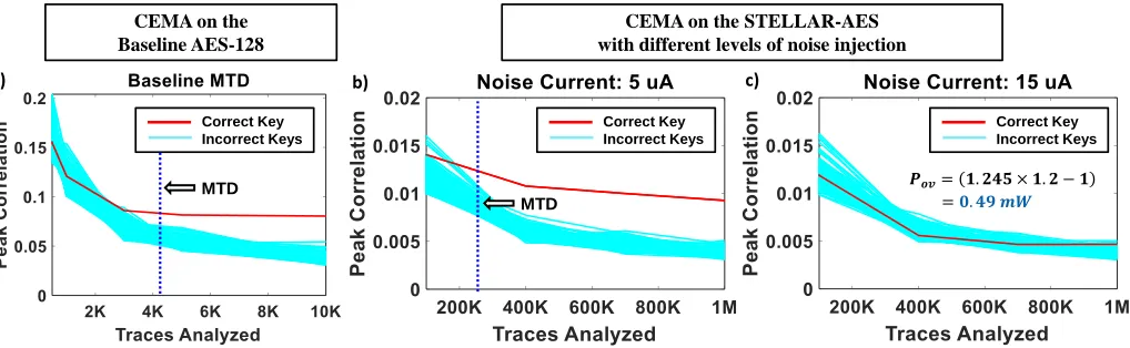
Fig. 13. MTD Analysis: (a) Minimum Traces to Disclosure (MTD) for a CEMA attack on the baseline AES-128 implementation, (b, c) Locally-routed STELLAR-AES: Noise Injection on the modified AES in Attenuated Signature domain, to achieve MTD of 1 Million traces.
ATlocal= M9 MXCrypto
: E-field reduction due to absence
of higher local metal layers (9)
ATglobal=
1
AFSAH
:AES Signature Suppression using SAH (10)
Hence, as seen from Eqns. 9, 10, the overall SNR reduc-tion has two key components: (1) Electric field suppression (ATlocal) achieved due to the absence of routing through the local high-level metal layers (M8in our case, refer Figure 10).
In this case, if the AES-128 core embedded within the SAH (ASNI) block is routed with local low-level metal M1 toM7
(meeting the constraint presented in Eqn. 6, 7), the ASNI hardware can then directly connect to the global high-level metal M9, and thus ATlocal = MM97 ≈ 20 (from Table 1).
(2) AES Signature suppression (ATglobal) using SAH ensures
that although the EM signal leakage from the global metal layers remain the same, the correlated signature present in the emanated E-field is significantly attenuated.
Now, the ratio of the electric fields contributed by the local and global routing from the AES block can be attributed to the relative area of the AES to the area of the rest of the circuit (refer Figure 11 (a) - the higher metals form a mesh structure throughout), as given in Eqn. 11,
EIlocal EIglobal =
Area of AES
Total Chip Area - Area of AES - Area of pads
≈ 200µ×200µ
1m×1m−200µ×200µ =
1
24. (11)
Now, from Eqn. 3 and Figure 6(a), we see that for an excitation of 1V with 50 Ω termination (i = 20mA),
EIlocal+EIglobal = 35mV /mat a probe distance of900µm. This translates to an electric field of EI ≈6mV /m for our
case with an AES peak current iAESmax = 3.2mA. Using
Eqn. 11, we obtain EIlocal = 1
24 ∗6 = 0.25mV /m and EIglobal =
23
24∗6 = 5.75mV /m.
As the STELLAR hardware is embedded on top of the AES-128 encryption engine, using Eqns. 8, 9, 10 the measured electric field becomes EIST ELLAR = 020.25+5200.75 ≈ 0.04mV /m, which means that the effective suppression of the AES signature is ∼150×.
A. Results & Overhead Comparison
We perform CEMA attack on the AES-128 core (1st round S-Box operation) with a clock frequency of 40 MHz and an average current (IAESavg) of ∼ 1mA (peak current = 3.2
mA). The AES-128 engine performs one block encryption in 10 cycles. The CEMA attack reveals the secret key of the unprotected AES within<6K traces (Figure 13(a)), whereas the same attack on the STELLAR-AES does not reveal the secret key even with1M traces (Figure 13(c)).
Figure 13(b, c) shows the evolution of the MTD with differ-ent levels of noise injection after the signature attenuation of the locally routed AES engine (STELLAR-AES). Figure 13(c) shows that only15µAof noise current injection is required to achieve Minimum Traces to Disclosure (MTD)>1M.
Using Eqns. 4, 5, the relation between MTD, ASNI sig-nature attenuation factor (AFASN I) and the overall noise
(IN oise, includes the pre-existing system noise) is given by
Eqn. 12.
M T D∝ 1
SN R ∝(AT ∗IN oise)
2∝
IN oise AFASN I
2
(12)
Hence, for a higher MTD, more noise may be injected or the attenuation (AT) may be enhanced, which could be achieved by the lower-level routing (increasingATlocal), or by increasing the ASNI circuit attenuation (ATglobal =AF1
ASN I).
With the same level of attenuation, the amount of noise current required to achieve MTD of 100M would beIN oise∼
15µA∗q100M
1M = 150µA.
The current consumed by the amplifier in the shunt LDO loop consumes a current of ∼ 100µA and hence the total overhead current is given asIov=Ibleed+Inoise+Iopamp=
M T D > 1M the total overhead power for the STELLAR-AES architecture is(1.13mA+ 0.015mA+ 0.1mA)∗1.2V− 1mA∗1V = 0.49mW. Power efficiency for STELLAR-AES is given as, η = (1.245(1mAmA∗1∗V1.)2V) ∗ 100 ≈ 67% (includes noise overhead). Hence, STELLAR-AES consumes similar overhead as [18], but does not incur the performance penalty. Implementation of the SAH consumes an area of∼0.08mm2,
while a standalone AES incurs 0.35mm2, which implies an
area overhead of ∼22.85%, for M T D >1M.
VII. CONCLUSION
Electromagnetic emission from cryptographic ICs is a prominent side-channel attack vector to extract the secret key without physical access to the device. The growth of internet-connected small form-factor devices and the availability of cheap commercial EM probes calls for an efficient coun-termeasure against EM SCA. This paper, for the first time, performs a white-box modeling of the interconnect metal-via stack within an integrated circuit which leaks critical signal transitions in the form of EM radiation. System-level modeling of the interconnect structure for Intel 32 nm CMOS process reveals that metals above layer 8 leak the most and can be detectable using commercially available cheap EM probes. This work proposes the STELLAR technique to locally route the AES-128 encryption engine in the lower-level metal layers and also encapsulated within a low-overhead signature suppression hardware (ASNI). The ASNI circuit is then routed to the leaky higher-level metals, which now contains only the suppressed AES signatures. Hence, using STELLAR with local low-level metal routing along with the SAH as an efficient“shield” protects the AES-128 encryption signatures from radiating, thereby achieving M T D > 1M with only a tiny noise injection of 15µA. STELLAR with low-level metal routing with the SAH (ASNI) local encapsulation around the crypto block not only provides a low-overhead solution (1.5×
power, 1.23× area overhead) against EM SCA, but it is also a generic countermeasure and can be extended to other cryptographic engines.
REFERENCES
[1] P. Kocher et al., “Differential Power Analysis,” inAdvances in Cryptol-ogy CRYPTO 99, ser. Lecture Notes in Computer Science, M. Wiener, Ed. Springer Berlin Heidelberg, Aug. 1999, no. 1666, pp. 388–397. [2] E. Brier et al., “Correlation Power Analysis with a Leakage Model,” in
CHES, Aug. 2004, no. 3156, pp. 16–29.
[3] K. Gandolfi et al., “Electromagnetic Analysis: Concrete Results,” in CHES. Springer, Berlin, Heidelberg, May 2001, pp. 251–261. [4] J.-J. Quisquater and D. Samyde, “ElectroMagnetic Analysis (EMA):
Measures and Counter-measures for Smart Cards,” in Smart Card Programming and Security. Springer, 2001, pp. 200–210.
[5] D. Genkin et al., “RSA Key Extraction via Low-Bandwidth Acoustic Cryptanalysis,” inCRYPTO, Aug. 2014, pp. 444–461.
[6] D. Brumley et al., “Remote Timing Attacks Are Practical,” in Usenix Security Symposium, Berkeley, 2003, pp. 1–1.
[7] D. Genkin et al., “Stealing Keys from PCs Using a Radio: Cheap Electromagnetic Attacks on Windowed Exponentiation,” inCHES 2015. Springer, Berlin, Heidelberg, Sep. 2015, pp. 207–228.
[8] Genkin et al., Daniel, “ECDH Key-Extraction via Low-Bandwidth Electromagnetic Attacks on PCs,” Tech. Rep. 129, 2016.
[9] E. D. Mulder et al., “Electromagnetic Analysis Attack on an FPGA Implementation of an Elliptic Curve Cryptosystem,” in EUROCON 2005, vol. 2, Nov. 2005, pp. 1879–1882.
[10] T.-H. Le et al., “A Proposition for Correlation Power Analysis Enhance-ment,” inCHES, Oct. 2006, pp. 174–186.
[11] C. O’Flynn, “A Framework for Embedded Hardware Security Analysis,” Jul. 2017.
[12] S. Mangard et al.,Power Analysis Attacks: Revealing the Secrets of Smart Cards. Springer US, 2007.
[13] T. Guneysu and A. Moradi, “Generic Side-Channel Countermeasures for Reconfigurable Devices,” inCHES 2011, Sep. 2011, pp. 33–48. [14] E. Peeters et al., “Power and electromagnetic analysis: Improved model,
consequences and comparisons,”Integration, the VLSI Journal, vol. 40, no. 1, pp. 52–60, Jan. 2007.
[15] D. Das et al., “ASNI: Attenuated Signature Noise Injection for Low-Overhead Power Side-Channel Attack Immunity,”IEEE Transactions on Circuits and Systems I: Regular Papers, pp. 1–12, 2018.
[16] C. O’Flynn and C. Zhizhang, “ChipWhisperer: An Open-Source Plat-form for Hardware Embedded Security Research,” 2014.
[17] D. Agrawal et al., “The EM SideChannel(s),” inCHES, Aug. 2002, pp. 29–45.
[18] T. Ordas et al., “Near-Field Mapping System to Scan in Time Domain the Magnetic Emissions of Integrated Circuits,” Sep. 2008, pp. 229–236. [19] V. Lomne et al., “Evaluation on FPGA of Triple Rail Logic Robustness
Against DPA and DEMA,” ser. DATE, 2009, pp. 634–639.
[20] A. Kumar et al., “Efficient simulation of EM side-channel attack resilience,” inICCAD, Nov. 2017, pp. 123–130.
[21] N. Homma et al., “EM Attack Is Non-invasive? - Design Methodology and Validity Verification of EM Attack Sensor,” inCHES, Sep. 2014, pp. 1–16.
[22] M. Yamaguchi et al., “Development of an on-chip micro shielded-loop probe to evaluate performance of magnetic film to protect a crypto-graphic LSI from electromagnetic analysis,” in2010 IEEE International Symposium on Electromagnetic Compatibility, Jul. 2010, pp. 103–108. [23] O. Reparaz et al., “Consolidating Masking Schemes,” inCRYPTO, ser.
Lecture Notes in Computer Science, Aug. 2015, pp. 764–783. [24] D. Das et al., “High efficiency power side-channel attack immunity using
noise injection in attenuated signature domain,” in IEEE HOST, May 2017, pp. 62–67.
[25] S. Natarajan et al., “A 32nm logic technology featuring 2nd-generation high-k + metal-gate transistors, enhanced channel strain and 0.171 um2 SRAM cell size in a 291mb array,” in2008 IEEE International Electron Devices Meeting, Dec. 2008, pp. 1–3.
[26] C. A. Balanis,Antenna Theory: Analysis and Design, 4th ed. Hoboken, NJ: Wiley, Feb. 2016.
[27] P. Packan et al., “High performance 32nm logic technology featuring 2nd generation high-k + metal gate transistors.” IEEE IEDM, Dec. 2009, pp. 1–4.
[28] T. D. Solutions, “Tekbox EMC Near-field Probes Manual.” [29] A. EM Probe Manual, “RF Near Field Probe Set DC to 9ghz.” [30] K. Tiri et al., “A dynamic and differential CMOS logic with signal
independent power consumption to withstand differential power analysis on smart cards,” in Proceedings of the 28th European Solid-State Circuits Conference, Sep. 2002, pp. 403–406.
[31] M. Bucci et al., “Three-Phase Dual-Rail Pre-charge Logic,” inCHES, ser. Lecture Notes in Computer Science, Oct. 2006, pp. 232–241. [32] D. D. Hwang et al., “AES-Based Security Coprocessor IC in 0.18-um
CMOS With Resistance to Differential Power Analysis Side-Channel Attacks,”IEEE JSSC, vol. 41, no. 4, pp. 781–792, Apr. 2006. [33] T. D. Cnudde et al., “Hardware Masking, Revisited,”IACR Transactions
on Cryptographic Hardware and Embedded Systems, vol. 2018, no. 2, pp. 123–148, May 2018.
[34] C. Tokunaga and D. Blaauw, “Securing Encryption Systems With a Switched Capacitor Current Equalizer,” IEEE Journal of Solid-State Circuits, vol. 45, no. 1, pp. 23–31, Jan. 2010.
[35] A. Singh et al., “Integrated all-digital low-dropout regulator as a coun-termeasure to power attack in encryption engines,” inIEEE HOST, May 2016, pp. 145–148.
[36] M. Kar et al., “8.1 Improved power-side-channel-attack resistance of an AES-128 core via a security-aware integrated buck voltage regulator,” inISSCC, Feb. 2017, pp. 142–143.
[37] S. Mangard, “Hardware Countermeasures against DPA A Statistical Analysis of Their Effectiveness,” inTopics in Cryptology CT-RSA 2004. Springer, Berlin, Heidelberg, Feb. 2004, pp. 222–235.
![Fig. 3. Cross-Section of the Interconnect Stack (Intel 32 nm) [25], (a) Metal1 through 8 (b) Includes metal 9 and the copper bump layer.](https://thumb-us.123doks.com/thumbv2/123dok_us/7979039.1323277/3.612.369.505.204.314/cross-section-interconnect-stack-intel-metal-includes-copper.webp)
![Fig. 7. Sensitivity of the commercial EM Probes: (a) Frequency Response of acommercial E-Field probes (Probe 1 [28], Probe 2 [29]), (b) At D = 900µm,a commercial E-field probe can potentially detect radiation from Metal Layer9 (Intel 32 nm process).](https://thumb-us.123doks.com/thumbv2/123dok_us/7979039.1323277/5.612.49.302.53.265/sensitivity-commercial-frequency-response-acommercial-commercial-potentially-radiation.webp)