510
Review article on Quantum Dots: Synthesis, Properties
and Application
P.V. Joglekar
1, D.J.Mandalkar
2, M.A. Nikam
3, N.S. Pande
4, A. Dubal
5School of Engineering1,2,3,4,5,Symbiosis Skills and Open University, Kiwale, Pune, India1,2,3,4,5 Email: [email protected] 1, [email protected] 2
Abstract- Quantum dots also known as quasi zero dimensional system are nanostructures with a wide range of engineering applications. This manuscript reviews various synthesis routes of Quantum Dots. Of the various methods, chemical synthesis, chemical vapour deposition-gas phase synthesis, laser ablation, molecular beam epitaxial, lithographic methods have been discussed and overviewed. The latter half of the paper discusses some properties and applications of quantum dots. Their interesting and unique optical properties, some Quantum Dots also exhibit semi conducting properties results in potential applications in electronics, biology and energy applications.
Index Terms-Quantum dots, planer quantum dots, vertical quantum dots, self-assembled quantum dots, QD colloidal synthesis, QD laser, electroluminescence application, nanotechnology, nanophysics, nanoscience, CdSe, ZnS, chemical vapor deposition.
1. INTRODUCTION
Quantum dots (QD‘s) are nanostructures which confine electrons to zero dimensions. These can be thought of as a 3 D quantum well constrained to zero dimensions. QD‘s are structurally and electrostatically isolated from the outside. In general, they contain few hundreds to millions of atoms but less than hundreds of free electrons [1, 3]. Because of their similarity with atoms they are also referred as artificial atoms [2]. QD‘s which are semi conducting in nature are widely used in various applications. In general, they are composed of elements group II-VI or III-V. Because of the spatial confinement their energy levels become discreet, unlike as continuous energy range levels as in bulk materials. QDs when excited to higher energy levels relax radiatively by emitting a characteristic photon and come to the ground state energy.
2. QUANTUM CONFINEMENT
The electrons in quantum dots have a range of energies. A pair of electron and a hole is called excitons, there is an average physical separation between the electron and hole, which is referred as the Exciton Bohr Radius. Exciton Bohr radius varies from material to material. The Exciton Bohr Radius of a material is extended/ stretched to its natural limit in bulk, as the dimensions of the semiconductor crystal are much larger than the Exciton Bohr Radius. When the size of semiconducting crystal becomes small, comparable to the size of Exciton Bohr radius, then the electron energy levels can no longer be treated as continuous - they must be treated as discrete, as there is a small and finite separation between energy levels. This situation of discrete energy levels is called quantum confinement, and under these conditions, the semiconductor material ceases to resemble bulk, and
instead can be called a quantum dot. This property has influence on the absorptive and emissive behaviour of the semiconductor material [6].
On the basis of type of electron confinement, QDs can be classified into planar QDs, Vertical QDs and self-assembled QDs.
2.1. Planar Quantum Dots
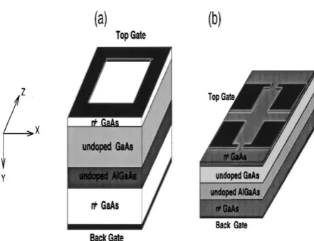
511 Fig. 1. Schematic diagram of planer QD device with
layer structure (a) square (b) quad-gate structure. ref [3].
2.2.Vertical Quantum Dots
A narrow pillar of zero dimensions is vertically sandwiched between heterostructure layers. A disk of GaAs is sandwiched between two thin AlGaAs barriers. Gate electrode surrounding the pillars is negatively biased; this depletes electrons in the outer region of the pillar and shrinks the quantum disk. As a result the electrons are confined at a very narrow region in the center of the pillar. Because of large band gap material, the tunnelling barriers are high; this makes Vertical QDs less sensitive to external fluctuations. The flow of current is vertical, perpendicular to 2DEG.
Inversion channel of conventional MOSFET is replaced by quantum dot. Hence, the most popular application of planar and vertical quantum dots is the single electron transistor.
2.3.Self-Assembled Quantum Dots
The lattice mismatch between two materials for example few monolayers of InAs on GaAs substrate, induces stain leading to breakdown of 2D layered structure resulting randomly distribution of ―self-crystallized islands‖ called self-assembled quantum dots . Typically they have a pyramidal or lens-shaped structure.
3. SYNTHESIS OF QUANTUM DOTS
Quantum dots can be synthesized (broadly) in two ways, Top-Down and Bottom-Up approach. In top-down synthesis, the bulk material is thinned to form quantum dot. The various techniques used in this approach are electron beam lithography, reactive ion etching, focused beam lithography, dip pen lithography. Some of the limitations from this approach are structural imperfections caused by patterning and contamination (addition of impurities) in quantum dots. In the bottom-up approach, various chemical, physical methods are harnessed to form nanoparticles and clusters. Physical methods include
molecular beam epitaxial growth, colloidal synthesis, and physical/ chemical vapor deposition techniques.
3.1.Colloidal Synthesis [8,9]
Preparation of CdSe QDs[8]: Cd(Clo4)2.H20 salt dissolved in water 0.02 M is stirred and thiol stabilizer is added. The pH of soln is controlled by adding NaOH soln. This soln is deaerated by N2 bubbling for 30 mins Solid Bulk Al2Te3 is reacted with dilute sulphuric acid to generate H2Te gas. This gas along with slowly regulated nitrogen is introduced in the solution Cd-RSH precursor. After the exhaustion of H2Te gas the solution is cooled in condenser to get quantum dot. The solution is further heated to form QD nanocrystals. The reactions are as follows:
Cd2+ + H2Te→( HS-R) →Cd-(SR)xTey+2H+
Cd2+ + NaHTe→( HS-R) → Cd-(SR)xTe + H++ Na+
Cd-(SR)xTey →(100˚C) CdTe Quantum Dots
Al2Te3 + H2SO4 →Al2(SO4)3 + 3H2Te(gas)
InAs nanocrystal quantum dots were synthesized using reaction of InCl3 and As[Si(CH3)3]3 [9]. The discreet particles ranging 25-60 ˚Α with a zinc blend structure obtained. The reactants are reacted at high temperatures 240-260 ˚C with triocytlphosphine as a solvent and capping agent to form InAs nanocrystals. Triocytlphosphine makes these QDs soluble in most of common solvents (toluene/methanol).
3.2.QD Synthesis using deposition techniques
[10, 11]
In chemical vapor deposition techniques the reactants generally react in gaseous phase at high temperatures and are deposited on sample surface.
InGaN self-assembled QDs were grown by MOCVD technique [10]. In this method, Hao et al used low V/III ratio and low growth temperature. 30 nm GaN layer was grown on sapphire substrate at 500‘c. A buffer layer was grown on top of it at 1110‘c under H2 ambient gas. GaN layer was formed by reaction of trimethylgallium (TMG-group III source) and NH3 (group V source) ratio of the concentration was 2000. After the buffer layer is grown the temperature is reduced to 660‘c to grow an InGaN (quantum dot/wells) layer using trimethylindium under N2 ambient gas.
512 and simultaneously CdSe nanocrystal QDs grown
ex-situ are dissolved in solvent and electrosprayed in the chamber over the matrix. Hydrogen selenide and Diethylzinc (DEZn) carried in hydrogen gas were used as precursors in CVD to form ZnSe matrix. CdSe-ZnSe nanocrystral growth is controlled using trioctylphosphine-trioctylphosphine oxide (TOP/TOPO). Dimethylcadmium and selenium powder are co-dissolved in a tri-alkyl phosphine (-butyl or -octyl), and the solution injected into hot (340–360 °C), high purity (90% purity) trioctyl phosphine oxide (TOPO). Nucleation occurs rapidly, followed by growth (280–300 °C). The nanocrystals were purified by precipitation with methanol and redispersing with hexane. They are separated using centrifuge. The nanocrystals are electrospray atomized and deposited on matrix. The reactor pressure was maintained at 600 torr.
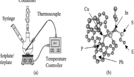
Another typical synthesis example of CdSe QDs by organometallic chemical bath [16, 17] route. In this method trioctylphosphine oxide (TOPO) is heated under an inert atmosphere to between 300 and 350˚C. A mixture of the desired organometallic precursors (eg. phosphine chalconide) is diluted in trioctylphosphine (TOP) and drawn into a syringe. The contents of the syringe are injected into the hot TOPO with vigorous stirring (Fig 7a). The temperature of the bath will decrease, due to the injection of the cooler precursor. The original temperature of the bath is referred to as the injection temperature, and the temperature of the bath as the nucleation occurs is referred as growth temperature. The solutions turns to yellow then to orange and red/brown from colourless in the beginning, as QD size increases. Size is monitored using UV-VIS spectroscopy. Heating is stopped as the desired size is reached. After cooling, excess reagents are removed by adding methanol giving a powdered TOPO-capped nanocrystals. By varying injection temperature, growth temperature and growth time various (with different characteristic) QDs can be synthesized.
Fig. 2. a) Apparatus for quantum dot chemical bath synthesis; (b) single-source CuInS2 molecule. ref [16].
3.3.Gas Phase Synthesis of quantum dots
[18-19]
The gas phase method offers an economical way for synthesizing QDs. The vapor (gas) phase synthesis is a continuous process and offers high purity relative to liquid or solid state processes. Many multi component materials can be synthesized using this process though agglomeration is an issue (drawback) in the process. Deppert et al., [18] used aerosol method to synthesize GaAs (III-V). They used gallium and Arsine (AsH3) as precursors. Ultrafine particles were created (sprayed) using aerosol generator. The particle size selection was done using differential mobility analyser, which is based on principle of electrical mobility of particles is decreases with the size of particle. Aerosol flow is regulated before/as it enters the reaction chamber to form nanocrystals.
Gas phase synthesis can be done in various ways besides above mentioned aerosol way namely, using plasma reactors, laser reactors, flame reactors, inert gas reactors(evaporating and condensing)- sputtering. In plasma reactors, as the precursors enter reaction chamber with high temperature they decompose into ions and atom. They react in ionic form resulting nanoparticles/crystals/structures. An advantage of plasma reactor is that they have high cooling rate. The same process can be done by using laser instead of plasma, in this method highly localized heating and cooling can be achieved.
3.4.Formation of Quantum Dots using LASER
Ablation Technique
In this method [12], high energetic laser light is focused on metal/crystals to create nanoparticles/crystals. Creating nanoparticles by laser ablation of solids in liquid environment is the simplest method. The ejected species remain suspended in liquid forming a kind of nano-suspension. Anikin et al, used Cu laser to obtain CdS/ ZnSe quantum dots of by ablating CdS / ZnSe crystal in open air under a thin layer of liquid above the surface of semiconductor. They used various liquids medium namely, isobutanol (CH3)2CHCH2OH), diethyleneglycole (HOCH2CH2)2O) (DETG), ethanol CH3CH2OH, water, and dimethylsulphoxide (CH3)2SO, (DMSO) without addition of any surface active substances. A suspension of CdS nanocrystals were obtained in various liquid medium.
513 plasma expands in the form of a plume in plane
perpendicular to the target surface. Adiabatic expansion and cooling of the plume leads to the cluster condensation. As the clusters collide with ambient gas molecules they stabilize. The smaller clusters are scattered longer and are deposited at a longer distance from laser spot.
Fig. 3. Schematic diagram showing aerosol generation, sizing and reaction process. ref [18].
3.5. Quantum Dot growth using Molecular Beam Epitaxy (MBE) and nanopatterning.
Wang et al [6] used nano patterned Si (100) substrate to grow patterning assisted Ge quantum dot to get uniform size, placement and high density. Self-assembled diblock copolymer were used to get nanopatterned substrates. Polystyrene-block-poly (methylmethacrylate)(PS-b-PMMA) was used as diblock polymer. Ge quantum dot growth was done by MBE on Si substrate with hexagonally ordered hole patterns on the surface. A 30 nm layer of SiO2 is deposited on wafer using low pressure chemical vapor deposition. Then using spin coating 30 nm layer of PS-b-PMMA is coated on top. PMMS becomes spatially separated from PS after annealing at 170˚C in vacuum. The sample is exposed to ultra violet rays for 35 mins, the PS is cross linked and PMMA is separated. Rinsing is done using acetic acid; cylindrical pores are formed in PS matrix. By dry etching (CHF3), the hexagonally organized cylindrical pattern of PS-b-PMMA on the top layer is transferred to the substrate (SiO2) layer. The hole pattern provide the preferred nucleation site for the Ge dot growth. Growth temperature of 620˚C is maintained for Si layers and 530˚C for Ge layers. The average height of QDs obtained was 5nm, 30nm lateral sizes, and density 1011 cm-2.
4. QUANTUM DOT PROPERTIES AND
APPLICATIONS [6, 14-17]
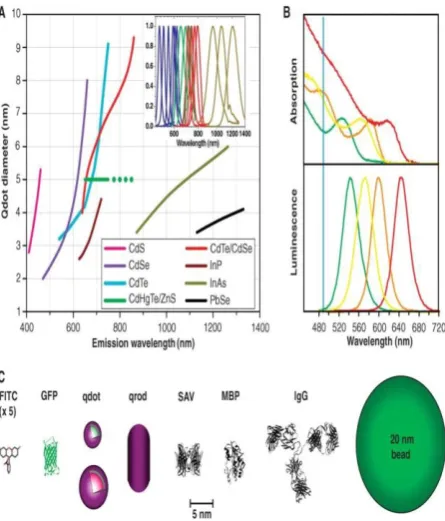
Figure 4 shows (A) emission maxima and sizes of quantum dots of different composition. Quantum dots be synthesized from various types of semiconductor materials (II-VI: CdS, CdSe, CdTe; III-V: InP, InAs; IV-VI: PbSe are characterized by different bulk band gap energies. The curves represent dependence of peak emission wavelength on quantum dot diameter.
The range of emission wavelength is 400 to 1350 nm, with size varying from 2 to 9.5 nm (organic passivation/solubilisation layer not included). All spectra are typically around 30 to 50 nm (full width at half maximum). (B) Absorption (upper curves) and emission (lower curves) spectra of four CdSe/ZnS quantum dot samples. The blue vertical line indicates the 488-nm line of an argon-ion laser, which can be used to efficiently excite all four types of quantum dots simultaneously. (C) Size comparison of quantum dots and comparable objects. FITC, fluorescein isothiocyanate; GFP, green fluorescent protein; quantum dot, green (4 nm, top) and red (6.5 nm, bottom) CdSe/ZnS qds; qrod, rod-shaped quantum dot. Semiconducting quantum dots shows broad absorption spectrum, when a photon is absorbed with energy above the band gap energy this result in creation of exciton (electron-hole pair). At higher energies (shorter wavelengths) the absorption probability is greater resulting in broader spectrum. The long life time and radiative combination of excitons leads to the emission of a photon in a narrow, symmetric energy band. This also enables the use of detection technique called time-gated, which separates the signal from shorter lived species (or background signal).Single quantum dots can be observed for long time and tracked in various microcopies, namely confocal microscopy, total internal reflection microscopy, basic wide- field epifluorescence microscopy. QD‘s large absorption cross section makes them excellent probe for two photon confocal microscopy.
Quantum dot‘s versatile application has leaded itself to be an important candidate in nanotechnology and emergent new technologies. They are used in electronics- single electron transistors, LED‘s, displays, in energy applications as solar cells and photovoltaic. Quantum dots in conjunction with carbon nanotubes are being used in nano-device applications, in single electron transistors. Besides their optical applications, they are also used in life sciences for medical imaging, labeling and sensing. QDs prepared using high temperatures methods are not aqueous soluble, to make them soluble one need to functionalize QD‘s with either hydrophilic functional groups, ligands or by through capping, organic coating. These particles shows characteristics (emit light) in visible and NIR region. Eg. of functionalized QD‘s DNA oligonucleotide or apamer, antibody grafted on QDs, amine or carboxyl group giving cross linking with molecules of thiol group, or using bioconjugation reaction an N-hydroxysuccinimyl ester moiety. Functionalized QDs are used for cell targeting, cell labeling, and drug delivery and in imaging.
514 They were able to observe red, blue, green and white
photoluminescence.
Fig. 4. A) Emission maxima and sizes of quantum dots of different composition. (B) Absorption (upper
curves) and emission (lower curves) spectra of four CdSe/ZnS qdot samples. The blue vertical line indicates the 488-nm line of an argon-ion laser, which is used to excite QDs. (c) Size comparison of QDs and
comparable objects. ref [14].
Raffaelle et al [16] have used QDs in solar cell applications; they have synthesized quantum dots of CdSe, CuInS2, and CuInSe2 for use in an intermediate bandgap solar cell. Typically, semiconductor solar cells have efficiency 33 % (from theoretical model), by the use of quantum dots efficiency can be raised to 60 %. Raffaelle et al., have prepared QDs using typical synthesis route of metal organic chemical vapor deposition. They increase in efficiency is based on following theoretical model which states electronic states in the potential ‗wells‘ are ‗quantized‘ and therefore have discrete energy levels. The overlap of the quantum mechanical states from well-to-well results in mini-band levels that will depend on the width of the wells. This dependence of the energy levels on well width can then be used to ‗tune‘ the device to the solar spectrum. Discrete states as a result of QDs allows for absorption of sub-band gap energies thus increasing the overall solar cell efficiency. Dilute magnetic semiconducting quantum dots are being used spintronics, due to their spin polarization properties [20]. The objective is to control
electron spins, in addition to charges, in order to transmit information and provide new functionality to semiconductor devices. Operational spin-dependent light-emitting diodes (spin LEDs) have been demonstrated that using group II-VI and III-V materials.
QDs have gained a tremendous application in biological area. In the area of bio imaging QDs are being used as a contrast agents in the in-vivo and ex-vivo living cell targeting [14]. As biosensors, QD tagged with antibodies can detect various disease or tumour cells (Streptavidin-QDs were used to detect Her2 cancer markers on the surface of SK-BR-3 human breast cancer cells via a biotinylated secondary antibody to human and a humanized antibody to Her2). Some proteins can be recognized by peptides; hence some peptides are used for QDs functionalization for cell targeting/labelling. QDs have long term stability in-vivo and also due to their brightness they are ideal candidate for live animal targeting and imaging. Two-photon excitation confocal microscopy was used to image blood vessels in live mice that had received QDs by intravenous injection, showing that higher contrast and imaging depth can be obtained at a lower excitation power than with organic dyes. Functionalized QDs as an example of a biotransducer, light-excited QDs could transfer their charge to bound enzymes functioning as electron or hole acceptors, enabling their control by light activation. Reciprocally, QDs could be lit up by electron or hole donor enzymes through chemiluminescence. Quantum dots are promising candidate for wide range of applications and future technologies, some of the proposed applications are defense and anti-counterfeiting by injecting QDs into fabric, liquid mixtures, polymer matrix to produce unique validation signatures.
5. CONCLUSION AND SUMMARY
515
Acknowledgments
The authors would like to thank the Symbiosis Skills and Open University for their encouragement and support.
REFERENCES
[1] S Bandopadhyay, H S Nalwa Eds.,: Quantum Dots and Nanowires, American Scientific Publishing May (2003).
[2] P Matagne, J-P Leburton , Quantum Dots: Artificial Atoms and Molecules, IJMS 2009,10(2), 656-673.
[3] Tamura,Takayanagi ,Shiraishi; Quantum Dot Atoms, Molecules, and Super lattices, American Scientific Publishing (2003).
[4] S Nagaraja et al Shell filling effects and coulomb degeneracy in planar quantum dot structures, Physical Review, Vol 56, No.24 15 Dec 1997-II. [5] S Tarucha et al, Shell Filling and Spin Effects in a
Few Electron Quantum Dot, Phys. Review Letters, vol 77,3613(1996).
[6] K L Wang et al, Ge/Si Self-Assembled Quantum Dots and Their Optoelectronic Device Applications, Proceedings of the IEEE | Vol. 95, No. 9, September 2007.
[7] F Wise, Lead Salt Quantum Dots: the Limit of Strong Quantum Confinement, Acc. Chem. Res. 2000, 33, 773-780.
[8] X Zhang et al, Synthesis of CdTe and PbS semiconductor quantum dots and their biological and photochemical application, UTA, MS Thesis 2010.
[9] A. A. Guzelian et al., Colloidal chemical synthesis and characterization of InAs nanocrystal quantum dots Appl. Phys. Lett. 69 (10), 2 September 1996. [10] Hao et al, InGaN self-assembled quantum dots
grown by metal–organic chemical vapor deposition with growth interruption, IOP Nanotechnology 17 (2006)1713-1716.
[11] M Danek et al, Synthesis of Luminescent Thin-Film CdSe/ZnSe Quantum Dot Composites Using CdSe Quantum Dots Passivated with an Overlayer of ZnSe; Chem. Mater. 1996, 8, 173-180.
[12] K V Anikin et al, Formation of ZnSe and CdS quantum dots via laser ablation in liquids; Chemical Physics Letters 366 (2002) 357–360. [13] L Petrone et al, Photoluminescence of silicon
nanoclusters with reduced size dispersion produced by laser ablation, JOURNAL OF APPLIED PHYSICS VOLUME 87, NUMBER 8 15 APRIL 2000.
[14] X Michalet et al; Quantum Dots for Live Cells, in Vivo Imaging, and Diagnostics; Science 2005;307:538-544.
[15] M Park et al; Band gap engineering of amorphous silicon quantum dots for light-emitting diodes;
APPLIED PHYSICS LETTERS VOLUME 78, NUMBER 17 23 APRIL 2001.
[16] Raffaelle et al., Quantum Dot Solar Cells; Prog. Photovolt: Res. Appl. 2002; 10:433–439.
[17] Murray et al., Synthesis and characterization of nearly monodisperse CdE (E = sulfur, selenium, tellurium) semiconductor nanocrystallites; J. Am. Chem. Soc. 1993, 115, 8706-8715.
[18] K Deppert et al., A new method to fabricate size-selected compound semiconductor nanocrystals: aerotaxy; Journal of Crystal Growth 169 (1996). [19] Kruis et al.,Synthesis of nanoparticles in the gas
phase for electronic, optical and magnetic applications—a review, Journal of Aerosol ScienceVolume 29, Issues 5-6, 1 June 1998, Pages 511-535.
![Fig. 3. Schematic diagram showing aerosol generation, sizing and reaction process. ref [18]](https://thumb-us.123doks.com/thumbv2/123dok_us/735675.1083337/4.595.75.298.207.301/schematic-diagram-showing-aerosol-generation-sizing-reaction-process.webp)