ABSTRACT
WANG, JIH-FU TREVOR. Optical Properties of Si-SiO2 Interfaces by Linear and Nonlinear Optical Techniques. (Under the direction of Professor D. E. Aspnes. ) The objective of this research is to understand the physics of (001)Si-SiO2 interfaces by noninvasive, nondestructive optical techniques, that is, linear optical reflectance difference spectroscopy (RDS) and nonlinear optical second harmonic generation (SHG). The approach is to apply RDS and SHG to study optical anisotropy and interfacial bonding properties at the vicinal (001)Si-SiO2 interfaces respectively. Miscutting (001)Si samples toward (111) introduces atomic bonding asymmetry, leading to interesting linear and nonlinear optical responses. Optical responses from semiconductor are sometimes hard to interpret and understand. However, the linear and nonlinear optical probes general obtain information that complements one other. A close examination of these responses helps us to further understand the nature of the interface and to interpret optical responses unambiguously.
OPTICAL PROPERTIES OF Si-SiO2 INTERFACES BY LINEAR AND NONLINEAR OPTICAL TECHNIQUES
By
JIH-FU TREVOR WANG
A dissertation submitted to the Graduate Faculty of North Carolina State University
in partial fulfillment of the requirements for the Degree of Doctor of Philosophy
PHYSICS Raleigh
2001
APPROVED BY:
Dr. Gerald Lucovsky Dr. Robert J. Nemanich
Dr. Carlton M. Osburn Dr. John E. Rowe
Dedication
Biography
Jih-Fu Trevor Wang was born in Chang-hwau, Taiwan, R. O. C. to Chai
Chang and Shih-Shing Wang. He grew up with his three lovely sisters and two caring brothers sharing the joy as well as ups and downs of life in his early childhood. His parents taught him the importance of love, diligence,
indepen-dence, and discipline at a very young age. At fifteen, he left his home town to attend Taichung First Senior High School in the biggest city in central Taiwan, where he aspired to be a scientist and also acquainted himself with many gifted
and talented intellectuals, who often become the elites of society.
After completing his high school education, he went to attend Tunghai
University, where he majored in physics and was determined to pursue further study in physics in the future. He graduated with honors in his class. After
two-year compulsory military service as an Army Logistics officer, he went back to school to work as a university laboratory instructor before he came to the United States to pursue his dream to be a scientist. He was then admitted to physics
master program at the University of Oregon in 1990. In 1992 he earned a Master of Science in Physics. In 1992 he enrolled in the Electrical Engineering master
program at the University of North Carolina at Charlotte. In 1995 he earned his Master of Science in Electrical Engineering. During the time that he was an engineering student, he excelled in the discipline but never lost enthusiasm for
In 1994 he was selected to attend the atomic, molecular, and optical physics
summer school at Los Alamos National Laboratory to study H2+ spectroscopic
properties of excited electronic states using their Cray supercomputer. This experience was a turning point in his life. He then decided to come back to pursue his original plan to be a scientist. In 1995 he moved to Raleigh to study
physics and obtained a Ph.D. degree at North Carolina State University. After completing his Ph.D. degree, his next career move will bring him to the new frontiers of IR optics at Vanderbilt University. He always looks forward to new
Acknowledgements
It would not have been possible to finish the journey of graduate study
without the administrative and technical assistance and friendship of many
people. Here I would like to thank them all. First of all, I would like to express my
great appreciation to my advisor David E. Aspnes for his guidance and financial
support over the past few years. His dedication to science, keen insight
regarding problems, and care of his group set an excellent example for me.
I am also grateful to my committee members, Professors Gerald Lucovsky,
John E. Rowe, Robert J. Nemanich, and Carlton M. Osburn for their precious
time and for valuable suggestions. Each has made impressive achievements in
different areas of science, engineering, and industry, which have motivated me to
work hard to follow in their footsteps.
It has been quite interesting to have seen our research group grow from one
generation to another. I would like to acknowledge each, since they have given
me great and profound memories. I had many great times with both the first
generation, including Kim Bell, Ginger Edwards, Martin Ebert, Lucymarie
Mantese, Gary Powell, and Sang Duk Yoo, at the time when I was the youngest
in the group, and with the current generation, which consists of Muharrem Asar,
Klaus Flock, Sungjin Kim, and guest member Nicholas Stoute in alphabetical
order. I will never forget the friendships that we have built, and will cherish these
Without excellent administrative assistance I would not have finished my
research and completed my degree requirements. I would like to express my
gratitude to all, including in alphabetical order Jennifer Allen, Margaret Johnson,
Robert Eagler, Wilma Gill, Dianne Greene, Ina Lunney, Leslie Moon, Joan
O’Sullivan, Becky Savage, Cecilia Upchurch, and Nadine Ward.
Finally, I would like to express my great appreciation to my undergraduate
faculty as well as my junior high school mentors Mr. Chow and Mr. Chen, for their
endless LOVE and encouragement to me, and in particular for making an
TABLE OF CONTENTS
LIST OF FIGURES……….. ix
Chapter 1. Introduction 1
1.1 Overview……….. 1
1.2 Outline of this Dissertation……… 3
1.3 References………... 5
Chapter 2. Reflectance Difference Spectroscopy 6
2.1 Introduction……….. 6
2.2 Optical Anisotropy of Vicinal Si-SiO2 Interfaces: Evidence for Step Phase Transitions……….. 9
2.2.1 Samples and Sample Preparation……… 10
2.2.2 Experimental Configuration and Principles of RDS…… 11
2.2.3 RDS of Vicinal Surface-General Considerations……… 13
2.2.4 Experimental Results and Discussion……….. 16
2.3 Acknowledgements……… 33
2.4 References…..……… 34
Chapter 3. Second Harmonic Generation……….. 49
3.1 Introduction………. 49
3.2 Theory………. 54
3.2.1 Mathematical Formalism……… 54
3.2.2 SHG Response from the Interface:Analytic Forms of SHG
………. 57
3.3 Experiment……….. 63
3.4 Azimuthal Dependence of SHG Intensity for a 90 Vicinal (001)Si-SiO2 Interface……….. 65
3.5 Discussion of SBHM: Comparison to Previous Treatments… 69 3.6 Conclusions ……… 73
3.7 References.………. 75
Chapter 4. Summary and Conclusions……… 86
4.1 Summary, Conclusions, and Future Study……… 86
APPENDICES……….. 91
Appendix A:……….. 91
A.1 RDS Experimental Set-up……… 91
Appendix B:………..100
LIST OF FIGURES
2.1 ∆r / r spectra for thermally unannealed vicinal (001)Si-SiO2 interfaces…. 40
2.2 ∆r / r spectra for thermally annealed vicinal (001) Si-SiO2 interfaces…….. 41
2.3 Normalized RD lineshape versus crystal miscut angle before and after
thermally annealed treatment……… 42
2.4 RD amplitude at 3 eV versus miscut angle for UHV vicinal Si(001)……… 43
2.5 Step RD amplitude at 3eV versus miscut angle for UHV vicinal Si(001)… 44
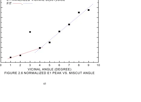
2.6 Normalized E1 peak versus miscut angle for thermally annealed vicinal
(001)Si-SiO2 interfaces……… 45
2.7 Normalized E2 peak versus miscut angle for thermally annealed vicinal
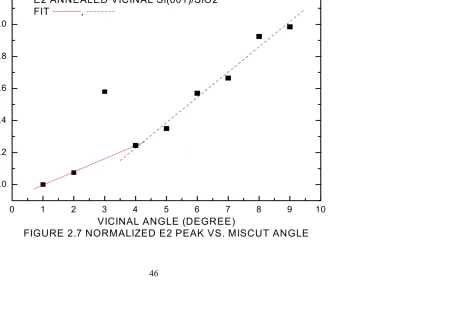
(001)Si-SiO2 interfaces……… 46
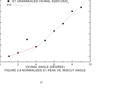
2.8 Normalized E1 peak versus miscut angle for thermally unannealed vicinal
(001)Si-SiO2 interfaces……… 47
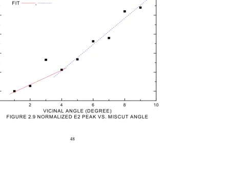
2.9 Normalized E2 peak versus miscut angle for thermally unannealed vicinal
(001)Si-SiO2 interfaces……… 48
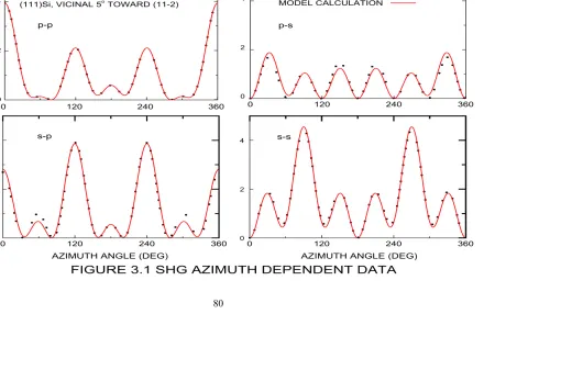
3.1 SHG p-p, p-s, s-p, s-s data versus azimuth angle for vicinal 50 (111)Si
toward (11-2)-SiO2 interfaces……… 80
3.2 SHG p-p, p-s data versus azimuth angle for vicinal 90 (001)Si toward (111)-
SiO2 interfaces………..……….. 81
3.3 Schematic silicon bond picture for Si(111) and Si(001) ……….. 82
……….. 83
3.5 Vicinal 60 Si(001) SHG data-uannealed sample……….. 84
3.6 Vicinal 60 Si(001) SHG data-annealed sample...……….. 85
Appendix A Fig. 1a shows the principle of RDS works………..… 92
Fig. 1b Schematic diagram of a reflectance difference spectrometer………… 93
Fig. 2 Schematic diagram of a polarizer-photoelastic-modulator-analyzer RDS spectrometer……… 94
Fig. 3 a. Pure terrace Si(001) RDS spectrum and b. RDS Spectra of vicinal Si(001) surfaces……… 95
Fig. 4 Step RDS spectra from Fig. 2 and Fig. 3……….. 96
Fig. 5 UHV Si vicinal stepped surface ………. 97
Fig. 6 The first oxide layer at Si-SiO2 interface………... 98
Fig. 7 Neaton’s Si-SiO2 interface model………... 99
Chapter 1. Introduction
1. Overview
The current trend of semiconductor technology demands faster signal
processing speed, less heat dissipation, higher density of devices per chip, lower
defect concentrations for large volume manufacturing, lower leakage currents,
higher time-dependent breakdown voltages, more uniform oxide thicknesses
over larger wafer sizes, more functionality, better performance, and higher
reliability for each device. One simple approach at present is to continue to
reduce the gate dielectric (SiO2) thickness in metal-oxide field-effect transistors.
However, this scheme will no longer work once the gate oxide thickness reaches
the fundamental physical limit of ultralarge-scale-integrated (ULSI) device scaling
of 5 atomic distances by the year 2012.[1-3] At this scale the electrical and
optical properties of the thin oxide become quite different from what one would
expect on the basis of thicker oxides[4], hence a comprehensive understanding
and exact control of the interface become crucial.
Although many scientists and engineers around the world are trying to
circumvent these technological and scientific challenges, investigating for
example the use of high-k dielectrics as a possible replacement for SiO2 or other
types of transistors[4], these approaches have not yet been successful. Also,
although the Si-SiO2 interface has been studied for many decades, many
structure at the interface? Despite many efforts to answer these questions, there
has been no clear resolution of these issues and they are still under debate.
The main goal of the present work is to evaluate various vicinal (001)Si-SiO2
interfaces following various heat treatments by remote, invasive,
non-destructive linear and nonlinear optical techniques and to understand the optical
responses of these interfaces. Our results will help to further characterize these
interfaces by optical means in the future. Specifically, we apply reflectance
difference spectroscopy (RDS) and second harmonic generation (SHG) to study
the optical anisotropy of these interfaces and their interfacial bonding structures,
respectively, and correlate the RD and SHG results. Vicinal Si(001) substrates
introduce local bonding asymmetries at the interface leading to interesting linear
and nonlinear optical responses. From the optical responses arising from these
interfaces we obtain a better understanding of the linear and nonlinear optical
responses of steps, both single and double atomic height. We also obtain a
better understanding of single- and double-domain terraces, which cannot be
distinguished easily using the conventional truncated Fourier series or
complicated tensor-coefficient approaches.
Using the simplified bond hyperpolarizability model (SBHM) of SHG, which
we introduce to describe the anisotropy of SHG intensities, we quantitize and
characterize the interfacial properties in a more precise way and gain further
physical insight about these interfaces. This approach uses four complex
interfacial silicon bonds, to describe the nonlinear polarization of the interfaces
induced by the incoming electromagnetic field to gain physical insight from
azimuth-dependent SHG intensity data and to identify SHG absorption as well as
to obtain information about the origin of SHG. In fact, since some bonds are
equivalent, fewer than four complex hyperpolarizabilities are needed. In contrast,
the conventional phenomenological tensor approach employs a large number of
components to express nonlinear effects, even though symmetry consideration
causes some of the components to vanish. The fact that the tensor approach
also expresses SHG signals as complicated lengthy tensor functions means that
considerable useful information is buried and much of the physical insight that we
can gain from SHG data is lost. As part of the present work we obtain information
about thermal annealing and rapid thermal annealing (RTA) techniques that are
standard industrial methods to reduce defect density, roughness, and strain at
the interfaces. SHG p-p and p-s data indicate interesting changes of complex
hyperpolarizabilities as a result of this processing. The details of these results
will be described in this work and are planned to be published elsewhere.
1.2 Outline of this Dissertation
In Chapter 2 we describe the application of RDS to study the linear optical
anisotropy of vicinal Si(001)-SiO2 interfaces and describe our results. We
compare our results to those obtained by others on clean surfaces in UHV,
cases. From these analogies we are able to take advantage of the
double-domain nature of these interfaces to study SHG at these interfaces using the
SBHM. The results show that a single- to double-height step phase transition
exists at the Si-SiO2 interface as well as on clean surfaces in UHV. We conclude
the chapter with the theory explaining possible step driving mechanisms.
In Chapter 3 we describe our application of SHG to study the chemical
bonding at these interfaces. First we show that the SBHM can describe SHG
anisotropies at the (111)Si as well as the (001)Si cases, and compare the two
cases. The results show that optical responses can also be understood as
classical dipole radiation of induced effective linearly and nonlinearly polarizable
Si bonds. We explain the origin of SHG anisotropy at the interface and the
implications of the unusual one- and three-fold symmetries associated with
atomic steps at the vicinal (001)Si-SiO2 interfaces.
Chapter 4 summarizes our conclusions and lists suggestions for future
1.3 Reference
1. Semiconductor Industry Association: National Roadmap for Semiconductor
71-81 (Sematech, 1997).
2. D. A. Muller, T. Sorsch, S. Moccio, F. H. Baumann, K. Evans-Lutterodt, and
Timp, Nature 399, 758 (1999).
3. M. Schulz, Nature 399, 729 (1999).
Chapter 2. Reflectance Difference Spectroscopy
2.1 Introduction
The Si-SiO2 interface has been intensively studied for many decades, but
fundamental questions remain. These questions gain importance since, from a
technological point of view, the gate oxide thicknesses of transistors are
expected to arrive at the fundamental physical limit of ultralarge scale integration
(ULSI) device scaling of 5 atomic distances by the year 2012. To achieve
expected device performance, functionality, and reliability under such conditions,
exact control of interface properties will become critical, and inevitable.[1-3]
We therefore require a more precise and comprehensive understanding of
the properties of specifically the (001)Si-SiO2 interface at the atomic scale, since
this is the orientation used in technology. In addition to its technological
importance, from a scientific point of view an improvement of our understanding
can lead to further advances in topics such as chemical reactivity, interface
reconstructions, and step phase transitions, as well as providing information
about clean-surface topics such as adatom diffusion, nucleation, film growth, and
heteroepitaxy including the growth of III-V semiconductors on Si for
optoelectronic applications.[4-9]
This work is a comprehensive study of interfaces formed on vicinal (001) Si
simplified bond hyperpolarizability model (SBHM), discussed in detail in Section
3.2, was a direct collaboration involving Powell. However, two distinctions need
to be made. First, (001) Si is the orientation used in technology, and hence is in
principle of considerable more interest to problems currently faced by technology.
Second, (001) is a much more difficult Si orientation to deal with, since in
contrast to the (111) surface, (001) Si exhibits two domains on a macroscopic
scale, and thus the intrinsic terrace contributions are much more difficult to study.
As a result the present investigation deals with the response of vicinal (001)
samples, and is restricted to oxidized interfaces rather than a combination of
oxidized and nitrided interfaces as investigated by Powell.
In this work we are particularly interested in steps, which by entropy occur
on a statistical basis on nominally flat surfaces but can be generated in controlled
densities through the use of vicinal samples, i.e., by deliberately cutting and
polishing surfaces misoriented by various amounts with respect to the (001)
direction. One motivation for studying steps is that they affect electron and hole
channel mobilities in FET structures.[5,6] A second motivation is that, although
step transitions have been studied in great detail on atomically clean surfaces in
ultrahigh vacuum (UHV), essentially no studies have been made concerning
steps at interfaces. These factors prompted us to probe steps and investigate
phase-transition mechanisms, if they exist, at (001)Si-SiO2 interfaces. Optical
techniques in general offer several advantages over conventional surface
investigation mainly by providing a simple, fast, noninvasive way of accessing
steps beneath transparent overlayers. In particular, owing to its sensitivity to
steps, reflectance-difference (-anisotropy) spectroscopy (RDS/RAS) is ideal. We
show here that RDS is not only “step-specific” but also “sub-step-specific”.
Our results are of interest for several reasons. First, our RDS data show
that the oxidized vicinal (001) Si-SiO2 interface exhibits a single-to-double-height
step phase transition near 4° with increasing vicinal angle, which is quite similar
to that observed in ultrahigh vacuum (UHV) and by now well understood
theoretically. However, the UHV transition is driven by localized strain resulting
from Si terrace dimers, which do not exist, or at least do not exist in the same
form, at Si-SiO2 interfaces. We argue that, as in the UHV case, the phase
transition is also due to strain, although details will have to wait until calculations
of the step structure are available. To our knowledge such calculations do not
exist for steps on the Si-SiO2 interface.
Second, we have performed extensive studies of these samples using
second-harmonic generation (SHG), which also reveal the step-phase transition
and in addition are used to provide an additional critical test of the SHBM, which
was previously investigated only for the (111) Si-dielectric interface. Comparing
the results obtained with the two orientations shows distinct differences and also
provides new insight concerning the origin of SHG signals at these interfaces.
angle of incidence and observation of 12°, as opposed to 29° as determined for
(111)Si-dielectric interfaces. This implies that the SHG signal arises at the Si
side of the (001) interface, as opposed to the oxide side for the (111) orientation.
We have also performed spectroscopic ellipsometric (SE) measurements of
these interfaces, but the results are not discussed here since the data were
obtained mainly to verify that the interface widths were small and the sample
properties measured therefore not dominated by interface-roughness effects.
Our results show interesting and unexpected effects that should provide
theorists with an incentive to consider the (001)Si-SiO2 interface in more detail.
This is a goal certainly worth encouraging given the technological importance of
this materials system.
Regarding the rest of Sec. 2.2, Sec. 2.2 describes sample preparation,
experimental apparatus, and methods of analysis, while Sec. 2.3 presents and
discusses the results.
2.2. Optical Anisotropy of Vicinal Si-SiO2 Interfaces: Evidence for Step Phase
Transitions
As discussed in the Introduction, we have investigated the Si-SiO2 interface
by performing a series of linear-optical and SHG measurements on vicinal
(001)Si-SiO2 samples. Specifically, our set consists of (001) samples with offcut
experimental details regarding sample preparation and RD data acquisition, and
how the results are analyzed.
2.2.1 Samples and Sample preparation.
Our experiments were performed on P-doped n-type nominally (001) Si
wafers with resistivities of about 10 Ω-cm and vicinal angles from 1o to 9o
oriented toward the nearest (111) axis. The samples were prepared by a
modified oxide growth technique that is also used to prepare gate
dielectrics.[10,11] The procedures are as follows. First, 100 Å sacrificial oxides
were thermally grown on the Si substrates at a temperature of 900 oC after RCA
chemical cleaning. Next, these oxides were removed immediately after growth in
dilute (1:500) HF. Finally, immediately after stripping 30 Å thermal oxides were
grown at 800 oC. Half of these samples were annealed in N2 at 900 oC for 20
min., and half were saved for control purposes.
Different oxide preparation methods and processing sequences lead to
significantly different degrees of roughness at these interfaces. The variety of
conclusions in the literature are at least partly a consequence of the neglect of
these factors. Accordingly, we paid particular attention to sample preparation.[12]
The micro-roughness of the interface is generally related to the presence of
(SE). The SE-determined interface widths of our samples are about 5Å or less,
indicating that our interfaces are essentially atomically smooth. Hence we rule
out the possibility of artifacts due to rough interfaces.
2.2.2 Experimental Configuration and Principles of RDS
RD data were obtained using a spectrometer with a range of 1.5 to 5.5 eV,
as described elsewhere.[7] Specifically, the configuration consists of a Xe arc
lamp, a focusing mirror, a folding mirror, a quartz Rochon prism, the sample, a
photoelastic modulator operating at 50 kHz, an quartz Rochon analyzer prism, a
condensing mirror, a folding mirror, a 0.1 m focusing-grating monochromator,
and an end-on photomultiplier as shown in appendix A. The output of the
photomultiplier was converted to a voltage, which was used to regulate the
photomultiplier voltage to maintain 10 µm average anode current at the output to
normalize the signals despite a considerable variation in detected intensity over
the 1.5 to 5.5 eV spectral range. The output of the photomultiplier was also
routed to two phase-sensitive detectors operating at 50 and 100 kHz to obtain
the spectral dependences of the relative phase and amplitude, respectively, of
the anisotropy of the near-normal-incidence reflectance of the sample. However,
only the relative amplitudes are used here. At mid-range the configuration can
achieve a signal-to-noise ratio of about 1 part in 105.
incidence with the samples in air. The relative angles of polarizer and modulator
were adjusted to give a zero reading on the 100 kHz phase-sensitive detector
prior to measurement. However, owing to the small signals involved data were
obtained at 4 azimuth angles, nominally 0, 45, 90, and 135°, and subsequently
combined by Fourier analysis first, to ensure that at least one azimuth angle
existed at which a true null could be obtained and second, to eliminate as far as
possible instrument artifacts, since these contribute equally to all spectra
regardless of sample azimuth. The determination of a true null signal at some
azimuth ensures that there exists only one contribution to the optical anisotropy
of the sample, or more accurately no contributions with principal axes at surface
orientations different from that of the main anisotropy arising from the steps.
The optical anisotropy of the samples can be expressed in terms of the
complex normal-incidence reflectance as
∆ ~r / r~ =
+ − R R ~ ~
= ∆ r / r + i ∆θ
R~− = (r~α −~rβ), R~+ =
2 1
) ~ ~ (rα +rβ
where r~α and r~β are the complex reflectances for incident light linearly
polarized along the principal axes α andβ, respectively, of the sample. In our
r
r / ~
~
∆ data, α is defined to be the along the [1 1 0] direction (parallel to the
According to the Fresnel three-phase model, ∆ r~ / r~ can be written in terms of
the interface (or surface) dielectric anisotropy (
ε
α-εβ)d as∆ r~ / r~ = λ πid
4
(
1
− −
s ε
ε εα β
)
where εs is the bulk dielectric function of the substrate and εαd and εβd are the
interface (or surface) dielectric responses along the α and β axes, respectively,
λ is the incident wavelength, and d is the thickness of the interface.[13] Since Si
is cubic, the linear anisotropy arising from the bulk is negligible, and since the
SiO2 overlayer is amorphous, its linear anisotropy is also negligible. Hence the
observed anisotropy originates entirely from the interface, and is expressed as
the effective two-dimensional dielectric response (ε −α εβ)d.
2.2.3 RDS of a Vicinal Surface – General Considerations.
In general, as with clean surfaces the optical anisotropy of the Si-SiO2
interface is expected to arise in principle from a combination of step and terrace
contributions, and thus can be written as
∆r / r = Ft (∆r / r)terrace + Fs (∆r / r)step 2.1
where (∆r / r)terrace and (∆r / r)step are the RD signals from the terraces and steps,
terrace orientations exist, since the Si lattice consists of two chemically identical
interpenetrating fcc lattices rotated with respect to each other by 90°.[see
Appendix A ] If one could create a primitive surface or interface, i.e., one where
all atoms were drawn from only one of the two inequivalent sublattices, the (001)
surface should exhibit twofold rotation symmetry as a consequence of the fact
that the outermost plane of atoms has two bonds upward to the oxide. For
materials such as Si and Ge that crystallize in the diamond structure, the two
sublattices are chemically identical, so it is impossible to chemically distinguish
them and prepare a singular surface through the use of chemistry as is the case
of III-V compound semiconductors. Thus for (001)Si-SiO2 interfaces that are not
deliberately miscut by a sufficiently large angle any macroscopic surface area,
such as that covered by an incident optical beam, must consist of statistically
equal areas of interface atoms drawn from each of the two different sublattices,
although the individual domains themselves will exhibit twofold rotational
symmetry. Thus a macroscopic region of the (001)Si-SiO2 interface will exhibit
overall fourfold rotation symmetry, which will not be detected by linear-optical
probes since the linear-optical response is described by a second-rank tensor.
For clean, on-axis surfaces in UHV this double-domain behavior leads to
combined symmetries of type (2×1) or (1×2) as observed by reflection
high-energy electron diffraction (RHEED). These symmetries result from the
directions. While the exact microscopic nature of (001)Si-SiO2 interfaces is
clearly more complicated than that of the clean surface and is still under debate
(see below), a given single domain should still be optically anisotropic. Thus a
primitive interface should yield an anisotropy contribution for all miscut angles
down to and including zero. However, given the strength of the Si-O bond and
therefore the energy difference between bonding and antibonding orbitals, it is
not clear that any terrace optical anisotropy will be particularly strong in our
accessible spectral range of 1.5 to 5.5 eV. The early reflectance measurements
of Chiarotti et al. certainly suggest that any such anisotropy will be relatively
featureless in this spectral range at best.
Step contributions may be different, but are complicated by the fact that at
least four types of step reconstructions, two single-height and two double-height,
can occur. Each of these can run in orthogonal directions across the surface.
Even though no models so far have been proposed to describe the detailed
atomic structure of steps at Si-SiO2 interfaces, given the strong binding energy of
the Si-O bond it is clear that the bonding configurations will be entirely different
from those on clean surfaces. The driving force here should be to maximize the
number of nominally “dangling” bonds-oxygen deficient bonds- (those that at the
interface involve oxygen atoms) rather than minimizing them, and also to satisfy
interface energy minimization.[32] As a result it is not clear that an interface
anisotropy analogous to the surface-state anisotropy observed on clean surfaces
above. Nevertheless, by geometric arguments any step contribution should be
optically anisotropic, although if this arises from strain or lifetime effects it may
not be possible to distinguish one type of step from another in the spectral data.
Since the different step configurations are expected to have different
formation energies, for sufficiently large vicinal angles we would expect one type
of step to be preferred, with its enthalpy overcoming the entropy-driven
production of single-height steps that is expected to occur for small vicinal
angles. This is well known in the case of clean surfaces in UHV, where the
step-phase transition occurs at miscut angles of about 3 to 4° and is driven by the
lower energy of a particular double-height step. The response of the oxidized
interface with increasing vicinal angle should therefore be qualitatively similar to
that of the clean surface: a small, possibly vanishing anisotropic response for
small vicinal angles and a more rapidly increasing one at larger angles. Thus the
general behavior expressed by Eq. (2.1), which has been shown to be valid for
the UHV case, is expected to apply here as well.[12]
2.3 Experimental Results and Discussion.
To determine the optical anisotropy of vicinal silicon interfaces, we obtained
RD spectra of oxidized vicinal interfaces prepared and measured as described
above. A representative set of data is plotted in Figs. 2.1 and 2.2 for the
spectra are calculated as a Fourier transform of four spectra each taken at
azimuth angles separated by 45° and with an averaging time of 2 s per data
point. The inversion angle of the Fourier analysis was first chosen to obtain a
null spectrum if possible (not shown), and a spectrum corresponding to the
maximum signal. The purpose of this approach was to ensure that null spectra
could be realized, i.e., that only one type of optical anisotropy was effectively
present. This was observed to be the case for all data except those taken on
unannealed 3 and 7° samples, which showed small residual structures at the
(E0’, E1) and E2 spectral features near 3.4 and 4.2 eV, respectively, for reasons
that are not clear.
The spectra are shown for increasing vicinal angle and are offset for clarity.
These spectra show two general features, one related to the (E0’, E1) complex
and the other to the E2 transitions. It is clear from these data that to within our
signal-to-noise capability these lineshapes remain essentially constant and
simply increase in magnitude with increasing miscut angle as shown in Figs
2.6-2.9 . This is consistent with our strain argument given above. Thus unless all
possible contributing processes have exactly the same lineshape to within our
ability to determine it, not a likely occurrence, these data indicate that only one
mechanism is responsible for the observed anisotropy of these interfaces from 1°
To begin, analysis can therefore be reduced to examining the behavior of
these amplitudes with miscut angle. We first assume that all lineshapes are
equivalent to that shown for the annealed 9° sample in Fig. 2.2 with the possible
exception of baseline offsets, then use a least-squares fitting procedure to
determine the magnitude of the 9° component in each of the other spectra.
Since baselines vary somewhat from spectrum to spectrum, the baseline
(assumed to be a constant) and the scaling amplitude were both treated as
adjustable parameters in this analysis. The amplitudes so determined are shown
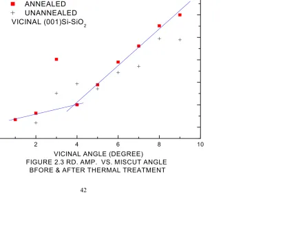
in Fig. 2.3. The uncertainty of these magnitudes, as determined by repeating the
measurements on different areas of the wafers, is about 3% of the full-scale
value. While the amplitudes of the oxidized samples show a relatively smooth
linear increase, those of the annealed samples shows a distinct break at 4°. The
datum for the 3° sample is clearly anomalous. However, this is a real effect as
the unusual RD response was observed for several runs. A recheck of the
orientation of this sample showed that it was indeed 3°, and not 6° as might be
inferred from its value. We note that a similar anomaly at a miscut angle of 3°
was also seen in XPS measurements[23], suggesting the existence of coherence
effects in terrace widths and /or step configurations at “special” angles even in
interfaces, as previously noted in several similar investigations of clean surfaces
in ultrahigh vacuum (Ref Whitman, possibly Hoppe and Wijers). This
was interpreted as facet formation at the interface. [23] The mechanism is still not
clear and requires futher investigation.[23]
Figure 2.3 also shows that the interfaces are rough compared with the ones
after treatment and less ordered as indicated by data randomness before thermal
annealing treatment. It turns out that the trends do follow a straight line but with a
large fluctuation before thermal annealing. However, upon thermal annealing the
optical anisotropy becomes “linearly” proportional to the vicinal crystal miscut
angle as shown in Fig. 2.3. In particular, the RD trend before the annealing
treatment also implies that the interfaces are in the mixed stepped phase, which
will be explained by the theory in the following.
We now consider the implications of these results. Our analysis will follow
in part that of Jaloviar et al.[14] since RD data for clean vicinal (001)Si surfaces
in UHV show similar trends, and a comparison of the UHV and oxidized cases
will aid the understanding of both sets of data. The UHV data show a similar
lineshape invariance with respect to miscut angle, although the lineshape itself
exhibits some differences with respect to that obtained for the Si-SiO2 interface.
One major discrepancy is the appearance of significant anisotropy below 3.4 eV
in the UHV case, which implies substantial surface absorption since Si is
essentially transparent in this spectral region. This low-energy absorption is due
to states that exist on the clean surface but are not expected to be present (and
higher-lying structures are similar in both clean-surface and oxidized-interface cases
and are expected to originate for similar reasons. Since all features increase
monotonically with increasing vicinal angle, we can consider these features to be
connected in some way to steps. This includes those features that are clearly
due to surface states. In principle this also includes terrace contributions, since
steps can cause one terrace orientation to be favored over another or vice versa.
Since the UHV lineshapes are also invariant, we plot without regard to the
actual mechanism giving rise to the anisotropy at a given energy, and therefore
without loss of generality, the amplitude of |∆r /r|uhv at 3 eV in Fig. 2.4. The
trend is the same, general increases exhibiting a break in the slope with only the
lower-miscut line intersecting zero. Whether the 3° anomaly seen in Figs. 2.1
and 2.2 exists for clean surfaces in UHV is not established since Jaloviar et al.
did not report data on a sample miscut by 3°. Since in UHV the single- to
double-height phase transition occurs at a vicinal angle of about 4°, the implication is
that the contribution for the oxidized interfaces are also coming from steps.
As a result of STM measurements [20] considerable information is available
about the nature of clean vicinal surfaces in UHV. Below about 3o the surface is
essentially double-domain, terminated by a combination of (2x1) and (1x2)
surface becomes single-domain with the terraces separated by
double-atomic-height DB steps in the notation of Chadi [21]. At 3° the surface consists of a
coexistence of about 40% DB steps and 60% SB steps, leading to a gradual
structural phase transition regarding SB and DB steps. As known from the
previous studies[14], both SB and DB steps contribute significantly to RD signals.
In particular, the rebonding necessary to create a SA step does not perturb the
nearby terrace atoms, and therefore one would expect SA steps to have
negligible RD contribution. Rebonding effects on RD spectra have been
discussed in great detail in Ref. 14, and are supported by the first-principles
calculations of Schmidt et al.[18,19] In addition, the intersection point in Fig. 2.4
implies that DB and SB steps are coexistent and optically indistinguishable on the
samples miscut at 3o angle, which is in excellent agreement with the STM
results.[20]
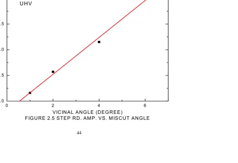
A further close examination of RD step spectra reveal a straight line. These
are shown in Fig. 2.5, and clearly imply that there exist two “almost identical”
types of steps associated with optical anisotropies, and that the optical
anisotropy is “linearly” proportional to the crystal vicinality, in other words, step
density. If the straight line are extrapolated, it intercept the y-axis at a negative
value as the vicinal angle approaches zero. The negative value suggests that the
terrace effect was somewhat over-compensated in Ref. 14 as a result of the RD
spectrum. Besides, the higher intercept at lower vicinality is more evidence of
double-domain behavior. For clean surfaces in UHV, these two types of steps
( rebonded SB and DB ) [21] are almost identical except that the step height as
well as the nearest dimers on the terraces above and below the steps are
different. It is plausible that the intercept in Fig. 2.5 can be attributed to the
residual terrace contribution. The rebonded SB and DB steps to which we refer
were thoroughly illustrated and theoretically studied by D. J. Chadi.[21].
Nevertheless, it is quite legitimate to apply the same interpretation to the RD
trend in Fig. 2.3 as in Fig. 2.4. With this interpretation, double-domain
single-atomic height steps dominate at oxidized interfaces with miscut angle less than
4o while single-domain double-atomic height steps prevail at interfaces with
miscut angle greater than 4o. The agreement between the two sets of data shows
that optical anisotropies of both clean and oxidized surfaces are in part induced
by similar effects, although the atomic structures of steps, dimers, and terraces at
oxidized silicon surfaces are different from those at clean ones. Hence, we term
these structures as being due to quasi-steps, quasi-dimers, and quasi-terraces.
These structures can be approximately visualized by assuming that oxygen
atoms incorporate at bridge sites [24] that would correspond to dimers on the
clean surfaces (one oxygen atom incorporated between every two silicon atoms
in silicon tetrahedral structure unit).
structural model. However, despite enormous efforts to establish an accurate
model, the conclusions from various studies of many experimental techniques
are elusive. Nevertheless, most of these studies agree that there exist two
distinct interface regions. One is about 1 to 2 monolayers thick with Si atoms in
intermediate oxidation states, i.e, Si+1(Si2O), Si+2(SiO), and Si+3(Si2O3). The
other is a compressed region extending about 20 Å into the bulk amorphous α
-SiO2 layer. It is well established that core-level photoelectron spectroscopy (PES)
enables us to obtain the information about the density and distribution of these
intermediate oxidation states (suboxides) but no corresponding spatial
information of the suboxides.[12] On the other hand, reflection high energy
electron diffraction (RHEED), x-ray diffraction (XRD), grazing incident x-ray
scattering (GIXS), and transmission electron microscopy (TEM) can only give us
precise spatial information about the first layered suboxides, because the
amorphous nature of the nearby bulk SiO2 material limits the resolution that we
can obtain.
In order to construct a model, several criteria must be met. First, the
interface should exhibit minimum strain and be about 5 Å wide (the strain results
from the volume mismatch between Si and SiO2).[24] Second, the near-interface
structure should be aβ-tridymite-like interfacial crystalline phase, as shown by
GIXS,[24] XRD,[26] and TEM.[27,28] Third, nearest neighbors should exhibit
chemical shifts due to intermediate oxidation states, as observed by PES.[24]
interface (1 per 104 interface atoms) as shown by electrical measurements, such
as capacitance-voltage measurements.[29] Finally, the density and distribution
of the intermediate oxidation states should be that shown by PES[24]
Pasquarello, Hybertsen, and Car [24] proposed models that meet all these
criteria. However, it is not possible to choose uniquely among their models since
spatial information about the suboxides is not available. From an atomic orbital
bonding point of view, the silicon (oxygen) atomic bonding orbital is structurally
4-fold-symmetric (2-4-fold-symmetric). Several of their models meet the above
requirements.
This situation changed recently with advances in electron energy loss
spectroscopy (EELS), since this has now made it possible to obtain localized
spatial information regarding suboxides and their electronic properties. Based on
the previous criteria and the new EELS spectra,[2,30] a new model was
proposed by Neaton, Muller, and Aschcroft. This is a hybrid of the models of
Pasquarello et al.[24] The Neaton et al. model in Appendix A predicts the same
theoretical unoccupied projected density of states of the oxygen atoms (O
p-UDOS) that is observed for the intensity profiles of the O Kedges measured by
EELS.[30]
In addition, Buczko et al. [31] and Tu et al. [32] applied first-principles ab
initio calculationsand quantum Monte Carolo simulations, respectively, to explore
fact, a 2x1 stripe phase terrace (row pattern of O bridges) as shown in Appendix
A.[31,32] This is consistent with X-ray diffraction[25] and RHEED data.[33] The
Neaton et al. model not only encompasses this aspect but also predicts many
interface properties that agree quite well with the previous experiments. These
studies indeed put a firm footing on the Neaton et al. model and the conclusions
about the structure of the first oxide layer.
Moreover, Ourmazd et al. [27,28] used TEM to demonstrate the presence of
a c-SiO2-like layer at the interface and a 90o (0o) rotation of the c-SiO2 layer
across a single (double) step on nominal Si-SiO2 samples. This suggests similar
atomic bonding structures exist at both clean and oxidized surfaces.
Furthermore, Rochet [34] et al. showed that double steps exist at the oxidized
surface with a 5o miscut angle even though their sample preparation was not
standard. Wantanbe et al. [29] and Cai et al. [30] used scanning tunneling
microscopy (STM) to investigate the local leakage current through ultrathin SiO2
layers. Their STM images imply that B-type steps still exist even under thin oxide
films. All these evidences about steps and terraces underlie our interpretation of
the RD spectra of oxidized interfaces.
Since thermal oxidization transforms -Si-Si- bonds into -Si-O-Si- bonds, the
angle of the -Si-O-Si- bonds often varies slightly from one site to another.[24,31]
As a result the contributions from quasi-terraces are small compared with those
from quasi-steps because of the cancellation due to both double-domain and
Fig. 2.1 receives most of its contribution from steps rather than
quasi-terraces, especially at low crystal vicinality. On the other hand, the spectrum in
Fig. 2.5 is a pure step anisotropy calculated by removing the terrace contribution
from the RD spectra. The different slope constant ratios in Figs. 2.3 and 2.4
result from the fact that the electronegativity of oxygen upon incorporation leads
to similar but different polarizabilities that are responsible for most of the
anisotropies observed for both oxidized and clean silicon surfaces. It is very
likely that these RD signals arise from the region near the first oxide layer, since
this region still preserves Si crystalline order. Long-range order is lost only above
the first layer.
It should be noted that the step-driving mechanisms in both cases are
almost the same, since the common intersection point indicates the coexistence
of SB and DB steps that depend strongly on the atomic bonding structures in a
topological rather than a chemical manner. Rossow et al. [37,38] performed a
RDS study on RCA-cleaned vicinal Si(001) surfaces (H terminated) and found a
surprising similarity between H-terminated and our O-terminated lineshapes.
This implies that the observed optical anisotropy is more atomic-bonding
structure-specific than chemical-termination-specific.
To put it more directly in terms of the driving mechanism, one can apply a
thermodynamic formalism to describe surface morphology and the associated
thermody-showed that the thermodynamic states that dictate Si(001) surface morphology
can be described by the Hamiltonian.
H H SB E
( )
Sl E( )
Sl strainstep +
+
= ( ) or
H =H(DB)+Estep
( )
DB +Estrain( )
DB 2.2(
)
[
]
∑
− + − + − −= ⊥ −
i i i i c hihi
l h h
h SB
H( ) λ 1 κ 2 2ε 1 δ , 1 2.3
(
) (
)
[
]
∑
− + − − + − −= ⊥ −
i i i c hihi hi l
h h DB
H( ) λ 1 2ε 1 δ , 1 λ|| 1 δ 1,2 2.4
( )
Sl =Estrain(1)
(
2 2) (
2 2) (
ln[
) (
(
cos 2)
)
]
0 l λ l l πa πp
λ − σ 2.5
( )
Sl =Estrain(2)
(
2l)(
a 2l)
2[
(
3 l)
(
a 2l) (
(
tan p 2)
)
]
d
d λ λ π
λ − σ 2.6
( )( )
( )
|| . (Sl) 1 2 εp σEexstrain = , Eex.strain(DB)=εσ⊥, β =
( ) (
1 KbT)
( )
Sl =Estep
(
λSA+λSB)
2l,Estep( )
DB =( )
λDB 2l 2.7( )
( ) (
2)
ln(
(
)
)
(1)( )
(2)( )
. ( )max H E Sl E Sl E Sl
l T K Sl E Sl
F = step − b λ SB + strain + strain + exstrain
2.8
( )
DB E( ) (
DB K T 2l)
ln(
max(
H)
)
E . (DB)F = step − b λ DB + exstrain 2.9
The step phase boundary is given by F
( )
Sl −F( )
DB =0 2.10where F is Helmhotz free energy per unit area and λmaxis the maximum
calculated using the transfer-matrix method, [40-42]
where for ZH( )SB
h
(
(
) (
[
)
]
)
(
[
]
)
(
[
(
, ')
]
)
' 2 1 2 exp exp 2
exp− β κ h−l −β λ⊥ h−h −β εc −δhh
(
)
[
(
)
]
(
' 2)
2
exp− β κ h −l h'
where for ZH( )DB
h
(
exp−(
β 2)
[
λ||(
1−δh,2l)
]
)
(
exp−β[
λ⊥h−h']
)
(
exp−β[
2εc(
1−δh,h')
]
)
(
)
[
(
)
]
(
exp− β 2 λ||1−δh',2l)
'h
Here, H is the transfer-matrix element associated with H(SB) and H(DB)
respectively, hi represents the fluctuation of the ith segment of the ledge front at
a temperature T, λ⊥ is the energy cost per unit length of a ledge created in the
perpendicular direction, λ|| is the energy of breaking the DB step into a pair of SA
and SB steps, εc is the creation energy of a corner in a jagged ledge, and
β=
( ) (
1 KBT)
. The quadratic term in H(SB) originates from the second term ofthe strain relaxation energy Estrain(1)
( )
Sl as well as E( )
Slstrain
) 2
( . It only applies to single
(Sl) steps in that Estrain =0 for the double (Dl) stepped surface. Estrain
( )
Slreaches its minimum for a surface with steps equally spaced.
harmonic approximation [41] of Estrain
( )
Sl ,[
( )
2]
[
( )
4]
16 3
8l a λd l a
λ
κ = σ + where
( )
SlEstrain(1) (E
( )
Slstrain
) 2
( ) is the first-order (second-order) strain relaxation energy. 0
λ
is the creation energy per unit length of a domain wall due to dangling bonds,
local deformation, and other such factors, λσ is the coefficient of long-range
force-monopole interaction, which depends on the particular pattern of the stress
domain, the magnitude of anisotropy in σij stress tensor, and the specific bulk
elastic constant. λd is the coefficient of the short-range force-dipole interaction,
which is significant for SA and SB steps.
The first term inEstrain(2)
( )
Sl is the force-dipole interaction term and the secondthe second-order strain energy associated with the stress-domain
interaction.Eex.strain is the external applied strain energy,ε = the external applied
strain, σ|| (σ⊥) is the stress tensor along (perpendicular to) the surface dimer
bond direction, λSA, λSB, and λDB are the step formation energies per unit length
for the SA, SB, and DB steps, and a is a microscopic cutoff length of a Lorentian
broadening of the force density fj
( )
ρ :[39]( )
(
)
(
)
+ − − ± = ia x x x x Ffj o
0 0 1 Im δ ρ
Equation (9)* is a function of
(
T,P,l)
or(
T,P,θ)
can be used to describe the UHVstep transition, which is only valid for the temperature range 3000-5000C.[42] The
external strain ε is applied to the surface, then the widths of alternating 2x1 (or
1x2) domains will become
(
1+P)
land(
1−P)
l respectively. When thetempera-ture is low or at absolute zero, the step thermal fluctuation energy in (2.9) is
negligible and free energy is dictated by the strain-domain relaxation,
force-mutipole interactions, and step formation energies. As a result, DBstepped
surfaces have a lower free energy than Sl stepped surfaces for l<lc1(or θ >θc1).
On the contrary, DB stepped surfaces have higher free energy than Sl stepped
surfaces for l >lc2 (orθ <θc2). For lc1 <l <lc2( or 0 1 0
2 =2.5 < < c =3
c θ θ
θ ) mixed
stepped surfaces having lower free energy than either of them are favorable.[41]
As the temperature rises, the step thermal fluctuation energy is no longer
negligible, the range of critical vicinal miscut angle (θc2,θc1) becomes bigger, and
thus there occurs no distinct step phase transition above a certain temperature.
In other words, the step phase transition is gradual.[41] Although the theoretical
calculation of (θc2,θc1)[41] and the step formation energies are still not accurately
known, this model can account for most experimental results.It not only can be
applied to the UHV case but also to the “oxidized” one, except that all the
parameter values are different and λ0 is the creation energy per unit length of a
domain wall due to oxygen-deficient bonds, local deformation, and other such
factors. Therefore the step driving mechanism for both cases are almost the
instance, there exists a localized strain[42] near the Si-SiO2 interface because
of lattice mismatch before thermal annealing treatment. The localized strain is
equivalent to the external applied strain at the interface, as a consequence,
leading to a larger (θc2,θc1) range. Therefore, the RD signals in Fig. 2.3 indicate
the presence of mixed stepped interfaces before the annealing treatment.
However, after the annealing treatment the localized strain is reduced[42] and
the (θc2,θc1) range becomes smaller, resulting in the distinct step phase
transition shown in Fig. 2.3.
At present, experimental techniques are still unable to provide us with better
step-image resolution, which hinders current progress in theoretical
first-principles calculations of step properties at buried interfaces. Nevertheless, the
atomic bonding topology plays a pivotal role in interface thermodynamics.
Consequently, we hope that the understanding obtained from RDS and other
techniques will further stimulate experimental and theoretical studies in a more
systematic way in the future although the structures and energies of oxidized
steps are presently unknown.
We conclude this section by noting that several of our interpretations are not
only consistent with various recent experiments but also with theories available in
the literature. Renaud et al.[25]and Tsu et al.[33] employed grazing incident x
ray scattering and RHEED techniques, respectively, to demonstrate that there
Tu and Tersoff applied a Monte Carolo simulation to determine Si-SiO2 interface
structures by minimizing interface energy. The optimal interface structure they
found consists of an ordered array of (2x1) -Si-O-Si- bridges with low strain
energy.[32] In summary, using RDS techniques, we are able to identify the
existence of the steps at the Si-SiO2 interfaces optically. Steps, in fact, consist of
domain single-atomic height steps as well as single-domain
double-atomic height steps, of which the density varies linearly with respect to the
vicinality of the silicon substrate. A “gradual” step phase transition was also
observed, which is in good agreement with recent experiments by other
techniques and theoretical predictions. [20,42]
In general the optical anisotropy of cubic semiconductors originates from
the local field effect, which is caused by the broken symmetry (or reduced
symmetry) of the interface and specifically of the difference in screening across
the interface. These effects are aided by bonding charge transfer near the
interface, which tends to minimize the interface energy thermodynamically, and
interface chemical termination as well as strain, which affects the electronic
polarizability of near-interface atomic bonding structures.[18,19,43,44] Although
the conclusions drawn here agree well with the studies reported in the literature,
a systematic theoretical investigation of optical anisotropy of the oxidized vicinal
silicon surfaces is still not available. In principle, interface (or surface) induced
and unambiguous interpretation of RDS lineshapes still relies entirely on the
systematic theoretical study based on first-principles calculations. The present
work is intended to pave the way for further progress in this direction.
The present study of steps at the interface should also shed light on
heteroepitaxy on silicon, which has been explored extensively since the 1980s.
The double steps at the interface can be used to avoid antiphase domains that
occur in heteroepitaxy.[48] Hence the better understanding of the atomic steps
will be of crucial importance in this application as well.
2.4. ACKNOWLEDGMENTS
It is a pleasure to acknowledge support of this work by the Office of Naval
Research under Contract No. 00014-93-1-0255 and by the Army Research Office
under Contract No. TCN 97-184, J. -F. T. Wang would like to thank Joan N.
O’Sullivan at the Microelectronics Laboratory of N. C. State University for her
assistance in sample preparation and also would like to thank committee
members Professor Gerald Lucovsky and Professor Carton M. Osburn for their
2.4 References
1. Semiconductor Industry Association: National Roadmap for Semiconductor
71-81 (Sematech, 1997).
2. D. A. Muller, T. Sorsch, S. Moccio, F. H. Baumann, K. Evans-Lutterodt, and
Timp, Nature 399, 758 (1999).
3. M. Schulz, Nature 399, 729 (1999).
4. G. D. Wilk, R. M. Wallace, J. M. Anthony, J. Appl. Phys. 89, 5243 (2001).
5. T. J. Thorton, J. M. Fernandez, S. Kaya, P. W. Green, K. Fobelets, Appl.
Phys. Lett. 70, 1278 (1997).
6. S. M. Goodnick,D. K. Ferry, and C. W. Wilmsen, Z Lilintal, D. Fathy, and
O. L. Krivanek, Phys. Rev. B 32, 8171 (1985); A. Pirovano, A. L. Lacaita,
G. Zandler and R. Oberhuber, IEEE Trans. Electron Devices 47, 718
(2000).
7. D. E. Aspnes, J. P. Harbison, A. A. Studna, and L. T. Florez, J. Vac. Sci.
Technol. A 6, 1327 (1988).
8. D. E. Aspnes, J. P. Harbison, A. A. Studna, and L. T. Florez, Appl. Phys.
Lett. 52, 957 (1988).
9. I. Kamiya, D. E. Aspnes, H. Tanaka, L. T. Florez, J. P. Harbison, and R.
10. A. H. Carim, A. Bhattacharyya, Appl. Phys. Lett. 46, 872 (1985).
11. H. Niimi, G. Lucovsky, J. Vac. Sci. Technol. B 17, 2610 (1999).
12. F. J. Himpsel, D. A. Lapiano-Smith, and J. F. Morar, J. Bevk, in The
Physics and Chemistry of SiO2 and the Si-SiO2 interface 2, edited by C.
R. Helms and B. E. Deal (Plenum Press, New York, 1993), p. 237
13. J. D. E. Mcintyre and D. E. Aspnes, Surf. Sci. 24, 417 (1971).
14. S. G. Jaloviar, Jia-Ling Lin, V. Zielasek, L. McCaughan, and M. G.
Lagally, Phys. Rev. Lett. 82, 791 (1999).
15. L. S. O. Johansson, R. I. G. Uhrberg, P. Martensson, and G. V.
Hansson, Phys. Rev. B 42, 1305 (1990).
16. R. I. G. Uhrberg, G. V. Hansson, J. M. Nicholls, and S. A. Flodström,
Phys. Rev. B 24, 4684 (1981).
17. S. G. Davison and M. Stęślicka, Basic Theory of Surface States, ( Oxford
University Press, London, 1996).
18. W.G. Schmidt and F. Bechstedt, Phys. Rev. B 63, 0453221 (2001).
19. W.G. Schmidt, N. Esser, A. M. Frisch, P. Vogt, J. Bernholc, F. Bechstedt,
M. Zorn, Th. Hannapel, S. Visbeck, F. Willing, W. Richter, Phys. Rev. B
20. B. S. Swartzentruber, N. Kitamura, M. G. Lagally, and M. B. Webb,
Phys. Rev. B 47, 13439 (1993).
21. D. J. Chadi, Phys. Rev. Lett. 59, 1691 (1987).
22. X. Chen and J. M. Gibson, Appl. Phys. Lett. 70, 1462 (1997)
23. M. Niwano,H. Katakura,Y. Takeda,Y. Takakuwa, N. Miyamoto, M. Maki,
J. Vac. Sci. Technol. B 10, 339 (1992)
24. A. Pasquarello, M. S. Hybertsen, R. Car, Nature 396, 58 (1998);
Pasquarello ibid, Appl. Phys. Lett. 68, 625 (1996); A. Pasquarello, M. S.
Hybertsen, R. Car, Phys. Rev. Lett. 74, 1024 (1995).
25. G. Renaud, P. H. Fuoss, A. Ourmazd, J. Bevk, B. S. Freer, P. O. Hahn,
Appl. Phys. Lett. 58, 1044 (1991).
26. L. K. Robinson, W. K. Waskiewicz, R. T. Tung, and J. Bohr, Phys. Rev. Lett.
57, 2714 (1986).
27. A. Ourmazd, D. W. Taylor, J. A. Rentschler, and J. Bevk, Phys. Rev. Lett.
59, 213 (1987).
28. A. Ourmazd, J. A. Rentschler, and J. Bevk, Appl. Phys. Lett. 53, 743 (1988).
29. S. C. Witczak, J. S. Suehle, and M. Gaitan, Solid State Electron. 35, 245
(2000)
31. R. Buczko, S. J. Pennycook, and S. T. Pantelides, Phys. Rev. Lett. 84,
943 (2000).
32. Y. Tu and J. Tersoff, Phys. Rev. Lett. 84, 4393 (2000).
33. R. Tsu, A. Filios, C. Lofgren, K. Dovidenko, C. G. Wang, Electrochem. And
Solid State Lett. 1, 80 (1998).
34. F. Rochet, M. Froment, C. D’anterroches, H. Roulet, and G. Dufour, Pil.
Mag. B, 59, 339 (1989)
35. H. Watanable, K. Fujita, and M. Ichikawa, Appl. Phys. Lett. 72, 1987
(1998).
36. Q. Cai, Y. F. Hu, S. T. Hu, and X. Wang, J. Vac. Sci. Technol. B 18, 2384
(2000).
37. U. Rossow, L. Mantese, and D. E. Aspnes, J. Vac. Sci. Technol. B 14, 3070
(1996).
38. L. Mantese, U. Rossow, D. E. Aspnes, Appl. Surf. Sci. 107, 35 (1996).
39. O. L. Alerhand, David Vanderbilt, R. D. Meade, and J. D. Joannopoulos,
Phys. Rev. Lett. 61, 1973 (1988).
40. O. L. Alerhand, A. Nihat Berker, J. D. Joannpoulos, David Vanderbilt, R. J.
41. T. W. Poon, S. Yip, P. S. Ho, and F. F. Abraham, Phys. Rev. Lett. 65,
2161 (1990).
42. E. Pehlke, J. Tersoff, Phys. Rev. Lett. 67, 465 (1991). E. Pehlke, J. Tersoff,
Ibid 67, 1290 (1991)
43. J. T. Fitch, C. H. Bjorkman, G. Lucovsky, F. H. Pollak, and X. Yin, J.
Vac. Sci. Technol. B 7, 775 (1989)
44. D. E. Aspnes and A. A. Studna, Phys. Rev. Lett. 54, 1956 (1985)
45. W. L. Mochán and R. G. Barrera, Phys. Rev. Lett. 55, 1192 (1985)
46. A. I. Shkrebtii and R. Del Sole, Phys. Rev. Lett. 70, 2645 (1993).
47. T. Yasuda, D. E. Aspnes, D. R. Lee, C.H. Bjorkman, and G. Lucovsky,
J. Vac. Sci. A 12, 1152 (1994).
48. H. Kroemer, Heteroepitaxy on Silicon, edited by J. C. C. Fan and J. M.
Poate, Mat. Res. Symp. Proc. Vol. 67, 3 (1986).
49. The Physics of SiO2 and its Interfaces, edited by S. Pantelides
(Pergamon Press New York, 1978).
50. The Physics and Chemistry of SiO2 and the Si -SiO2 Interface, edited by C.
R. Helms and B. E. Deal (Plenum Press, New York, 1988).
Vac. Sci. Technolol B19, 589-592 (2001).
52. K. Hirose, H. Nohira, K. Sakano, T. Hattori, Appl. Surf. Sci. 166, 455-459
2 3 4 5 0.0
0.5 1.0 1.5
3O
1O 9O
VICINAL (001)Si-SiO2 UNANNEALED
10
3 (
∆
R / R)
ENERGY (eV)
2 3 4 5 0.0
0.5 1.0 1.5
VIC IN AL (001)Si-SiO2 AN N EALED
1o 9o
10
3 (
∆
R / R)
EN ER G Y (eV)
0 2 4 6 8 10 0.0
0.2 0.4 0.6 0.8 1.0 1.2
ANNEALED
UNANNEALED
VICINAL (001)Si-SiO
2LIN
ESH
APE NORMAL
IZED FRACTION
VICINAL ANGLE (DEGREE)