PD Analysis in Cylindrical Void With Respect To
Geometry of the Void
C Sunil Kumar1, Dr. B. Ramachandra2, Manohara H C3
Assistant Professor, Department of E&E, PESCE, Mandya, Karnataka, India 1 Professor & HOD, Department of E&E, PESCE, Mandya, Karnataka, India 2 Assistant Professor, Department of E&E, PESCE, Mandya, Karnataka, India 3
ABSTRACT: Partial discharge is an important phenomenon to be considered while studying insulation failure. Analysing
PD characteristics and the detection of PD activity will help in improving the performance of insulator. In high voltage power system it is necessary to monitor the PD activity inside an insulator continuously. As the applied voltage increases the PD activity increases as theelectric stress across the void becomes more than the electric stress across an equivalent distance of dielectric [1]. The deterioration depends on the applied voltage and the number of discharge [2]. In this work an electric circuit model of an epoxy resin with void of cylindrical shape is considered for realization of partial discharge activity inside the insulator with the application of high voltage using MATLAB Simulink environment. The results obtained with variation in the parameters of the void such as radius, height and volume of the cylindrical void as an impurity is analysed.
KEYWORDS: Partial discharge (PD), void, High voltage (HV), Ca, Cb, Cc, r-radius and h-height.
I.INTRODUCTION
Solid dielectrics or insulation get damaged when breakdown occurs. There are various mechanisms in which breakdown occurs. In case of partial discharge, the continuous discharge causes progressive deterioration and ultimate failure [3]. The deterioration depends upon the applied voltage and number of discharge [2]. According to IEC (International Electro technical Commission) Standard 60270, Partial discharge is a localized electrical discharge that only partially bridges
the insulation between conductors and which may or may not occur adjacent to a conductor [1]. PD activity affects the performance of the insulator used. Therefore, it is very important to analyze the various failure mechanisms in case of solid dielectric through non-destructive testing mechanism. Detection of discharges can be made through various methods. The geometry of void present inside the insulation affects the PD activity by creating a weak zone [5]. In this work, an electrical circuit model of an epoxy resin as an insulator with avoid of cylindrical shape is considered for the analysis of PD activity inside the insulator with the application of high voltage using MATLAB Simulink software, as shown in figure 2. In this study, apparent charge transfer with respect to variation in the dimensions of the void (r, hand volume), PD amplitude with variation in the dimensions of the void for both positive and negative half cycle of the applied voltage is studied. Also the rise and fall time of the PD pulse are calculated and frequency content of the observed PD pulse is studied.The results obtained with cylindrical void as an impurity is analysed so as to determine the effect of geometry of cavity or void on PD activity.
II. RELATED WORK
1. Continuous monitoring of PD activity is essential to ensure the effective performance of the insulator. From [5], the variation of apparent charge transfer with variation in the dimensions (ℓ, b, t and volume) of the void, PD amplitude
2. Detection and measurement of partial discharge is necessary to ensure reliable operation of equipment. From [7], the maximum amplitude of PD, PD pulses at different applied voltages, number of PD's with respect to phase angle, apparent charge transfer for different applied voltages and frequency content of the observed PD pulse is studied. The results obtained with cylindrical and cubical void as an impurity is compared and analysed. It is observed that the amplitude of PD is maximum in case of cubical void when compared to cylindrical void when the dimensions of void is considered as specified. It is found that with increase in applied voltage across the void charge also increases linearly. The frequency content of PD pulse is also random.
3. Partial discharge is the main problem in high voltage power equipment system. Therefore, detection and measurement of partial discharge is necessary to keep the equipments in healthy condition during their operation. From [8], with increase in applied voltage across the void, partial discharge increases. This study is employed to find out the maximum partial discharge, Charge transfer with respect to applied voltage, Number of PD pulses with respect to phase angle, Number of PD pulses for different applied voltage.
III. SAMPLE PREPARATION
Fig 1: Void model of epoxy resin insulator with cubical void
As the electrical circuit model consists of three capacitors the values of these capacitors are calculated by following equations [8].
Formulas for Cylindrical void:
C =ε ×ϵ × (a−2r) × b
c , C =
ε ×ϵ × r ×π
c−h , C =
ε × r ×π
h
Where ε0 = Absolute permittivity
εr = Relative permittivity
The values of capacitance are calculated from the equations specified above.
IV.EXPERIMENTAL SETUP
Fig 2: Simulink model 10mm 20mm
50mm 40mm
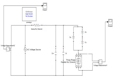
The calculated capacitance values are required to get desired partial discharge characteristics. Here an equivalent circuit of solid insulator having a cylindrical shape void is taken to evaluate the partial discharge characteristics. The Simulink model for detecting partial discharge characteristics is shown in figure 2.
Ca, Cb and Cc together constitutes test object. Where capacitor Cc represents capacitance of the void in the test object. Capacitor Cb represents capacitance of the healthy part connected in series with the void. Capacitor Ca represents the capacitance of the healthy part leaving Cc and Cb. Cm refers to the measuring capacitor and Ckrefers to the coupling capacitor.
The model drawn in Fig.2 is simulated using MATLAB. When high voltage is applied across the test object, voltage across the dielectric Va increases thereby the voltage Vc across the cavity also increases. When Vc reaches inception voltage, discharge in the void occurs. The voltage across the sample at which discharges begin to occur is called Inception voltage. In Fig 2 the partial discharge pulses in µv are seen in Scope2 which is connected through voltage measurement 1 across matching impedance. The applied input voltage is measured through voltage measurement 2 and witnessed in scope 1[5]. In this study the value of the HV equipment used for the measurement of PD inside the solid insulation is taken as depicted in table1.
Sl. No Parameter Symbol Value Dimension
1
HV measuring
capacitor
Cm 1000 pF
2 Coupling
capacitor Ck 1000 µF
3 Permittivity εo 8.85X10
-12 F/m
4 Relative
permittivity εr 3.5 -
5 Resistance R 50 Ω
6 Inductance L 0.60 mH
7 Capacitance C 0.45 µF
Table1: Parameters used for simulation
V. RESULT AND DISCUSSIONS
Charge Transfer:
Voltage across the void (Vc) is measured and applied to a subsystem in MATLAB simulink created as per the formula below.
Voltage across the cylindrical void Cc is given by
= × [3]
The apparent charge transferred is calculated by = ×
Fig 3: Variation of apparent charge for different radius (1mm to 20mm) of void keeping h constant(h=20mm) . It is observed from Fig 3 that, when the radius of void is varied from 1mm to 20mm charge has increased from 1.3907*10-15 C to 1.4125*10-11 C and the curve is slightly parabolic in nature.
Fig 4: Variation of apparent charge for different radius (1mm to 45 mm) of void keeping h constant(h=20mm) . It is observed from Fig 4 that, when the radius of void is varied from 1mm to 45mm the curve is parabolic up to 30mm. As the radius of the void is increased beyond 30mm the curve is linear and the rate of charge transfer is higher.
0 20 40 60 80 100 120 140
0 5 10 15 20
A p p ar en t ch ar ge i n 1 0 -1 3C o u lo m b s
radius in mm
0 200 400 600 800 1000 1200 1400 1600
0 10 20 30 40 50
A p p ar en t ch ar ge i n 1 0 -1 3C o u lo m b s
Radius of void in mm
0 2 4 6 8 10 12
0 5 10 15 20
A p p ar en t ch ar ge in 1 0 -1 3 C o u lo m b s
Height of void in mm
0 50 100 150 200 250 300 350 400 450 500
0 10 20 30 40
A p p ar en t ch ar ge in 1 0 -1 3 C o u lo m b s
Height of void in mm
Fig 5: Variation of apparent charge for different height (1mm to
20mm) of the void keeping r constant(r=10mm). Fig 6: Variation of apparent charge for different height (1mm to
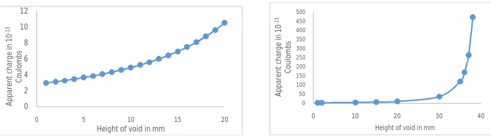
Figure 5, 6 shows the relation between apparent charge and variation in height of the void where the radius of the void is kept constant(r=10mm) at the applied voltage being 5kV.
It is observed from Fig 5 that, when the height of void is varied from 1mm to 20mm charge has increased from 8.8846*10 -13
C to 1.051*10-12C and the curve is slightly parabolic in nature. However, the observation from Fig 6 is that as the height of the void is increased beyond 30mm there is a rapid increase in charge transfer compared to the region where the height of the void is less than 30mm.
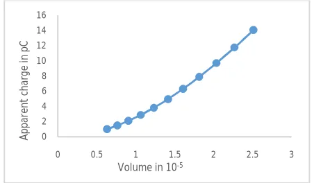
Fig 7: Variation of apparent charge for different volume of the void
Figure 7 shows relation between apparent charge and volume of the void. It is observed that the apparent charge transfer increases as the volume of void increases and the curve is almost linear.
The variations in the apparent charge transfer with respect to the dimensions of the void that isr, h and volume is as shown in figure 3, 4, 5 and 6.It is observed that as the applied voltage increases, the apparent charge transferred increases [6].
PD Amplitude:
Figure 8 and 9represents the variation of maximum PD amplitude in case of positive half cycle and negative half cycle of the applied voltage with respect to variation in r and h of the void. It is clear from the figures that the dimensions of the void affects the PD amplitude. It is also observed that the maximum amplitude of PD pulse increases in positive half cycle and decreases in negative half cycle as the dimension of the void varies.
0 2 4 6 8 10 12 14 16
0 0.5 1 1.5 2 2.5 3
A p p ar en t ch ar ge in p C
Volume in 10-5
0 2 4 6 8
1 2 3 4 5 6
M ax P D a m p lit u d e (µ V )
radius r in mm
Max PD amplitude in positive half cycle
Max PD amplitude in negative half cycle 0 1 2 3 4 5
2 3 4 5 6 7 8
M ax P D amp lit u d e( µ V )
Height in mm Max PD amplitude in positive half cycle
Max PD amplitude in negative half cycle
Fig 8: Variation of PD amplitude for different radius of the void
keeping h constant(h=20mm). Fig 9: Variation of PD amplitude for different height of the
Rise Time (tr) & Fall Time (tf):
The tr, tf and pulse width of the output pulses are calculated by considering six PD pulses, out of which three pulses are in positive half cycle and three pulses are in negative half cycle as shown in figure 10. Figure 10 represents the output PD pulses at 5 kV of applied voltage.
Fig 10: Output PD pulses at 5kV of applied voltage Fig 11: Rise time and fall time of PD pulse 2 in positive
The calculated rise time, fall time and pulse width of PD pulses considered in positive half cycle are depicted in Table 2. The tr and tf of pulse 2 is depicted in figure 11.The calculated rise time of the pulse 2 is 60µsec, the duration of rise time is between 6.35*10-3-6.41*10-3sec. The calculated fall time is 30µsec and duration of fall time is between 6.41*10-3-6.44*10 -3
. The pulse width of that pulse is the addition of rise time and fall time i.e. 90 microsecond.
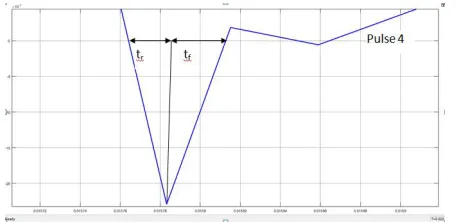
Fig 12: Rise time and fall time of PD pulse 4 in negative half cycle
The calculated rise time, fall time and pulse width of PD pulses considered in negative half cycle are depicted in Table 3.The tr and tf of pulse 4 is depicted in figure 12. The calculated rise time of the pulse 4 is 22µsec, the duration of rise time is between 0.01576-0.015782sec. The calculated fall time is 28µsec and duration of fall time is between 0.015782-0.01581sec. The pulse width of pulse 4 is addition of rise time and fall time i.e. 40 microsecond.
Table 2: Rise time (tr) and fall time (tf) of identified pulses at 5kV of applied voltage in positive half cycle. Pulse
no
Duration of rise time(sec) Rise time (µsec)
Duration of fall time(sec)
Fall time (µsec)
Total time (µsec)
1 3.51*10-3- 3.58*10-3 70 3.58*10-3-3.61*10-3 30 100
2 6.35*10-3-6.41*10-3 60 6.41*10-3-6.44*10-3 30 90
3 4.34*10-3-4.385*10-3 45 4.385*10-3-4.415*10-3 30 75
Table 3: Rise time (tr) and fall time (tf) of identified pulses at 5kV of applied voltage in negative half cycle. It is observed from the Table 2,3 that the PD pulses are having rise time, fall time and pulse width in the range of micro-second. The duration of the fall time is usually less than that of the rise time.
Variation of number of PDs with respect to phase angle:
Fig 13: Partial discharge pulses at different phase angle with different applied voltages in cylindrical void( r=10mmand height=20mm)
The partial discharge pulses are analyzed by dividing single applied sinusoidal cycle of 50 Hz into eight equal parts. Each part has 450 phase angle interval. The number of PD pulses for each interval is plotted for different applied voltages. Figures 13shows graph for number of PD pulses v/s different phase angle for different applied voltages (i.e, 5kV, 10kV and 15kV). The partial discharge phenomenon is random in nature so the numbers of PD pulses are not constant for every cycle [5].
Frequency content of obtained PD pulse:
Fig 14: Frequency plot of observed PD pulse at 5 kV applied Voltage.
0 5 10 15 20 25
0-45 46-90 91-135 136-180 181-225 226-270 271-315 316-360
N
o
. o
f
P
D
's
Phase angle 5kV 10kv 15kV Pulse
no
Duration of rise time(sec)
Rise time (µsec)
Duration of fall time(sec)
Fall time (µsec)
Total time (µsec)
4 0.01576-0.015782 22 0.015782-0.01581 28 40
5 0.01142-0.011485 65 0.011485-0.01152 35 100
Fast Fourier Transformation (FFT) is used to analyze the frequency content of the obtained PD pulse. The frequency plot of the observed PD pulse with applied voltage of 5 kV and dimension of the void is r=10mm, h=20mm is shown in figure14. PD phenomenon is random in nature. So, the frequency content of PD pulse is also fluctuating or random as the dimension of the void varies. It is also observed that the maximum amplitude of the frequency of the same PD pulse is appearing approximately around 4.5 kHz and 7.5 kHz which is shown in Fig.14. The dominant frequency of PD appeared because of the time duration of the PD pulses appears for such instance are much shorter compare to the other PD pulse instance present in the observed PD signal [3].
VI. CONCLUSION
Continuous monitoring of PD activity is essential to ensure the effective performance of the insulator. In this work, the effect of geometry of void present inside the insulation on the PD activity is analyzed. The variation of apparent charge transfer with variation in the dimensions (r, h and volume) of the void, PD amplitude with variation in the dimensions of the void is studied. When the radius of void from 1mm to 30mm with height being constant, the graph of apparent charge transfer with respect to radius and apparent charge transfer with respect to height from 1mm to 30mm with radius being constant is observed to be parabolic. As the radius of the void is increased beyond 30mm the curve is linear and the rate of charge transfer is higher. As the height of the void is increased beyond 30mm there is a rapid increase in charge transfer compared to the region where the height of the void is less than 30mm.The magnitude of internal discharges increases with increasing cavity dimensions. It is observed that the maximum amplitude of PD pulse increases in positive half cycle and decreases in negative half cycle as the dimension of the void varies. The PD activity depends upon the dimensions of the void. Rise time(tr), fall time(tf) and pulse width of the PD pulses are calculated. The PD pulses are having rise time, fall time and pulse width in the range of micro-second. The variation of number of PDs with respect to phase angle for different applied voltages is studied and it is random. The frequency content of PD pulse is analyzed and it is fluctuating as PD phenomenon is random in nature.
REFERENCES
[1] E.Kuffel, W.S.Zaengl and J.Kuffel, High voltage Engineering: fundamentals, second ed., Eleslever, 2005
[2] M.S.Naiduand V.Kamraju, High Voltage Engineering, NewDelhi: Tata McGraw- Hill,2004,pp.69-85.
[3] S.Karmakar and A.Sabat, “International Journal on Electrical Engineering and Informatics,” Simulation of Partial Discharge in High Voltage
Power Equipment,vol.3, nov.2,2011.
[4] F.H.Kreuger, Partial Discharge Detection in High-Voltage Equipment, London, United Kingdom: Butterworths &coLtd, 1989.
[5] C Sunil kumar, Dr. B. Ramachandra, “PD Analysis in Cubical Void With Respect to Geometry of the Void” International Journal of
Innovative Research in Electrical, Electronics, Instrumentation And Control Engineering vol. 4, issue 10, October 2016.
[6] R.Bartnikas, "Partial Discharge their mechanism, Detection and Measurement," IEEE Trans. Electr. Insul.,vol.9,pp. 763-808,2002
[7] C Sunil kumar, Dr. B. Ramachandra, Madhushree H N “Comparison of PD Activity in Cylindrical and Cubical Void using MATLAB
Simulink” International Journal of Innovative Research in Electrical, Electronics, Instrumentation And Control Engineering vol. 4, issue 10, October 2016
[8] C Sunil kumar, Harisha K S, Gouthami N, Harshitha V, Madhu C “Partial Discharge Analysis of a Solid Dielectric Using MATLAB
Simulink” International Journal of Innovative Research in Electrical, Electronics, Instrumentation And Control Engineering vol. 4, issue 6, June 2016.
[9] C. Smith, "Partial Discharge and Insulation failure," IPEC Ltd., 2005
[10] J. J. Smit, E. Gulski, P. Bauer, P. Cicheki and J. Setyawan, Investigation of Partial Discharge Occurrence and Detectability in High Voltage
Power Cable Accessories, Delft, 2009.
[11] R. J. Van Brunt, "Physics and Chemistry of partial discharges and corona," IEEE Trans. on dielectric and Electrical Insulation, vol. 1, no. 5,
pp. 761-784, 1994
BIOGRAPHY
C Sunil Kumar completed his Engg. from STJIT, Ranebennur and Masters from NIE Mysore, presently
Dr. B. Ramachandra working as Professor and Head in E&E Engg., PESCE, Mandya, Karnataka, India. He had his Ph.D from IISc. Bangalore, Master's from IIT-Bombay. He has about 25 scientific publications in this area. He is also academic active, guiding research students and interacting with universities.
H C Manohara completed his Engg. from SJCE, Mysore and Masters from SJCE, Mysore,