ANALYSIS OF FULL ADDER FOR POWER
EFFICIENT CIRCUIT DESIGN
Trapti Mittal
1, Uma Sharma
21
M.Tech, VLSI Design, 2Assistant Professor, ECE Deptt. AKGEC, (India)
ABSTRACT
MOS current mode logic (MCML) techniques are usually used for high-speed applications such as high speed
processors and multiplexers for optical transceivers. A new design of full adder is proposed based on MOS
Current Mode Logic (MCML). It is a new alternative for designing a full adder. Using MCML logic, the power
consumptions of circuits can be reduced to the effective level by supplying it with low power supply. The MCML
circuits are frequency independent circuits. Here, a 24 transistors full adder is constructed, a bias voltage Vb is
applied as the tail device works as a switch for design. The device is simulated using Tanner EDA tool V 14.0
with TSMC 180nm technology having voltage of 0.9V. By using same full adder, a 4-bit Ripple Carry Adder
(RCA) is also constructed.
Keywords:CMOS, Delay, Full Adder, MCML, Power Consumption.
I. INTRODUCTION
Digital circuit designers have always been encountered in a tradeoff between speed and power consumption to improve their design’s performance. There are standard implementations with various logic styles that have
been used in the past to design full-adder cells [16-38] and these are used for the comparison in this paper.
Although they all have similar function, the way of producing the intermediate nodes and the transistor count
are varied. Different logic styles tend to favor one performance aspect at the expense of the others. The logic
style used in logic gates basically influences the speed, size, power dissipation, and the wiring complexity of a
circuit. The circuit delay is determined by the number of inversion levels, the number of transistors in series, the
transistor sizes (i.e. channel widths) [1].
The MOS Current-Mode Logic (MCML) is a logic style which has gained an increasing popularity in several
applications. Indeed, compared to traditional CMOS logic, it exhibits a very low switching noise, a very high
speed and a better power efficiency at high operating frequencies other than a significantly lower sensitivity to
process variability. These features are exploited in current high resolution mixed signal Integrated Circuits
(ICs), high speed arithmetic cores, multiplexing/demultiplexing ICs for optical fiber communication systems
and RF circuits [2].
Static CMOS logic style is commonly used in the design of digital integrated circuits due to its advantages such
as very low static-power dissipation, high packing density and wide noise margins. However, this logic family is
highly susceptible to environmental noise sources such as electromagnetic coupling, power/ground noise, and
substrate noise; and its maximum operating frequency is orders of magnitudes less than fTof the MOS device. It
With the advancement of VLSI technology, many computing intensive applications such as multimedia
processing, digital communication can now be realized in hardware to either speed up the operation or reduce
the power/energy consumption. Transistor count is one of the major concerns, as it also leads to a reduction in
delay for the circuits. Two other important yet often conflicting design criteria are power consumption and
speed. A better metric would be the power delay product or energy consumption per operation to indicate the
optimal design tradeoffs.
Although dynamic power is continuously being reduced with technology scaling, static leakage power tends to
increase and is expected to become a large contributor to total power in a few technology generations [4].
There are three major components of power dissipation in complementary metal–oxide–semiconductor (CMOS)
circuits.
1) Switching Power: Power consumed by the circuit node capacitances during transistor switching.
2) Short Circuit Power: Power consumed because of the current flowing from power supply to ground during
transistor switching.
3) Static Power: Due to leakage and static currents.
As device density increases, it is also extremely desirable to integrate analog and digital circuitry onto the same
die for many DSP and communications systems. High levels of integration will be required in order to reduce
total system area and drive down production costs. This integration has been delayed due primarily to the
difficulty in designed high precision analog circuitry in the presence of extremely hostile digital switching noise.
These difficulties will also increase as process technology scales due to fundamental challenges in high
precision analog design at low supply voltages in digital CMOS technology. Either significant advances in
analog design techniques will be required or digital designers will be forced to adapt their design style or
process technology [5].
This paper deals with ripple carry full adders implemented in complementary metal oxide semiconductor
(CMOS) technology, which has the advantage of fractional voltage level at the internal nodes. A new full adder
is also proposed based on MCML technology with low power supply and can work for high speed applications.
II. CONVENTIONAL FULL ADDER REALIZATION
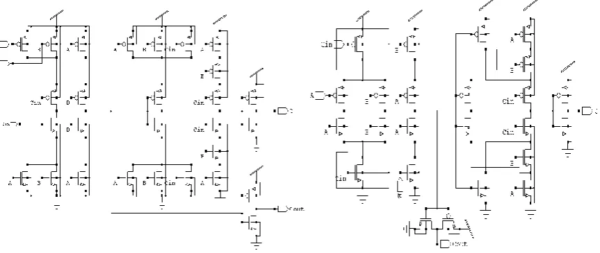
The 1-bit conventional CMOS full adder cell is shown in Fig. 1. The 1-bit full adder cell has 28 transistors. The
adder is implemented as a static CMOS logic circuit whose pull up (p channel) and pull down (n channel)
network have a mirror configuration with respect to the output nodes [6]. Every p channel transistor has its gate
connected to an n channel transistor to form a complementary pair. This solution has the following advantages:
The adder can be manufactured by a basic conventional CMOS process.
Using a mirror configuration makes it easier to design and optimize layouts, thus shortening the time to
market.
Using a mirror configuration reduces power consumption (to almost zero under the static conditions).
The transistor dimensions are easier to determine for a given manufacturing process.
On the other hand, conventional full adder implementation employs more transistors and cannot provide high
III. IMPROVED CONVENTIONAL FULL ADDER REALIZATION
An improvement is made in the original realization of conventional full adder with the aim of reducing the
transistor count. Its circuit diagram is shown in Fig. 3. Notice that the mirror approach isfollowed again. The
inverters for and are added for the purposes of this study the configuration of transistor shows the mirror
approach [7]. The following approach acquires less area on the area layout and because of the mirror image it
shows less difficulty. Recognized as an invention, the improved circuit configuration has these advantages:
It contains four transistors less than the conventional implementation, implying a saving in area.
The reduced number of interconnects means fewer parasitic resistors and capacitors, making for a higher
speed of operation.
The reduction in the number of circuit elements and interconnects should make the adder more reliable.
However, the carry transistors CIN and A–B ought to be connected differently relative to the power supply rail
and the output inverter, as indicated by the arrows in Fig. 2.
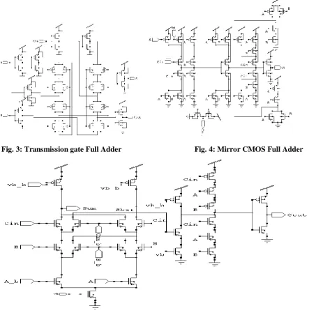
IV. TRANSMISSION GATE REALIZATION
Figure 3 gives a typical example of the transmission gate implementation. The circuit is designed for a 180 nm
CMOS process. Its advantages are as follows:
The transistor count can be reduced to 24.
Although the circuit in Fig.3 uses 30 transistors (as against 28 in the conventional version), in order to
achieve a higher speed, one can dispense with the inverters at the CIN and A inputs.
The adder offers a higher speed. The reason is that fewer logic gates have to be passed through by a signal as it
propagates from input to output; this also applies to the propagation of CIN, which determines the maximum
delay.
A disadvantage of the transmission gate implementation is increased power consumption, for a true and an
inverted signal cannot be generated simultaneously to drive the transmission gates. Note also that the presence
of cross coupling between the complementary transistors in the transmission gates poses a problem for layout
design [8].
V. MIROR CMOS FULL ADDER REALIZATION
Our implementation of a one bit full adder cell exploits the CMOS technology to reduce the maximum delay
through an n bit ripple carry full adder. A circuit diagram of the CMOS adder cell is shown in Fig.4.
With n bit ripple carry adders, the speed of operation is mainly limited by the time taken to generate and
propagate a carry from input to output in each one bit cell involved. The propagation delay is a function of the
total number of logic gates crossed. For given channel widths and lengths, the generation delay for each logic
gate varies with its output parasitic capacitances and the total channel resistance between each output node and
the power or ground line in a pull up or pulls down network. The output parasitic capacitance depends on how
With the above considerations in mind, we found a feasible way to reduce the capacitive load involved in
passing a carry from input to output, at the cost of increased capacitive load involved in sum generation.
This solution should enable one to construct n bit. Ripple carry full adders that would be superior in speed to the
alternative implementations if n > 3, as supported by computer simulations. It is protected by a patent.
VI. MOS CURRENT MODE LOGIC (MCML) BASED FULL ADDER REALIZATION
Here the author has proposed a 1-bit full adder cell consisting of 24 transistors multiplexers, called as MCML
based full adder design. The objective of using this method is to reduce the total power dissipation, time taken to
complete the operation and total power delay product. It also shows reduction in total number of transistor used.
The design is drawn in such a way that it generates the sum_bar signal too, with sum and carry signals. Here, the
half part is responsible for generating the sum signal and its complementary and other part generates the carry
signal [10].
MCML logic consists of bias voltage which works in triode region while working and other time remains off.
This bias voltage is applied at the tail of design and can be replaced with bias current and the resistance. This
tail voltage exactly works as a clock in domino logic design such as while the clock is conducting, it works only
for that duration, otherwise it is off. Due to this fact, it works with low power supply, consumes less power and
also this is a frequency independent design. It works best for high speed application [11].
For any digital design, three major sources of power dissipation are: short circuit current, leakage current and
logic transition. Here the short circuit is defined as the direct current passing from supply to ground, when
PMOS & NMOS transistors are active. As the given design is not directly connected to the supply and ground,
the short current will be negligible. To add to this, each transistor in the design is directly connected to the main
input so there will not be any delay, and shows the speed improvement in the circuit. Figure 5 shows the
schematic design. The simulation is carried out in Tanner EDA V 14.0 using TSMC 180 µm CMOS technology
at 0.9V supply and compared to other designs at frequency of 100MHz.
Fig. 3: Transmission gate Full Adder Fig. 4: Mirror CMOS Full Adder
Fig. 5 MCML Based Full Adder
V. SIMULATION AND RESULTS
For the comparison purpose with respect to power, delay and power delay product, these adders are simulated
using TANNER tool V14.0 TSMC180 nm in CMOS bulk technology with frequency of 100 MHz and supply
voltage of 0.9 V. the proposed MCML circuit shows less power consumption and less delay and lower power
delay product. The table 5.1 shows the comparison among the full adder designs for delay and power and The
TABLE 5.1
Implementation Delay, ns Power, µW Power delay Product,
pico unit
Transistor count
Cout SUM Cout SUM
Conventional
CMOS
1.855 2.592
8.739
16.210
22.592
28
Improved CMOS
1.960 2.698
8.732
17.115
23.558
24
Transmission
gate CMOS
3.723 1.832
1.75
6.515
3.206
32
Mirror CMOS
2.322 2.817
8.679
20.152
24.448
36
MCML based
CMOS
0.484 0.148
0.924
0.447
0. 137
24
Above table here shows the total power delay product and the total number of transistors used. From here, it can
clearly conclude that MCML based adder design takes less number of transistor and lower power delay product.
Table 5.3 shows the delay at sum outputs for each and every adder and shows the comparison, from here we can
drawn that MCML based RCA works faster than any other CMOS based RCA.
TABLE 5.2
Delay, ns
S0
S1
S2
S3
Conventional CMOS
1.215
0.797
0.529
1.017
Improved CMOS
1.327
0.759
0.539
0.713
Transmission gate CMOS
0.557
0.774
0.776
0.964
Mirror CMOS
0.5527
1.131
1.159
1.145
MCML based CMOS
0.488
0.412
0.475
0.346
VI. CONCLUSION
The above simulation and realization shows that for designing any digital circuit, MCML proves to be useful as
it takes less power and shows less power consumption. The MCML can be taken as a alternative to the CMOS
VII. ACKNOLEDGEMENT
I would like to extend my gratitude to Ajay Kumar Garg Engineering College, Ghaziabad that provides facilities
and resources in order to complete the research work. I also would like to thank my guide and friends.
REFERENCE
[1] R. Zimmermann and W. Fichtner, 1997, ―Low Power Logic Styles: CMOS Versus Pass-Transistor Logic,‖
IEEE J. Solid-State Circuits, Vol. 32, no. 7, pp. 1079–1089.
[2] H. Lee and G. E. Sobelman, 1997, ―A New Low Voltage Full Adder Circuit,‖ in IEEE proc. 7th great
lakes symosium vlsi, pp. 88–92.
[3] Ahmed M. Shams and Magdy A. Bayoumi, 2000, ―A Novel High Performance CMOS 1-Bit Full Adder
Cell,‖ IEEE transactions on circuits and systems—ii: analog and digital signal processing, Vol. 47, pp.
478-481.
[4] D. Radhakrishnan, 2001, ―Low Voltage Low Power CMOS Full Adder,‖ IEE proc. online no. 20010170
do1 io. 1049/ ip-cds: 20010170 IEE proc.-circuits devices system, Vol. 148, no. 1, pp 19-24.
[5] A. T. Schwarzbacher, J. P. Silvennoinen, and J. T. Timoney, 2002, ―Benchmarking CMOS Adder Structures,‖ in proc. ISSC, pp. 231–234.
[6] Yi Wei, Ji zhong Shen, 2011, ―Design of a Novel Low Power 8 Transistors 1 Bit Full Adder Cell,‖ journal
of zhejiang university-science c (computers & electronics) issn 1869-1951 (print); issn 1869-196x (online)
, pp. 604-607, www.zju.edu.cn/jzus, www.springerlink.com.
[7] V. V. Shubin, 2011, ―New CMOS Circuit Implementation of a One Bit Full Adder Cell,‖ ISSN 10637397,
russian microelectronics, Vol. 40, no. 2, pp. 119–127. © pleiades publishing, ltd.www.springerlink.com.
[8] Sohan Purohit, Martin Margala, 2012, ―Investigating the Impact of Logic and Circuit Implementation on Full Adder Performance,‖ IEEE transactions on very large scale integration (vlsi) systems, Vol. 20, no. 7,
pp. 1327-1321.
[9] D. V. Morozov, M. M. Pilipko, 2013, ―A Circuit Implementation of a Single Bit CMOS Adder,‖ ISSN
10637397, russian microelectronics, 2013, Vol. 42, no. 2, pp. 113–118. © pleiades publishing, ltd
www.springerlink.com.
[10] Hamid Reza Naghizadeh, Mohammad Sarvghad Moghadam, Saber Izadpanah Tous, Abbas Golmakani, 2013, ―Design of Two High Performance 1-Bit CMOS Full Adder Cells,‖ international journal of
computing and digital systems 2, no. 1, pp. 47-52.
[11] Yavuz Delican, Tülay Yildrim, 2011, ―High Performance 8-Bit MUX Based Multiplier Design Using MOS Current Mode Logic,‖ ELECO 2011 7th international conference on electrical and electronics
engineering Vol. 2, pp. 78-83.