Abstract—A compact ultra-wideband (UWB) antenna with tunable band notched characteristics is proposed. Varactor loaded, two via edge located (TVEL) and fractal electromagnetic band gap (EBG) structures are designed for tunable band-notched characteristics. The varactor diode near the TVEL EBG tunes the band-notch frequency for WiMAX (2.8–4.0 GHz) band, while another varactor near fractal EBG structure tunes band-notch frequency for WLAN (4.7–6.2 GHz) band. The varactors are independently controlled to achieve WiMAX and WLAN notched band. Notch frequencies can be continuously tuned by varying the bias voltage across the varactors. The proposed antenna of 24×24 mm2 dimensions is fabricated on an FR4 substrate. A good agreement between simulation and measurement results is obtained. A continuous band notch tuning from 2.8–4.0 GHz and 4.7–6.2 GHz is obtained using varactor diodes having capacitance in a range of 0.497–2.35 pF.
1. INTRODUCTION
UWB technology offers numerous advantages such as high data rate, low cost, low power consumption, and protection against multipath fading. UWB frequency range is assigned from 3.1 to 10.6 GHz by the Federal Communication Commission (FCC) [1]. UWB antennas of different shapes have been designed on different substrates [2–7]. Two half-elliptical shaped radiating elements fed by two Coplanar Waveguides (CPWs) are designed [2]. A miniaturized rectangular monopole antenna using electrically conductive adhesive on an FR4 substrate and carbon nanotube composite on Rogers 4350 are proposed in [3, 4]. A compact UWB antenna is printed on a 50.8-µm Kapton polyimide substrate [5]. A Vivaldi antenna with two pairs of eye-shaped slots is designed on an FR4 substrate to improve radiation characteristics in [6]. A metallic box-shaped antenna is designed for both narrow band and UWB in [7]. However, the designated UWB communication interferes with other narrowband systems, such as WiMAX (3.3–3.7 GHz), WLAN (5.1–5.8 GHz), and ITU satellite downlink communication (7.25–7.75). To avoid such potential interferences from these unwanted narrowband signals, band rejection features are required. In recent years, various design methods of UWB antenna with band-notch characteristic have been investigated [8–17]. Some conventional approaches carve differently shaped slots on radiating patches and adding stubs [8, 9], insertion of resonator structures such as split ring resonator (SRR), CSRR, and electric ring resonator (ERR) [10–12], using parasitic strips [13] and Electromagnetic Band Gap Structures (EBG) [14–17].
However, UWB antenna’s band-notched frequency [8–17] needs to be controlled and should be tunable to avoid fabrication errors and to meet the real-time reconfigurability. Thus, the reconfigurable technique has received considerable attention in wireless communications field. Therefore, it is necessary to design a tunable band-notch UWB antenna to adapt to an unstable environment. Several reconfigurable band-notched UWB antennas have been reported, and the frequency can be continuously tuned or reconfigurable by using a varactor diode, a PIN diode, and a capacitor [18–27]. In [18], a single
Received 18 August 2019, Accepted 6 November 2019, Scheduled 12 November 2019
* Corresponding author: Mahadu Annarao Trimukhe ([email protected]).
tunable band-notch frequency 4.62–5.83 GHz is achieved by using a varactor in a heart-shaped UWB antenna on a 30×40 mm2 substrate. Reconfigurable and tunable circular-shaped UWB antenna [19] is
designed on a 26×36.6 mm2 substrate. 4.2–4.8 GHz and 5.8–6.5 GHz bands are tuned by using varactor
diodes, and band-notch frequency is switched between 4.8 and 5.8 GHz bands by using a PIN diode. In [20], dual tunable band-notch frequencies 3.5–4.5 GHz and 5.3–6.05 GHz are achieved by using a varactor on a 34×27 mm2 substrate. A hexagonal-shape UWB antenna on a 30×30 mm2 substrate is designed, and tunable band notch frequencies are achieved by using varactor from 3.1–5.1 GHz and 7.25–9.9 GHz, respectively [21]. In [22], a CPW-fed UWB antenna on a 30×31 mm2 substrate has been reported, and tunable frequency from 3 to 4 GHz is achieved by using a capacitor. A flower-shape UWB antenna on a 42×50 mm2 substrate offers tunable band-notch frequency from 6.1 to 4.3 GHz by using a varactor and a capacitor [23]. A triangular-shaped UWB antenna [24], on a 40×30 mm2 substrate, offers tunable notch frequency at 5.3 and 3.4 GHz by using PIN diode and 5.57 and 3.52 GHz by using an ideal switch. A CPW-fed monopole antenna is switched to operate over WLAN and UWB using a capacitor in [25], while tunable and reconfigurable band notch antennas using capacitor are reported in [26, 27].
The antenna structures in [18–27], with single or dual tunable-band notched behavior employ a varactor, a PIN diode, and/or a capacitor. However, these antennas have large dimensions; some antennas cannot be tuned continuously and do not have appropriate tuned band notch capability.
A tunable band-notch UWB antenna is required to tune the band-notch frequency as the interfering bands differ slightly in different countries, to mitigate the variation in band notch due to fabrication error and to adapt to the unstable environment.
The proposed antenna is compact in size and tunes dual-band notched frequencies independently and continuously within UWB range by using varactor diodes. The radiation patterns are nearly omnidirectional.
2. DESIGN AND IMPLEMENTATION
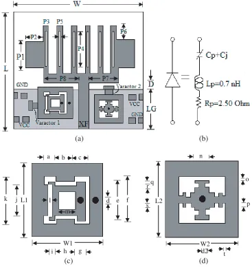
The configuration of the proposed antenna, equivalent circuit of varactor diode, and EBG structures with optimized parameters are shown in Figure 1. The structure is designed using multiple branches to resonate at different but nearby frequencies which electromagnetically couple to provide UWB. To reduce the size of the antenna, each branch is slotted. As a result, the effective current density at the edge of each branch increases, and path length increases. The antenna is designed on a 1.6 mm thick FR4 substrate with relative permittivity and loss tangent of 4.4 and 0.02, respectively. The structure is designed on an FR4 substrate to verify the design concept as it is easily available at low cost; however, high frequency performance of the structure degrades on FR4 substrate. The proposed structure on a low loss substrate exhibits similar band notch and improved radiation characteristics.
Optimized parameters of the antenna are L= 24, W = 24,P1 = 6, P2 = 2, P3 = 1.9, P4 = 6.6,
P5 = 0.4, P6 = 1.9,P7 = 5.6,P8 = 6.2,D= 2.2,XF = 3,LG= 7.6, P G= 0.30.
The parameters for TVEL-EBG are: W1 = 6, L1 = 6, a= 1, b = 1.6, c= 1.3, e = 3.2, f = 3.9,
g= 0.88,h= 1.84, i= 0.55,j= 2.5, k= 3.9,m= 1.38, l= 0.324, d= 0.78.
The parameters for fractal EBG are: W2 = 4.4, L2 = 4.8, n = 1, o = 0.2, p = 0.25, q = 0.3,
r= 0.25, s= 0.25,t= 0.25,d2 = 0.94 (all dimensions are in mm).
A compact UWB antenna with triple band-notch characteristics using two EBG structures is proposed by the authors in [28]. A single TVEL-EBG structure is used to achieve WiMAX and satellite downlink band notch, while a fractal EBG structure is used to obtain WLAN band notch. The proposed TVEL EBG structure has one via in the outer metallic ring and another via to inner metallic ring. Outer metallic ring with via and the gap between the two metallic rings determine the WiMAX band-notch frequency. The dimensions of the inner metallic ring determine the satellite downlink band-notch frequency.
EBG structures act as a parallel LC circuit, and the current flowing through via and ground plane results in an inductor L, whereas the gap between the adjacent EBG units results in capacitance C. The values of L in Henry andC in Farad are approximately given [29].
a b c
e d
i h g
W1 L1 j k f m l a s q r t d2 W2
L2 p
o n
(a) (b)
(c) (d)
Figure 1. (a) Compact tunable UWB antenna. (b) Equivalent circuit of the varactor diode (Cp = 0.44 pF, Cj = 0.497–2.35 pF). (c) Geometry of the TVEL EBG structure. (d) Geometry of the fractal EBG structure.
whereμ0 = permeability of free space,h= substrate height and
C = ω1ε0(εr+ 1)
π cos
−1
2ω1+pg
pg
(2)
where ω1 is the width of the EBG metal patch; PG is the gap between two EBG cell; ε0 and εr
are the permittivity of air and relative permittivity of the substrate, respectively. Bandgap BW is approximately determined by [29].
BW = Δω
ω (3)
Equivalent L-C circuits of TVEL and Fractal EBG are shown in Figures 2(a) and (b), respectively. In TVEL EBG, capacitance C1 is predominant due to outer slot. L1 is due to the current flowing in
via close to feed line and outer rectangular metallic ring. The nonuniform width of outer slot helps in achieving wideband notch. C3 is due to inner slot, and inductanceL3 is due to current flowing in inner
via and inner rectangular metallic strip. In fractal EBG, C2 is due to slots, and L2 is due to current
L1
C1 C3
L3
C2
L2
(a) (b)
Figure 2. Equivalent circuits. (a) TVEL EBG. (b) Fractal EBG.
and fractal EBG structures can be given as [28].
fci= 1
2π√LiCi (4)
Here i= 1, 3 is for TVLE andi= 2 fractal EBG structures.
The authors have explained the design process of the proposed EBG structures in [28].
To achieve a variable notch frequency, we need to change the effective electrical length of the EBGs. Therefore, a varactor diode (Skyworks SMV1231) with capacitance range from 0.497 pF to 2.35 pF is placed in series with the EBG structures as shown in Figure 1(a). To achieve tunability over WiMAX and WLAN band, the diodes are located near the TVEL and fractal EBG structure, where the surface current density is maximum. By varying the capacitance of the varactor diodes, the electrical length of EBG and therefore, the central frequencies of the notched band are varied. Figure 1(b) shows the series RLC equivalent circuit model of a varactor diode, and it contains a parasitic inductance of diode Lp
(0.7 nH), a series resistanceRp (2.5 Ω), and total capacitance which consists of parasitic capacitanceCp
(0.44 pF) and junction capacitance Cj, according to the spice model. Since a reverse DC bias voltage (10 V–0 V) is required to achieve tuning of the diode corresponding to the junction capacitance (Cj) in the range of 0.497–2.35 pF, a bias circuit is required to isolate the parasitic effects of the voltage supply. DC bias voltage is isolated from RF signal with the help of an RF chock coil of 33 nH in the bias circuit. Also, the gap between EBG structures and feed line acts as a DC blocking capacitor. Therefore, DC biasing circuit does not affect the RF performance of radiator.
3. SIMULATED AND MEASURED RESULTS
Antenna structures are simulated and optimized using High-Frequency Structures Simulator (HFSS) software. Figure 3 shows the simulated surface current distribution of the proposed antenna when the varactor diode junction capacitance is 0.613 pF (6 V). At operating frequency of 4.0 GHz, the surface current distribution on the EBG structures is quite little, as evident from Figure 3(a). The surface current is mainly concentrated on the edge of the patch and the feed line which indicates that the EBG structures, at operating frequency, have little effect on the performance of UWB antenna. At the central band-notch frequencies, in this case at 3.3 GHz and 5.3 GHz, most of the surface current is concentrated on the TVEL EBG and fractal EBG, respectively. Figures 3(b) and (c) indicate that that the TVEL EBG and fractal EBG resonate near 3.3 GHz and 5.3 GHz, respectively, and as a result, the antenna becomes non-responsive and therefore does not radiate effectively and forms a dual notched band antenna. The structure behaves similarly at other bias voltages. When the surface current distributions are less under particular dc bias, it implies that this bias circuit has little effect on the performance of the antenna.
(a) (b)
(c)
Figure 3. Surface current distribution at the frequency of (a) 4.0 GHz, (b) 3.3 GHz, (c) 5.3 GHz.
(a) (b)
Figure 4. Photograph of the fabricated antenna: (a) top view; (b) bottom view.
voltage. The second varactor D2 is integrated to a fractal EBG structure; therefore, it affects WLAN band notch independently.
(a) (b)
Figure 5. (a) Simulated VSWR for different capacitances of varactor diode 1, (b) VSWR for WiMAX tunable band.
(a) (b)
Figure 6. (a) Simulated VSWR for different capacitances varactor diode 2, (b) VSWR for WLAN tunable band.
gets added in series to the distributed capacitance of the EBG structures. By varying the junction capacitance Cj of the two varactor diodes from 2.35–0.497 pF (or increasing the varactor diode biases from (0–10 V), the central frequency is tuned from 2.8–4.0 GHz and 4.7–6.2 GHz, respectively.
The simulated and measured VSWRs, for DC bias voltage 0 V to 10 V in step of 2 V applied to varactor diodes D1 and D2, are shown in Figure 8. The simulated results agree with measured ones. The discrepancy may be attributed to connector loading, error in fabrication, DC bias, etc. Frequency shifts of central notch frequency with respect to 0 V DC bias voltage for both the notch bands are shown in Figure 9. CT of varactor diode depends on reverse bias voltage, and it decreases nonlinearly with increase in reverse bias voltage. Therefore, increase in the capacitance of EBG structure due to varactor diode and frequency decreases nonlinearly with increase in DC reverse bias voltage.
The simulated and measured radiation performance characteristics are investigated for three cases:
(a)
(b) (c)
Figure 7. (a) Simulated VSWR of the proposed antenna for both varactor different capacitances. (b) Tunable WiMAX band (2.8–4.0 GHz). (c) Tunable WLAN band (4.7–6.2 GHz).
(< 1.2 dBi), and antenna efficiency is more than 60% (> 58%) over UWB. The simulated (measured) gain and efficiency decrease significantly at the triple band-notched frequencies, i.e., around 3.8 GHz (3.7 GHz), 5.5 GHz (5.4 GHz), and 7.5 GHz (7.515 GHz). The band-notch tuning for different DC bias voltages can be visualized from antenna gain and efficiency plots shown in Figure 10. The gain and efficiency minima, for WiMAX band notch, shift from 3.8 GHz at 0 V to 3.2 GHz at 2 V and to 3.1 GHz at 6 V. For WLAN band notch, it shifts from 5.5 GHz at 0 V to 5.2 GHz at 2 V, and 5.0 GHz at 6 V. The gain variation is <1.2 dBi over UWB, and antenna efficiency is >58% for both DC bias voltages except at notched bands of 3.1 GHz and 5.1 GHz, where the antenna efficiency decreases to 18% and 20%, respectively.
higher-(a) (b)
(c) (d)
(e) (f)
Figure 8. Simulated and measured VSWR of the proposed antenna at different DC bias voltages.
(a) (b)
Figure 9. Frequency shift of central band notch frequency vs. DC bias voltage with respect to the 0 V, (a) WiMAX, (b) WLAN band notch.
(a) (b)
(e) (f)
Figure 10. Gain and efficiency of proposed antenna for three different DC bias voltages.
(a) (b)
(e) (f)
Figure 11. Comparison of measured and simulated radiation patterns of proposed antenna: (a), (c) and (e)E-plane, (b), (d) and (f) H-plane.
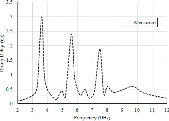
Figure 12. Measured group delay of the proposed antenna.
Another key element of UWB performance of the antenna is group delay. The group delay of the proposed antenna is measured between transmitter and receiver antennas facing each other and placed at a distance of 20 cm in broad side direction. The measured group delay is shown in Figure 12. The group delay varies from 0.1 to 0.6 ns in passband. This small variation in the group delay implies that the designed antenna exhibits good phase linearity at entire UWB except at notched band.
Table 1. Comparison of proposed antenna with other state of art band notch tunable UWB antenna.
Ref. Size (mm2) εr/h(mm) Tunable/Reconfigurable method
Tunable/Switchable Freq. Range (GHz)
[18] 30×40 2.2/0.508 Varactor 4.62–5.83
[19] 26×36.6 4.4/1 Varactor 4.2–4.8/5.8–6.5
[20] 34×27 2.2/0.787 Varactor 3.5–4.5/5.3–6.05
[21] 30×30 4.4/0.8 Varactor 3.1–5.5/7.25–9.9
[22] 30×31 3.38/1.5 Capacitor 3.0–4.0
[23] 42×50 4.5/1.6 Varactor/Capacitor 6.1 and 4.3
[24] 40×30 2.2/0.787 PIN/Ideal Switch 5.3 and 3.4/5.57 and 3.52
[25] 24×30.5 3.38/1.5 Capacitor 5.0–6.0/3.1–10.6
[26] 24×30.5 3.38/1.5 Capacitor 5.5/3.0–11.0
[27] 24×30.5 3.38/1.5 Capacitor 3.1–2.9/7.0–5.8
Proposed 24×24 4.4/1.6 Varactor 2.8–4.0/4.7–6.2
4. CONCLUSION
In this paper, a compact UWB antenna with tunable dual band-notched characteristics is proposed. Varactor diodes integrated to TVEL and fractal EBG are independently controlled to tune WiMAX and WLAN band notch frequencies. A continuous band-notch tuning from 2.8–4.0 GHz and 4.7–6.2 GHz is obtained. The proposed antenna has a nearly omnidirectional radiation pattern suitable for short range UWB wireless application.
REFERENCES
1. Anon, “FCC first report and order on ultra-wideband technology,” FCC 802 Standards Notes, Feb. 2002.
2. Raad, H. K., “An UWB antenna array for flexible IoT wireless systems,” Progress In Electromagnetics Research, Vol. 162, 109–121, 2018.
3. Reyes-Vera, E., M. Arias-Correa, A. Giraldo-Muno, D. Catano-Ochoa, and J. Santa-Marin, “Development of an improved response ultra-wideband antenna based on conductive adhesive of carbon composite,” Progress In Electromagnetics Research C, Vol. 79, 199–208, 2017.
4. Mehdipour, A., I. D. Rosca, A.-R. Seba, C. W. Trueman, and S. V. Hoa, “Carbon nanotube composites for wideband millimeter-wave antenna applications,” IEEE Transactions on Antennas and Propagation, Vol. 59, No. 10, 3572–3578, 2011.
5. Khaleel, H. R., H. M. Al-Rizzo, D. Rucker, and S. Mohan, “A compact polyimide-based UWB antenna for flexible electronics,”IEEE Antennas and Wireless Propagation, Vol. 11, 564–567, 2012. 6. Ma, K., Z. Zhao, J. Wu, S. M. Ellis, and Z.-P. Nie, “A printed Vivaldi antenna with improved radiation patterns by using two pairs of eye-shaped slots for UWB applications,” Progress In Electromagnetics Research, Vol. 148, 63–71, 2014.
7. Zivkovic, I. and K. Scheffer, “A new innovative antenna concept for both narrow band and UWB applications,” Progress In Electromagnetics Research, Vol. 139, 121–131, 2013.
8. Hosseini, H., H. R. Hassani, and M. H. Amini, “Miniaturised multiple notched omnidirectional UWB monopole antenna,”Electronics Letters, Vol. 54, 472–474, 2018.
“Miniaturised UWB antenna with dual-band rejection of WLAN/WiMAX using slitted EBG structure,” IET Microwaves, Antennas &Propagation, Vol. 13, No. 3, 360–366, 2019.
15. Bhavarthe, P., S. Rathod, and K. T. V. Reddy, “A compact dual band electromagnetic band gap structure,” IEEE Transactions on Antennas and Propagation, Vol. 67, No. 1, 596–600, 2019. 16. Jaglan, N., S. D. Gupta, B. K. Kanaujia, and S. Srivastava, “Band notched UWB circular
monopole antenna with inductance enhanced modified mushroom EBG structures,” Wireless Personal Communications, Vol. 24, No. 2, 383–393, 2018.
17. Peng, L. and C.-L. Ruan, “UWB band-notched monopole antenna design using electromagnetic-bandgap structures,” IEEE Transactions on Microwave Theory and Techniques, Vol. 59, No. 4, 1074–1081, 2011.
18. Hua, C., Y. Lu, and T. Liu, “UWB heart-shaped planar monopole antenna with a reconfigurable notched band,”Progress In Electromagnetics Research Letters, Vol. 65, 123–130, 2017.
19. Wu, W., Y.-B. Li, R.-Y. Wu, C.-B. Shi, and T.-J. Cui, “Band-notched UWB antenna with switchable and tunable performance,” International Journal of Antennas and Propagation, Vol. 2016, 1–6, 2016.
20. Tang, M.-C., H. Wang, T. Deng, and R. W. Ziolkowski, “Compact planar ultra-wideband antennas with continuously tunable, independent band-notched filters,” IEEE Transactions on Antennas and Propagation, Vol. 64, No. 8, 3292–3301, 2016.
21. Elfergani, I., J. Rodriguez, I. Otung, W. Mshwat, and R. Abd-Alhameed, “Slotted printed monopole UWB antennas with tunable rejection bands for WLAN/WiMAX and X-band coexistence,”
Electromagnetics, Vol. 27, No. 3, 694–702, 2018.
22. Nejatijahromi, M., M. Rahman, and M. Naghshvarianjahromi, “Continuously tunable WiMAX band-notched UWB antenna with fixed WLAN notched band,” Progress In Electromagnetics Research Letters, Vol. 75, 97–103, 2018.
23. Mohamed, H. A. E., A. S. Elkorany, S. A. Saad, and D. A. Saleeb, “New simple flower shaped reconfigurable band-notched UWB antenna using single varactor diode,” Progress In Electromagnetics Research C, Vol. 76, 197–206, 2017.
24. Alhegazi, A., Z. Zakaria, N. A. Shairi, I. M. Ibrahim, and S. Ahmed, “A novel reconfigurable UWB filtering-antenna with dual sharp band notches using double split ring resonators,” Progress In Electromagnetics Research C, Vol. 79, 185–198, 2017.
25. Nejatijahromi, M., M. Naghshvarianjahromi, and M. Rahman, “Switchable planar monopole antenna between ultra-wideband and narrow band behavior,” Progress In Electromagnetics Research Letters, Vol. 75, 131–137, 2018.
26. Jahrom, M. N., M. N. Jahrom, and M. U. Rahma, “A new compact planar antenna for switching between UWB, narrow band and UWB with tunable-notch behaviors for UWB and WLAN application,”ACES Journal, Vol. 3, No. 4, 400–406, 2018.
28. Trimukhe, M. A. and B. G. Hogade, “Compact ultra-wideband antenna with triple band notch characteristics using EBG structures,” Progress In Electromagnetic Research C, Vol. 93, 65–77, 2019.
29. Yang, F. and Y. Rahmat-Samii, “Microstrip antennas integrated with electromagnetic band-gap (EBG) structures: A low mutual coupling design for array applications,” IEEE Transactions on Antennas and Propagation, Vol. 51, No. 10, 2936–2946, 2003.