Design of Level Shifter with Wide Input Voltage Range
P Pydi Reddy & Dr. M Ashok Kumar
M.Tech Student[1], Associate Professor[2]
Pydah College of Engineering and Technology [1,2]
Abstract—The level shifters are crucial primitives in the multi supply voltage circuits and systems. In this project, a level shifter is proposed to achieve the conversion from the sub-threshold voltage to the above threshold voltage for different input voltages. It is a hybrid structure consisting of the Wilson current mirror and cross- coupled level shifter. By addressing the voltage drop issue of the level shifter based on the Wilson current mirror, the leakage power is significantly reduced, with the advantage of wide input voltage range for the Wilson current mirror level shifter well preserved. In addition, the multi-threshold CMOS (MTCMOS) technology is employed to provide more flexibility for our ultra-low power design. The reporter simulation results using 65nm CMOS process validate our proposed implementation and an ultra-low power consumption of 5.6 uJ per conversion from 0.09 V to 1.2 V at 1MHz is achieved without the need of any intermediate power supply.
I. INTRODUCTION
In the last few decades due to the ever-growing demand for portable and small sized devices, integrated circuits require electronic circuit design methods to implement integrated circuits with low power consumption. The ever-growing number of transistors integrated on a chip and the increasing transistor switching speed in recent decades has enabled great performance improvement in computer systems by several orders of magnitude. Unfortunately, such phenomenal performance improvements have been accompanied by an increase in power and energy dissipation of the system.
The ever-growing number of transistors integrated on a chip and the increasing transistor switching speed in recent decades has enabled great performance improvement in computer systems by several orders of magnitude. As the scale of integration of the components keeps on growing, more and more
sophisticated on the silicon wafer most of the applications not only demanding for computation capacity but also consuming the considerable amount of energy. Performance and area are two major design goals, with power consumption being a critical concern in today’s VLSI system design. The need for low power VLSI system leads to two main forces. First, with the steady growth of processing capacity per chip, large current has to deliver and the heat due to large power consumption must be removed by proper cooling techniques. Second, battery life in portable electronic devices is limited. Low power design is mostly needed in these portable devices. Also, with shrinking technology sizes, energy efficiency has become a critical aspect of designing digital circuits. Traditionally, voltage scaling, a mechanism in which the supply voltage is varying and the threshold voltage is constant, has been an effective solution in meeting stringent energy requirements. However, voltage scaling does come at a cost of reduction in performance. The limits of voltage scaling, and therefore energy minimization, can be explored by operating a circuit at sub threshold. In sub threshold circuits, the supply voltage is reduced well below the threshold voltage of a transistor. Due to the quadratic reduction in power with respect to the supply voltage, sub threshold circuits are classified as ultra low power circuit. For the design of low power devices where performance can be sacrificed, sub- threshold circuits are an ideal method for designing. Some of the applications include devices such as digital wrist watches, radio frequency identification, sensor nodes, pacemakers and battery operated devices such as, cellular phones.
The design concern on maximizing the performance while minimizing the power consumption has become more and more critical not only in the mobile consumer electronics but also in the wired embedded systems and high-end computing platforms [1], [2]. In [1], multi-supply-voltage implementation has been proven an effective solution to lower the power consumption, and the implementation capable of near-threshold and sub-threshold operations have been proposed to provide optimal energy consumption [2]. However, sufficient driving strength for large capacitance of the interfaces or IO pads requires normal supply voltage for the related transistors (e.g. 1.8 V). Therefore, the level shifters are always inevitable for the conversion between different voltages.
In the past few years, a number of level shifter implementations have been proposed [3]–[7]. Most of them are based on two conventional designs: the cross-coupled structure and the current mirror structure [8]. Fig. 1 shows the schematics of the two designs. It is disclosed that both of them employ a differential input generated by an inverter stage. The cross- coupled level shifter in Fig. 1 (a) takes
significant advantage of the full output swing generated by a positive feedback. The major limiting issue for this design is that the driving strength for the NMOS pair (MN1 and MN2) is much weaker than that of the PMOS pair, when the input is below the threshold voltage of the NMOS pair. This result in the failure of the output’s toggling. Although the driving strength can be improved by greatly upsizing the NMOS pair, it is at the cost of large area and load capacitance. Fig. 1 (b) shows a topology that uses a current mirror to level shift before the output buffer. However, the static current flowing through MP1 and MN1 consumes large static power when the input is high. To reduce this static current, the Wilson current mirror based level shifter was proposed in [3] (Fig. 2), which adds a feedback PMOS (MP3) to reduce the static current. However, before the output buffer, the feedback by MP3 introduces a voltage drop (i.e. Vgs of MP3) below VDDH, which can cause large static current in the buffer. The voltage drop can be reduced by upsizing MP3, nevertheless, it can result in increment of both the delay and power consumption for the high-to-low transition.
In this paper, we present an energy-efficient level shifter with a wide input voltage range. It is a hybrid structure of the Wilson current mirror based level shifter and the conventional cross-coupled level shifter. By addressing the voltage drop issue of the level shifter based on the Wilson current mirror, the leakage power is significantly reduced, while the advantage of wide input voltage range for the Wilson current mirror level shifter is well-preserved. Specifically, the voltage drop of the Wilson
any intermediate power supply. The rest of the paper is organized as follows. In Section II, the implementation of the proposed level shifter is
elaborated. The simulation results are presented and discussed in Section III. Finally, the conclusion is drawn in Section IV.
III. PROPOSED LEVEL SHIFTER
IMPLEMENTATION
Fig. 3 shows the VLSI implementation of the proposed level shifter. The MTCMOS technique is employed in the design to optimize the delay and the power consumption. The proposed level shifter mainly consists of two Wilson current mirrors as its initial level-up stage, and a cross coupled structure as its output stage. The differential inputs are generated by an inverter with low threshold voltage Vth, featuring a shorter delay. Moreover, the Wilson current mirrors raise the input voltage to a voltage near or above the threshold of the
NMOS. In order to reduce the power consumption, the lengths of PMOS transistors in the current mirror are larger than the process feature size. The W/L ratios of the output transistors MP2, MN2, MP5 and MN4 for the current mirror can be increased, in order to achieve a higher speed. The full swing of the output is maintained by the following cross coupled structure, and the pull-down strength is improved by using low Vth NMOS for MN5 and MN6, while the active current is limited by using high Vth PMOS for MP7 and MP8.
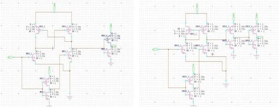
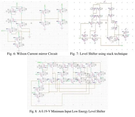
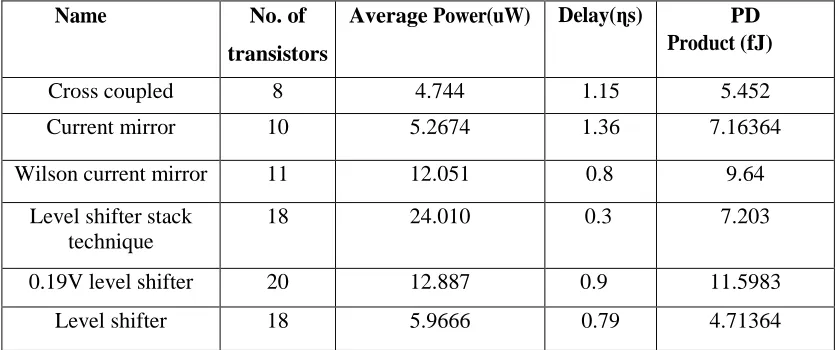
The schematics of the circuits that were designed are shown below.
Fig. 6: Wilson Current mirror Circuit Fig. 7: Level Shifter using stack technique
Fig. 8: A 0.19-V Minimum Input Low Energy Level Shifter
Fig. 9: Proposed Level Shifter
The schematics drawn in tanner tools are shown below along with the simulated waveforms obtained using Avan waves in H-spice simulation.
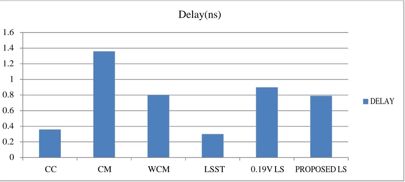
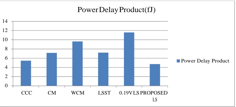
Table 1Summarizes the circuit features and the simulation results. For circuit features, although the proposed design does not use the least number of transistors, it has the smallest layout area
Table 1
Name No. of
transistors
Average Power(uW) Delay(ɳs) PD Product (fJ)
Cross coupled 8 4.744 1.15 5.452
Current mirror 10 5.2674 1.36 7.16364
Wilson current mirror 11 12.051 0.8 9.64
Level shifter stack technique
18 24.010 0.3 7.203
0.19V level shifter 20 12.887 0.9 11.5983
Level shifter 18 5.9666 0.79 4.71364
The graph below shows the average power consumed by the 6 compared designs and the proposed design Level Shifter are compared and it is clear that the power consumption of level
Fig. 10: Average power consumed by various designs
The delay for the designs cross coupled, current mirror, Wilson current mirror, level shifter stack technique, 0.19v low power level shifter and the proposed design Level Shifter are calculated and the bar graph is plotted. From the below figure it can be
inferred as Level Shifter using stack technique has the least delay but has the highest power consumption and hence the highest power delay product.
Fig. 11: Delay Produced by Various Designs Delay(ns)
1.6
1.4
1.2
1
0.8
0.6
0.4
0.2
0
DELAY
CC CM WCM LSST 0.19V LS PROPOSED LS
Average Power(uW
)
30
25
20
15
Average Power
10
5
0
We have seen that cross coupled has less power but disadvantage in it is, it has less input driving capability. Current mirror has less power but the
power delay product is high. On comparing overall designs the proposed level shifter has the least power delay product.
Fig. 12: Power Delay Product of Various Level Shifters Furthermore, the concern of process variation
has become more and more significant for the sub threshold analog circuit design. The robustness of the proposed level shifter against the process variations has been verified with extensive Monte Carlo simulations, where 100 runs of transistor-level Monte Carlo simulation have been performed for the voltage conversion from 0.09 V to 1V. Both switches of the inter-die and intra-inter-die process variations are turned-on in the simulation
V. CONCLUSION
In this project an energy-efficient sub threshold level shifter is designed. The implemented hybrid structure combining the Wilson current mirror and cross-coupled level shifter takes the advantages while overcomes the drawbacks of the two structures. In addition, MTCMOS devices are applied to achieve low power/energy consumption. The simulation results using 65 nm CMOS technology show it only consumes 5.966uW average power for 0.09 V to 1.2V conversion at an operating frequency of 1 MHz, with the input high voltage level as
low as 400 mV. In this project we designed and implemented the circuit using 65nm technology by using 18 transistors. The present level shifter consumes less power compared to previous systems. In future, it can be extended further by using transistors less than the present circuit transistors. And also to design the circuit which can operate at high frequency by scaling the transistor size very low by using technology files like 45nm, 28nm, 22nm, 14nm. This energy-efficient level shifter with a wide input range can find applications in the interfaces between sub threshold and above threshold voltage modules. The application composed of storage of lower voltage output of multiplexer into the static random access memory (SRAM) operating at higher supply voltage. Multiplexer is operating at supply voltage of 0.09-V, while SRAM is operating at supply voltage of 1-V. Thus, to provide the output of multiplexer to SRAM, voltage level shifter is used in between them. The output of multiplexer is given to voltage level shifter, which up-converts this output to 1-V from 0.09-V. Then, 1.2-V output of voltage level shifter is provided as input to SRAM. This 1.2-V output is then stored in the
Power Delay Product(fJ)
14
12
10
8
6
4
2
0
Power Delay Product
CCC CM WCM LSST 0.19V LS PROPOSED
SRAM.
REFERENCES
[1] J. C. Chi, H. H. Lee, S. H. Tsai, and M. C. Chi, “Gate level multiple supply voltage assignment algorithm for power optimization under timing constraint,” IEEE Trans. Very Large Scale Integr. (VLSI) Syst., vol. 15, no. 6, pp. 637–648, June 2007.
[2] H. Fuketa, M. Nomura, M. Takamiya, and T. Sakurai, “Intermittent resonant clocking enabling power reduction at any clock frequency for
near/sub-threshold logic circuits,” IEEE Journal of Solid-State Circuits, vol. 49, no. 2, pp. 535– 544, Jan. 2013.
[3] S. Lutkemeier et al., “A subthreshold to above-threshold level shifter comprising a Wilson current-mirror,” IEEE Trans. Circuits Sys. II Exp
Briefs, vol. 57, no. 9, pp. 290–294, Sept. 2010. [4] Y. Osaki, T. Hirose, N. Kuroki, and M. Numa, “A low-power level shifter with logic error correction for extremely low-voltage digital CMOS
LSIs,” IEEE Journal of Solid-State Circuits, vol. 47, no. 7, pp. 1776– 1783, July 2012.
[5] S.-C. Luo, C.-J. Huang, and Y.-H. Chu, “A wide-range level shifter using a modified wilson current mirror hybrid buffer,” IEEE Trans. Circuits Sys.I Regular Papers, vol. 61, no. 6, pp. 1656–1665, May 2014.
[6] R. Matsuzuka, T. Hirose, Y. Shizuku, N. Kuroki, and M. Numa, “A 0.19- V minimum input low energy level shifter for extremely low-voltage VLSIs,” in Proc. 2015 IEEE International Symposium on Circuits and Systems (ISCAS), Lisbon, May 2015, pp. 2948– 2951.
[7] S. Hosseini, M. Saberi, and R. Lotfi, “An energy-efficient level shifter for low-power applications,” in Proc. 2015 IEEE International Symposium on Circuits and Systems (ISCAS), Lisbon, May 2015, pp. 2241–2244.
[8] K.-H. Koo, J.-H. Seo, M.-L. Ko, and J.-W. Kim, “A new level-up shifter for high speed and
wide range interface in ultra deep sub-micron,” in