ABSTRACT
CASTRO, SUSANA PATRICIA. Characterization of the Boron Doping Process Using Boron Nitride Solid Source Diffusion
The purpose of this research has been to develop an optimum process for the boron
doping of implants and polysilicon gates of metal-oxide-semiconductor (MOS) devices.
An experimental design was constructed to determine the effects of diffusion
temperature, time, and ambient on characteristics of the doping process. A temperature
range of 800 to 1000 degrees Celsius was studied with a diffusion time between 10 and
60 minutes. Two diffusion ambients were used for doping processes, a pure nitrogen
ambient and a nitrogen-oxygen gaseous mixture. Device wafers were fabricated, and the
testing of MOS capacitors and van der Pauw test structures was performed to determine
the effect of diffusion conditions on flatband voltage and poly gate doping. Materials
characterization techniques were used on monitor wafers for each diffusion process to
determine the wafer structure formed for each process and evaluate the effectiveness of
the deglaze etch. The processes that resulted in the best device characteristics without
suffering from significant poly depletion effects and flatband voltage shifts were wafers
doped at 800 degrees Celsius in a pure nitrogen atmosphere for 20 minutes and 45
minutes. The presence of oxygen in the atmosphere caused the depletion of boron from
the Si wafer surface. The formation of the Si-B phase only occurred on devices processed
at 1000 degrees Celsius. The deglaze process used in this experiment did not fully
CHARACTERIZATION OF THE BORON DOPING PROCESS USING BORON NITRIDE SOLID SOURCE DIFFUSION
by
SUSANA PATRICIA CASTRO
A thesis submitted to the Graduate Faculty of North Carolina State University
in partial fulfillment of the requirements for the Degree of
Master of Science
MATERIALS SCIENCE AND ENGINEERING
Raleigh
1999
APPROVED BY:
________________________________ ________________________________
PERSONAL BIOGRAPHY SUSANA P. CASTRO
Susana P. Castro was born in the capital city of Honduras, Tegucigalpa. Because of
her father’s occupation at the United States Agency for International Development
(USAID), she lived her childhood and adolescent years in several countries, including the
United States of America, the Dominican Republic, and Guatemala. She spent more than
half of her life in northern Virginia, where she completed her high school education. She
graduated from Virginia Polytechnic Institute and State University in May of 1997 with a
B.S. in Materials Science and Engineering. Her most treasured experiences in the field of
engineering took place throughout her undergraduate education during her summer
internships. Her internship in the summer of 1996 with the Research Experience for
Undergraduates (REU) Program at North Carolina State University, sponsored by the
National Science Foundation (NSF) Engineering Research Center (ERC) for Advanced
Electronic Materials Processing (AEMP), introduced her to the field of microelectronics.
Her internship in Chicago, Illinois, the following summer with the Center for the
Advancement of Hispanics in Science and Engineering Education (CAHSEE) gave her
the opportunity to teach a college-level engineering course to a group of young talented
Hispanic high school students. Here, she gained a tremendous respect for the teaching
profession. Her wonderful experience at the REU program in 1996 encouraged her to
pursue her Master of Science Degree in Materials Science and Engineering, with an
ACKNOWLEDGMENTS
I would like to thank the entire Microelectronics Laboratory staff at North Carolina
State University for their generosity and support for my work towards my graduate
degree. I would especially like to thank Mrs. Joan O’Sullivan and Dr. Ginger Yu for their
continued efforts in helping me with my laboratory work. Thank you to Dr. Ranju
Datta-Venables for the completion of the TEM work for this thesis and her willingness to help
me with anything I needed. I am also grateful for the extraordinary efforts made by my
advisors, Dr. Dennis Maher and Dr. Richard Kuehn, and by Ms. Penny LeBourgeois, the
former director of the Engineering Research Center for Advanced Electronic Materials
Processing, to make sure I had all the necessary resources for the completion of my M.S.
I have received much support from NCSU faculty and staff, including Dr. Nadia
El-Masry, Dr. J. C. Lu, and Mrs. Edna Deas. My fellow peers in the Materials Science
and Engineering Department and the Electrical Engineering Department have been a
constant source of support and encouragement. A big thanks to Dr. David Venables, Eric
Rying, Dexter Hodge, Chad Young, David Carson, and Pradeep Rajagopal for the much
needed advice given to me in their areas of expertise. Michael Rogers, an engineer at
Carborundum Corporation, has also provided me with a large amount of useful
TABLE OF CONTENTS
LIST OF TABLES………...vi
LIST OF FIGURES……….vii
1. Chapter I – Introduction………....1
1.1 Methods of Doping for P-Type Implants……….1
1.2The Issue of Silicon-Boron Phase Formation………2
1.3Outline of Thesis Work……….3
2. Chapter II – Boron Nitride Planar Diffusion Source System………...5
2.1Boron Nitride Solid Source Diffusion Process……….5
2.2Deglaze Process………8
3. Chapter III – Experimental Approach……….10
3.1Experimental Design………10
3.2Wafer Processing………..12
3.3Characterization Methods Used on Monitor Wafers………15
3.3.1 Transmission Electron Microscopy………15
3.3.2 Optical Measurements………17
3.3.3 Four-Point Probe Measurements………18
3.3.4 X-Ray Diffraction………...19
3.3.5 Spreading Resistance Analysis………...19
3.4 Characterization Methods Used on Device Wafers……….20
3.4.1 Capacitance-Voltage Measurements………...20
3.4.3 Four-Point Probe Measurements……….26
3.4.4 Optical Measurements……….26
4. Chapter IV – Experimental Results and Discussion………27
4.1Transmission Electron Microscopy Results………..27
4.2Optical Measurements………...29
4.3Four-Point Probe Measurements………32
4.4X-Ray Diffraction Results………..34
4.5Spreading Resistance Analysis Results………..37
4.6Capacitance-Voltage Measurements………..40
4.7Van Der Pauw Measurements………43
5. Chapter V – Summary and Conclusions……….…..46
5.1Summary………46
5.2Conclusions………47
5.3Future Work………...48
6. List of References………..49
7. Appendices……….52
7.1Appendix A – Device Process Sequence………...52
7.2Appendix B – TEM Images………...62
7.3Appendix C – Spreading Resistance Profiles………71
7.4Appendix D – Capacitance-Voltage Curves………..82
LIST OF TABLES
Table 2.1 – Boron Nitride Planar Diffusion Source Activation Procedure…………..6
Table 2.2 – General Boron Diffusion Procedure………..7
Table 2.3 – Standard Deglaze Process………..8
Table 3.1 – Outline of Process Sequence……….13
Table 3.2 – List of 16 Diffusion Runs Performed in Experiment………14
Table 3.3 – Theoretical Oxide Capacitance Values for Tested Capacitors………….24
Table 4.1 – BSG Thickness Measurements……….30
LIST OF FIGURES
Figure 2.1 – Wafer Arrangement in Furnace for Boron Nitride Solid Source Diffusion..5
Figure 2.2 – Schematic of Structure Formed on Si Wafer during Boron Diffusion……..8
Figure 3.1 – Schematic of the Chosen Experimental Points in the Design…………...…10
Figure 3.2 – Schematic of the Van Der Pauw Structure Tested for Sheet Resistance
Data………25
Figure 4.1 – Cross-Sectional TEM Image of a Sample Doped at
1000 C/45 min./N2O2……….…...28
Figure 4.2 – Plot of Four-Point Probe Sheet Resistance vs. Diffusion Time for All
Diffusion Runs………...33
Figure 4.3 – Plot of Log Sheet Resistance vs. Log Diffusion Time for a Constant
Diffusion Temperature of 900 C………..35
Figure 4.4 - Plot of Log Sheet Resistance vs. 1/kt for a Constant Diffusion Time of 45
Minutes……….36
Figure 4.5 – Plot of Log Junction Depth vs. Log Diffusion Time for a 900 C Diffusion
Temperature………..38
Figure 4.6 – Plot of Log Junction Depth vs. 1/kT for a Constant Diffusion Time of 45
Minutes……….39
Figure 4.7 – High Frequency CV Curve for 900 C/30 min./N2 Doped Wafer………….41
Figure 4.8 – Plot of Flatband Voltage vs. Thermal Budget………..42
CHAPTER I
Introduction
1.1 Methods of Doping for P-Type Implants
The introduction of dopants into a substrate for the purpose of fabricating
microelectronic device implants has long been performed by diffusion. Although the
future trend for smaller size devices calls for a greater control of critical dimensions
that is more easily achieved through ion implantation, diffusion remains to be a
widely used method of doping. A large thermal budget for diffusion processes is a
disadvantage, but the ability to process wafer lots at a time with this doping method
is one of the reasons for its wide continued use. In addition, the degenerate doping of
polysilicon gates for metal-oxide-semiconductor (MOS) devices is easily achieved
through diffusion. In the Microelectronics Laboratory at North Carolina State
University (NCSU), boron and phosphorus diffusion furnaces are used by many
students for the formation of p- and n-type implants and for the degenerate doping of
poly gates on device wafers.
Of all group IV elements in the periodic table, boron has been the most widely
used element for the purpose of doping silicon p-type. Boron can be introduced into
the silicon substrate by deposited films or by exposure to a vapor containing the
dopant source. Diffusion processes carried out in furnace tubes are very
reproducible, resulting in excellent across the wafer and wafer-to-wafer uniformity.
the dopant source for boron diffusion in silicon. This boron diffusion system will be
described in detail in the next chapter.
1.2 The Issue of Silicon-Boron Phase Formation
The quality of diffusion processes carried out in furnace tube systems are
affected by a number of factors, including gas flow, temperature, time of diffusion,
ambient, substrate material, and dopant source. Literature on boron diffusion
systems shows the formation of a silicon-boron phase during diffusion at the silicon
substrate and borosilicate glass (BSG) interface. This phase is believed to form in
situations of high boron concentrations at the silicon surface. Regardless of the
expected formation of the Si-B phase outlined in various published works, results
from previous boron diffusion runs at the NCSU Microelectronics Laboratory using
the boron nitride planar diffusion source system show no evidence of this phase.
This unexpected result has motivated the need for an overall characterization of the
BN solid source diffusion system.
The Si-B phase has been reported to consist of the SiB4 or SiB6 compounds
depending on diffusion conditions. Ellipsometric studies of the material indicate the
compound has an index of refraction between 1.6 and 1.7. It is insoluble in
hydrofluoric acidic solutions generally used in the deglaze process, which is the
reason for the required oxidation step in the deglaze. Oxidizing the processed wafer
after an initial HF etch will allow the Si-B phase to react with oxygen and form a
removed with a final HF etch, removing all undesired diffusion byproducts from the
Si surface by the end of the deglaze process.
The presence of the phase can visibly be detected by the presence of a
hydrophilic silicon surface after an HF etch and/or a brownish yellow silicon surface.
A previous in-depth study on the growth of the Si-B phase showed that the formation
of this phase, depending on the dopant source used, decreases with the oxygen
content in the diffusion ambient at low diffusion temperatures. The oxygen is
believed to increase the growth rate of SiO2 on the Si wafer during diffusion, thereby
reducing the chances of accumulating a high boron concentration at the Si-SiO2 (or
Si-BSG) interface.
1.3 Outline of Thesis Work
The goal of this work was to determine an optimum process for the doping of
poly gates and device implants. In order to achieve this goal, an overall
characterization of the doping process is needed, including the determination of poly
gate doping and any defects induced by the boron diffusion process which have an
effect on device electrical characteristics. The quality of the diffusion process may
also be affected by the formation of the Si-B phase, so efforts to determine the
conditions that form this phase is be made. The factors under study in this thesis
include the effects of diffusion temperature, time, and ambient on the diffusion of
boron in silicon. These goals were achieved by designing an experiment that would
explore various levels of these three parameters. A blank wafer for each diffusion
characterization purposes. Device wafers were also fabricated at each diffusion
condition using the four-level ECE 539 class mask set for the spring of 1998. The
electrical testing of capacitors and test structures fabricated with this mask set would
allow the extraction of parameters of interest such as sheet resistance, poly doping
level, and flatband voltage.
In Chapter II of this thesis, the boron nitride solid source diffusion system under
evaluation in this experiment will be described. Chapter III will explain the
experimental procedure followed along with the characterization methods used to
achieve the experimental objectives. Results from these methods will be discussed in
Chapter IV, and a summary of the results and conclusions obtained will be given in
CHAPTER II
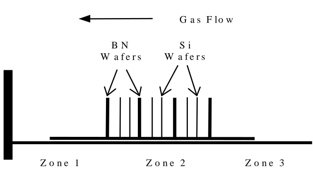
Boron Nitride Planar Diffusion Source System 2.1 Boron Nitride Solid Source Diffusion Process
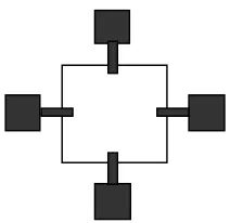
In a horizontal furnace, boron nitride planar diffusion source wafers and silicon
wafers are loaded perpendicular to the furnace tube axis onto a silica boat as shown
in the diagram below. Silicon wafers are placed adjacent to source wafers so that
only the front surface (device side) of the wafer is doped. During diffusion, a gas
flow, usually consisting of an inert gas such as nitrogen, is used to prevent the
entering of air contaminants into the tube. The flow of gas also creates a boundary
layer around the wafers, allowing the dopant vapor to be transported from the source
wafer to the silicon wafer by concentration gradient diffusion. Although nitrogen is
typically used for this purpose, gaseous mixtures of nitrogen, oxygen, and hydrogen
have also been used.
G a s F lo w
B N W a f e r s
S i W a f e r s
Z o n e 1 Z o n e 2 Z o n e 3
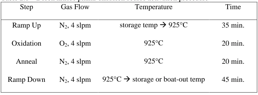
Table 2.1 – Boron nitride planar diffusion source activation procedure
Step Gas Flow Temperature Time
Ramp Up N2, 4 slpm storage temp
925 C 35 min.
Oxidation O2, 4 slpm 925 C 20 min.
Anneal N2, 4 slpm 925 C 20 min.
Ramp Down N2, 4 slpm 925 C
storage or boat-out temp 45 min.
The boron nitride source wafers used for this experiment were of a BN-975
grade designed by the Carborundum Corporation for use at temperatures between
800 and 1000 C. The source wafers are composed of boron nitride platelets held
together by a B2O3 binder. New boron nitride wafers undergo an activation
procedure as described in Table 2.1. The oxidation step forms a thin layer of B2O3
glass on the surface of the source wafer by the chemical reaction below:
4BN + 3O2
2B2O3 + 2N2 Eq. 2.1
The purpose for the anneal step is to stop the oxidation reaction above and stabilize
the rate of dopant volatilization. When not in use, the boron nitride source wafers
are stored in the furnace at 400 C with a N2 flow rate of 1500 sccm.
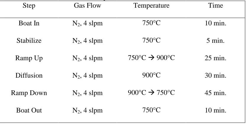
The general steps followed for a boron diffusion run are outlined in Table 2.2.
Note that the diffusion ambient gases, temperatures, and times are varied in the
experimental work for this thesis. The information given for these variables in the
table is the standard used at the Microelectronics Laboratory. During the diffusion
Table 2.2 – General boron diffusion procedure
Step Gas Flow Temperature Time
Boat In N2, 4 slpm 750 C 10 min.
Stabilize N2, 4 slpm 750 C 5 min.
Ramp Up N2, 4 slpm 750 C 900 C 25 min.
Diffusion N2, 4 slpm 900 C 30 min.
Ramp Down N2, 4 slpm 900 C 750 C 45 min.
Boat Out N2, 4 slpm 750 C 10 min.
and is transferred to the adjacent silicon wafer. A layer of B2O3 then forms on the Si
wafer surface and acts as the boron dopant source during diffusion. The following
interface reaction occurs:
2B2O3 + 3Si 4B + 3SiO2 Eq. 2.2 Depending on diffusion conditions, the following reactions may also occur:
Si + B Si-B phase Eq. 2.3
Si-B phase + O2 B-Si-O glass Eq. 2.4
Si + O2 SiO2 Eq. 2.5
Figure 2.2 is a schematic of the structure that is expected to form during
diffusion. The Si-B phase may or may not be present depending on diffusion
S i-B phase B -S i-O m ixture
S i su bstrate
Figure 2.2 – Schematic of structure formed on Si wafer during boron diffusion
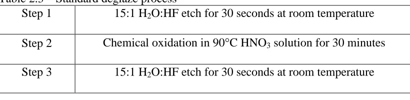
2.2 Deglaze Process
The deglaze is the process followed for the removal of diffusion byproducts.
The standard deglaze process used at the Microelectronics Laboratory is shown in
Table 2.3. Steps 1 and 3 involve the immersion of processed wafers in a
hydrofluoric acid solution for the etching of BSG. For the wafers processed in this
thesis study, a 15:1 H2O:HF solution was used for this purpose. Solutions of varying
HF concentrations, and even buffered oxide etch (BOE) solutions, have been used in
the past for deglaze. At Carborundum, a 10:1 HF solution is used for the BSG etch
step. A more dilute solution was used in this experiment to obtain a slower etch rate
and prevent the etching of field and gate oxides on device wafers.
Table 2.3 – Standard deglaze process
Step 1 15:1 H2O:HF etch for 30 seconds at room temperature
Step 2 of the deglaze process involves the immersion of wafers in a hot nitric
acid solution. Nitric acid, a very strong oxidizing agent, is brought to a temperature
of 90 C (slightly above its boiling point) using a hot plate. This nitric acid step acts as a form of oxidation and is needed to oxidize the Si-B layer that may have formed
during diffusion. The Si-B layer reacts with oxygen, producing a boron silicon glass
mixture (BSG), which can then be etched away by the HF solution used in step 3 of
the deglaze.
The use of nitric acid for the oxidation of the Si-B layer has been used
effectively in the past. However, a low-temperature thermal oxidation is the
preferred method of oxidizing this layer and is used at Carborundum. The
disadvantages to a thermal oxidation process include a further drive-in of the
junction and a possible depletion of boron dopants at the silicon surface. This boron
depletion can occur because boron has an affinity to oxide, which results in an
accumulation of boron in the oxide and therefore a depletion of boron in the silicon
substrate at the Si-SiO2 interface. However, this boron depletion effect may not be
significant at low temperatures. The results of the experimental work for this thesis
will help evaluate the effectiveness of the Microelectronics Laboratory standard
CHAPTER III
Experimental Approach 3.1 Experimental Design
The main approach used to achieve the experimental objectives in this thesis
was to examine the effects of the diffusion conditions explored in this experiment on
the formation of the silicon-boron phase and on device characteristics. The results of
this study will allow the determination of an optimum process for the doping of poly
gates and implants. The variables in the experiment include diffusion ambient,
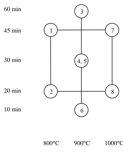
temperature, and time. Points were chosen in a modified central composite design as
shown below to achieve the experimental goals with the least number of wafers.
3
7 1
4, 5
8 2
6
800 C 900 C 1000 C 45 min
20 min 30 min 60 min
10 min
The experimental design shown in Figure 2.1 determined the diffusion
temperatures and times that would be carried out in the experiment. The temperature
range explored was 800 C to 1000 C, since the BN-975 grade planar diffusion sources used in the experiment were designed for use in this range. Times of
diffusion up to 60 minutes were used, since a diffusion time of greater than one hour
would require too high of a thermal budget for practical use. This design for
temperature and time was carried out for two different diffusion ambients: 1) a pure
nitrogen atmosphere and 2) a nitrogen-oxygen gaseous mixture. Note that although
only 7 points were explored in each ambient, the center point of the design was
repeated to address the issue of repeatability, resulting in 8 different diffusion
temperatures and times per ambient. The complete experimental design resulted in a
total of 16 diffusion runs.
In order to prevent the over-oxidation of the boron nitride solid source wafers,
the diffusion runs carried out in a nitrogen-oxygen gas ambient were broken down
into two steps. For the first half of the diffusion time, the doping process was
performed in a N2O2 environment. The second half of the diffusion time was carried
out in a pure nitrogen ambient. During diffusion processes, a presence of oxygen in
the atmosphere will oxidize the BN wafers as discussed in Chapter II. As in the
activation procedure followed for new BN wafers, an anneal in nitrogen is needed to
stop the oxidation process and stabilize the rate of dopant volatilization. For this
reason, a diffusion run in an oxidizing atmosphere should be followed by an anneal
in nitrogen at the diffusion run temperature. In order to preserve the structure for our
down into the two step N2O2/N2 process, within the diffusion time originally
designated.
For each of the 16 diffusion conditions in the experiment, one wafer would
undergo an entire device fabrication sequence. Devices would be fabricated on only
half of this wafer while the other half would be left blank for the purpose of
obtaining four-point probe measurements. The testing of capacitors and test
structures would allow the extraction of important electrical characteristics. An
additional blank wafer (monitor wafer) for each diffusion run would be processed
that would be used for materials characterization purposes such as transmission
electron microscopy (TEM) and spreading resistance analysis (SRA). Note that two
wafers were processed for each of the 16 diffusion runs – one monitor wafer and one
device wafer.
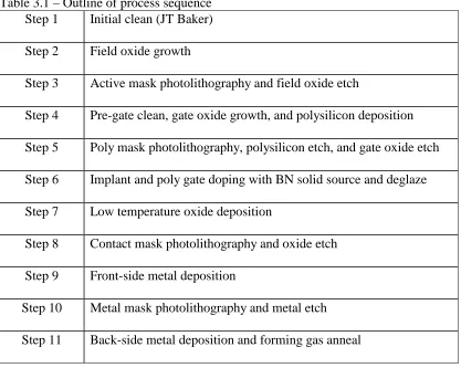
3.2 Wafer Processing
Devices were fabricated using the ECE 539 class mask set for the spring of
1998. The device fabrication process for this mask set is a four mask level process:
active, poly, contact, and metal. A detailed description of the process sequence is
given in Appendix A. Table 3.1 is a general outline of the major steps in the device
process flow. As explained in the previous section, devices were fabricated on only
half of the wafer so that four-point probe measurements could be obtained from the
Table 3.1 – Outline of process sequence Step 1 Initial clean (JT Baker)
Step 2 Field oxide growth
Step 3 Active mask photolithography and field oxide etch
Step 4 Pre-gate clean, gate oxide growth, and polysilicon deposition
Step 5 Poly mask photolithography, polysilicon etch, and gate oxide etch
Step 6 Implant and poly gate doping with BN solid source and deglaze
Step 7 Low temperature oxide deposition
Step 8 Contact mask photolithography and oxide etch
Step 9 Front-side metal deposition
Step 10 Metal mask photolithography and metal etch
Step 11 Back-side metal deposition and forming gas anneal
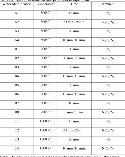
Blank wafers used for materials characterization techniques went through a BN
solid source diffusion run using the standard process explained in Chapter II. One
monitor wafer was used for each diffusion run. Table 3.2 is a list of all 16 diffusion
runs performed in this experiment. These blank wafers were cleaved in half, and a
modified deglaze etch was performed on one half of the wafer. This modified
deglaze simply included a 1 second dip in water followed by a 30 second etch in a
15:1 HF solution. This modified deglaze would be compared to the standard deglaze
by means of four-point probe and optical measurements as will be discussed in the
Table 3.2 – List of 16 diffusion runs performed in experiment
Wafer Identification Temperature Time Ambient
A1 800 C 45 min. N2
A2 800 C 20 min./25min. N2O2/N2
A3 800 C 20 min. N2
A4 800 C 10 min./10 min. N2O2/N2
B1 900 C 60 min. N2
B2 900 C 30 min./30 min. N2O2/N2
B3 900 C 30 min. N2
B4 900 C 15 min./15 min. N2O2/N2
B5 900 C 30 min. N2
B6 900 C 15 min./15 min. N2O2/N2
B7 900 C 10 min. N2
B8 900 C 5 min./5 min. N2O2/N2
C1 1000 C 45 min. N2
C2 1000 C 20 min./25min. N2O2/N2
C3 1000 C 20 min. N2
C4 1000 C 10 min./10 min. N2O2/N2
Note: The diffusion runs were not necessarily performed in this order. Runs were completed in a random fashion to reduce experimental biases. The Wafer
from the wafer surface before obtaining optical measurements of the BSG layer.
After diffusion, a hazy surface appeared on processed wafers which was caused by
the hydration of unreacted B2O3 on the Si wafer surface. The removal of this hazy
layer, which could be achieved by dipping the wafers in water, was needed to obtain
accurate optical measurements.
In the following sections, a brief description of the materials and electrical
characterization methods used in this experiment to obtain the desired data is given.
Testing procedures and conditions are given for each method.
3.3 Characterization Methods Used on Monitor Wafers
The blank wafers processed for each diffusion run were cleaved in half, as
previously explained. The half of the wafer that underwent the modified deglaze
process was used mainly for sheet resistance and BSG film thickness measurements.
The procedure and instruments used for these measurements will be described in
detail in the following appropriate sections. The half of the wafer that did not go
through a deglaze provided samples for transmission electron microscopy (TEM)
work, spreading resistance analysis (SRA), and x-ray diffraction (XRD) analysis.
3.3.1 Transmission Electron Microscopy
TEM was used in this experiment to obtain an image of the structure formed
on the silicon wafer by the BN solid source diffusion process. Low magnification
images provided by TEM would be able to verify the BSG/Si-B/Si sample
of an amorphous surface layer on the Si substrate would correspond to the BSG
layer. At high magnifications, the lattice structure of the single crystal Si substrate
could easily be imaged and any crystal defects at the Si surface caused by the
doping process could be detected. The presence of the Si-B phase would be
indicated by a crystalline layer sandwiched between the BSG film and the Si
substrate.
Although the presence of the Si-B phase can be verified by a hydrophilic Si
surface after the initial HF etch in the deglaze, methods of characterizing this layer
have not been well established. An exact index of refraction is not known for the
Si-B phase, and hence any optical methods used for measuring the thickness of this
layer will not give accurate results. Therefore, TEM was the chosen method to
extract Si-B layer thickness. In addition, because Carborundum has reported Si-B
layer thicknesses of 100 Å or less, the high resolution attainable by TEM methods
was essential in order to characterize the Si-B layer.
Since TEM is a very time consuming and expensive characterization
technique, images were not obtained from all samples. The wafers processed in a
N2 ambient were chosen to determine a general relationship between the Si-B layer
thickness and the diffusion temperature and time. From these wafers, the 3 that
were doped at 900ºC (not including the 30 min. replicate run) were imaged. These
3 points would allow the determination of a general model for the relationship
between Si-B phase formation and diffusion time. This model would enable the
A Si-B thickness for a wafer doped at 900ºC for 45 minutes could be extrapolated
from the diffusion time model, and this thickness could then plotted with the
thicknesses obtained from the two wafers doped for 45 minutes at 800ºC and
1000ºC. A general model of the effect of diffusion temperature on Si-B phase
formation could then be determined.
To verify that the temperature and time models extracted from the N2 data
were consistent in a mixed nitrogen-oxygen ambient, several wafers that were
processed in the N2O2 ambient were randomly chosen and imaged by TEM. The
samples imaged will be given in Chapter IV along with a discussion of the results
obtained from these images.
3.3.2 Optical Measurements
Optical measurements were performed on the half-wafer samples that
underwent the modified deglaze process as previously described in Section 3.2. A
Nanospec/AFT Nanometrics microscope was used for these measurements. This
instrument scans across an incident light wavelength from 480 to 790 nm, which is
reflected by the film, producing a pattern of interference fringes. The amplitude
and frequency of the sinusoidal pattern depends on the substrate and film thickness
being measured. A number of algorithms have been programmed for the
measurement of certain film thicknesses with the Nanometrics. The program used
to make all optical measurements on the half-wafer samples was an “oxide on Si”
Measurements were made before and after the samples underwent the
modified deglaze. It was assumed that the Nanometrics program used was
sufficient for the measuring of BSG thicknesses using an index of refraction of
1.46. The optical properties of BSG are very similar to that of SiO2 since this glass
is simply an amorphous silicon oxide with a high boron content. The presence of
boron will have a slight effect on the index of refraction of SiO2, but the use of this
algorithm for BSG thickness measurements will give reasonably good estimates.
The measurements obtained from these measurements are compared to extracted
BSG film thicknesses from TEM images in Chapter IV.
Optical measurements of each half-wafer sample were performed twice, once
after the water dip and once after the HF etch. This was done to determine the
effect of the initial HF dip on boron diffusion byproducts. A remaining film on the
Si wafer after this initial HF etch would indicate the presence of the Si-B phase.
3.3.3 Four-Point Probe Measurements
Sheet resistance measurements were also done for the half-wafer samples that
underwent the modified deglaze process using a four-point probe instrument. The
assumption was made that by using a half-blank wafer for sheet resistance
measurements with the four-point probe, correction factors for sample geometry
would not need to be taken into account.
The Si-B phase that may form during boron diffusion is known to be a
sample with a Si-B layer would be lower than that for an identically doped sample
without a Si-B surface layer. The four-point probe is measuring the lower
resistivity of the Si-B layer in parallel with the junction layer, thus resulting in an
overall lower resistivity. By comparing the sheet resistance of the half-wafer
samples that undergo the modified deglaze process to the sheet resistance of the
device wafers that undergo the standard deglaze, we are able to evaluate the
effectiveness of the nitric acid oxidation step in removing the Si-B phase.
3.3.4 X-Ray Diffraction
Small samples were cleaved from the half wafer that did not go through a
deglaze. An x-ray diffractometer with a CuK x-ray source was used to detect the presence of the Si-B phase. The samples were first dipped in concentrated HF to
remove BSG so that the signal intensity of the Si-B phase would not be
diminished. X-ray scans of diffraction angles (2 ) between 20 and 70 were first performed. However, because of Si-B layers of 100 Å or less were expected,
smaller scans between 30 and 35 were done at a slower scan rate to increase
signal intensity. The most intense peaks of the Si-B phases lay in this 2 range.
3.3.5 Spreading Resistance Analysis
Samples were sent to Solecon Laboratories, Inc., for spreading resistance
analysis for the purpose of obtaining resistivity and dopant profiles. Because this
technique is expensive, certain samples were selected for this analysis method. To
carrier concentration, the three samples doped at 900 C and the two doped at 800
and 1000 for 45 minutes for each diffusion ambient were selected for analysis. This was done for the same reasoning previously described in Section 3.3.1 when
choosing samples that would be imaged by TEM
.
3.4 Characterization Methods Used on Device Wafers
One half of each device wafer was left blank for four-point probe
measurements. Optical measurements were also performed on this blank half of the
wafer for reasons that will be given in the appropriate following sections. The
devices tested for electrical characteristics include metal-oxide-semiconductor
(MOS) capacitors and van der Pauw test structures.
3.4.1 Capacitance-Voltage Measurements
The MOS capacitors fabricated were tested for capacitance-voltage (CV)
characteristics. The definition of capacitance is
dV dQ
C Eq. 3.1
where dQ is the change in charge due to a change in voltage, dV. During CV
measurements, a small amplitude ac voltage superimposed on a dc bias is applied
to the gate metal contact. The ac voltage creates a change in charge and thus, a
capacitance is measured. The dc bias determines the region of device behavior,
e.g., accumulation, depletion, or inversion. Since the bias is applied to the gate, the
G G dV dQ C Eq. 3.2
where QG is the gate charge and VG is the gate voltage. In a MOS structure, charge
neutrality requires that the gate charge be compensated for by an equal and
opposite charge in the remaining areas of the structure (the oxide, the
semiconductor, and the oxide-semiconductor interface):
it ox s
G Q Q Q
Q
Eq. 3.3
where Qs is the charge in the semiconductor, Qox is the charge in the oxide, and Qit
represents interface trapped charges that are present at the Si-SiO2 interface due to
defects and impurities. In an ideal situation, there are no oxide charges present, and
therefore Qox = 0. Assuming this ideal case, the gate voltage becomes –(Qs + Qit).
By Kirkhoff’s law, the following relationship must apply:
s ox
G V V
V
Eq. 3.4
where Vox is the voltage drop across the oxide and Vs is the voltage drop across the
semiconductor. With the above expressions for QG and VG, the measured
capacitance for the CV measurements can be written as:
S OX it S dV dV dQ dQ C Eq. 3.5
which can also be written as
it s s it s ox dQ dQ dV dQ dQ dV C
1 Eq. 3.6
The charge in the semiconductor, in general, is due to hole charge QP, space-charge
region bulk charge QB, and electron charge QN. Therefore, the capacitance can be
it B N P S it S OX dQ dQ dQ dQ dV dQ dQ dV C
1 Eq. 3.7
Using the general definition for capacitance, the above equation becomes
it N B P
ox C C C C
C
C ! ! !
!
"
1 1
1 Eq. 3.8
Our MOS devices were fabricated on a n-type substrate. Therefore, for
positive gate voltages, the semiconductor surface is heavily accumulated with
electrons and QN dominates, resulting in a very large value for CN. The total
capacitance measured is then approximately equal to Cox. For small negative gate
voltages, the surface is depleted and the charge due to the space-charge region
charge, QB, dominates. The trapped interface charge capacitance also contributes
to the measured capacitance. The total capacitance is the combination of Cox in
series with CB in parallel with Cit. When CP begins to appear in weak inversion,
the total capacitance becomes:
it N B
ox C C C
C
C ! !
!
"
1 1
1 Eq. 3.9
In strong inversion, which occurs at negative gate voltages for n-type
substrates, QP dominates and CP becomes very large. The low-frequency (LF) CV
curve results if the inversion charge QP is able to follow the applied ac voltage. In
this case, the total capacitance once again becomes Cox as in the accumulation
region. When QP is unable to follow the high frequency of the applied ac voltage,
the high-frequency (HF) CV curve. If the voltage ramp rate is so high that no
inversion charge can form, a deep depletion CV curve is produced.
Using the Keithley CV tester, low frequency and high frequency CV curves
were obtained for the following MOS capacitors sizes: 100 # m x100 # m, 200 # m
x 200 # m, 300 # m x 300 # m, and 500 # m x 500 # m. Five capacitors for each size
were measured and an average CV curve was calculated. The average high
frequency CV curves for the 500 # m x 500 # m devices were later inputted into a computer program developed by Dr. John Hauser, a professor in the Electrical
Engineering Department at NCSU, that is able to extract flatband voltage from the
inputted data and calculate poly depletion effects. For the capacitance
measurements, the bias was ramped from +3 V to –3 V (from accumulation to
inversion) with a 20 mV voltage step and a time delay of 0.07 seconds, resulting in
an approximate ramp rate of 0.286 V/sec.
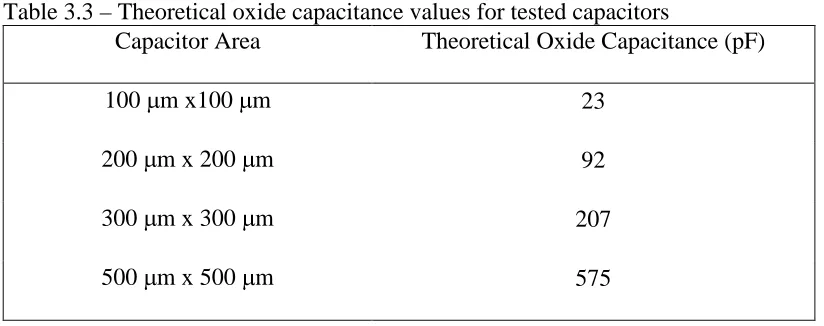
The capacitance of a material is
d A C $ % Eq. 3.10 where $
is the permittivity of the material, A is the cross-sectional area, and d is the
material layer thickness. The theoretical value for the oxide capacitance for the
device wafers used in this experiment can therefore be calculated, assuming an
oxide permittivity of
$
ox = 3.9 x
$
o, where
$
o is the permittivityof vacuum (8.85 x
10-14 F/cm). Solving for the oxide capacitance using the average oxide thickness
measured on the gate monitor wafer (150 Å), we obtain the values listed in Table
linear and have a slope approximately equal to & ox/tox, where tox is the gate oxide thickness. These plots were constructed for each device wafer to characterize the
quality of each doping process.
The theoretical flatband voltage for our MOS devices is simply equal to the
metal-semiconductor work function, assuming no oxide charges. To calculate the
metal-semiconductor work function, a further assumption that the polysilicon is
degenerately doped (' p=0.56V) is assumed. According to the wafer manufacturer of the silicon wafers used to fabricate the device wafers, the doping level of the
substrate is approximately 1 x 1016 cm-3. Therefore using the equation
D i s
N n q kT
ln
(
' Eq. 3.11
a value of -0.348 V for the substrate potential, ' s, is calculated, where ND is the
substrate doping level, ni is the intrinsic carrier concentration (1.45 x 1010 cm-3),
Table 3.3 – Theoretical oxide capacitance values for tested capacitors
Capacitor Area Theoretical Oxide Capacitance (pF)
100 ) m x100 ) m 23
200 ) m x 200 ) m 92
300 ) m x 300 ) m 207
Figure 3.2 – Schematic of the van der Pauw structure tested for sheet resistance data
and kT/q is 0.0259 V. This gives a metal-semiconductor work function * ms of:
V ms 0.56 ( 0.348)+ 0.908
,
,
+
* Eq. 3.12
Any deviations of experimentally extracted flatband voltages from this theoretical
value may be attributed to gate oxide charges.
3.4.2 Van Der Pauw Measurements
A schematic of the van der Pauw structure tested on all wafers is shown in
Figure 3.2. The poly van der Pauw structures were tested, from which we obtained
sheet resistance, - s, for the doped poly. A current, I, was applied across two adjacent contacts and the voltage, V, was then measured across the two remaining
contacts. Since the structure is symmetrical, the sheet resistance can be calculated
from the following relationship:
By using the resistivity vs. doping concentration plot given in Semiconductor
Material and Device Characterization by D. K. Schroder, developed for
boron-doped Si, an estimation of poly doping can be obtained with the use of the van der
Pauw sheet resistance values.
3.4.3 Four-Point Probe Measurements
At the end of the device fabrication sequence, sheet resistance measurements
with the four-point probe were obtained on the blank half of the device wafers. In
Chapter IV, these measurements are compared to sheet resistance measurements
from etched half-wafer samples using the modified deglaze process.
3.4.4 Optical Measurements
Optical measurements of the blank side of the device wafer were acquired
using the “oxide on Si” program at the end of the device fabrication sequence.
This was done to verify the absence of all diffusion byproducts from the wafer
surface. As will be discussed in Chapter IV, some wafers did not dewet after the
deglaze. This hydrophilic surface was assumed to indicate the presence of the Si-B
CHAPTER IV
Experimental Results and Discussion
4.1 Transmission Electron Microscopy Results
The TEM work completed as was described in Chapter III showed the presence
of a thick amorphous layer (BSG) on the Si substrate for all samples. Not all
samples imaged, however, showed the presence of a Si-B crystalline layer
sandwiched between the BSG and Si substrate. The only sample showing this layer
(of the nitrogen ambient processed samples imaged) was the sample doped at
1000> C for 45 minutes. This result confirms that the hydrophilic surface of this wafer after the deglaze was due to the presence of Si-B. Images show that this layer
was very non-uniform and caused a rough surface on the Si. Because of this severe
non-uniformity, an exact thickness could not be extracted for the Si-B layer. An
image of a sample doped in the nitrogen-oxygen ambient at 1000> C for 45 minutes
showed a similar structure to the 1000> C/45 min./N2 sample and is shown in Figure 4.1. From these two images, the Si-B layer thickness seemed to be on the order of 50
Å.
Images for two additional samples doped in the nitrogen-oxygen ambient were
obtained (800> C/45 min. and 900> C/30 min.) These images confirmed the
non-presence of a Si-B layer for samples doped under 1000> C. An additional observation
for the 900> C/60 min./N2 and 900> C/30 min./N2O2 samples is significant distortion
at the Si-SiO2 interface, which may allow for the formation of defect levels in
BSG layer thicknesses were extracted from TEM images. Although the
method of extraction was very susceptible to errors, the measurements were expected
to give reasonable estimations of the actual BSG layer thickness. In the following
section, these measurements will be compared to the optical measurements of the
BSG layer.
4.2 Optical Measurements
The BSG thickness measured for each sample is given in Table 4.1. For
samples C1 and C3, a measurement could not be obtained with the “oxide on Si”
program. The presence of Si-B is partly the reason for this result. An additional
reason may be the rough Si surface due to the non-uniformity of the Si-B phase. A
possible reason as to why this same effect was not encountered for the C2 and C4
samples is that the oxygen content in the atmosphere had some kind of effect on the
uniformity of the Si-B layer. Thus, the Si wafer surface did not have the amount of
roughness encountered in the wafers doped in nitrogen only. A qualitative
comparison of the TEM images for C1 and C2 seem to support this idea (see
Appendix B for TEM images).
As is expected, Table 4.1 shows that, in general, BSG thickness increases with
temperature and time. At the higher diffusion temperatures, the presence of oxygen
in the atmosphere resulted in a thicker BSG layer because of the additional oxide
formed from the reaction between oxygen and the Si substrate. This effect was not
Table 4.1 – BSG thickness measurements
Sample Optical TEM
A1 (800A C/45 min./N2) 536 521
A2 (800A C/45 min./N2O2) 452
--A3 (800A C/20 min./N2) 482
--A4 (800A C/20 min./N2O2) 473 417
B1 (900A C/60 min./N2) 1166 885
B2 (900A C/60 min./N2O2) 1391
--B3 (900A C/30 min./N2) 1284
--B4 (900A C/30 min./N2O2) 1357 1133
B5 (900A C/30 min./N2) 1329 1029
B6 (900A C/30 min./N2O2) 1104
--B7 (900A C/10 min./N2) 942 841
B8 (900A C/10 min./N2O2) 1065
--C1 (1000A C/45 min./N2) -- 2537
C2 (1000A C/45 min./N2O2) 3773
--C3 (1000A C/20 min./N2) --
--oxidation of the Si substrate may increase the BSG thickness at first, but as time of
diffusion increases, the slow diffusion of boron through the oxide layer greatly
reduces the amount of boron reaching the Si surface, and therefore results in less
formation of BSG.
Optical measurements made on the blank side of device wafers verified the
removal of diffusion byproducts for all wafers except the 1000B C/45 min./N2 doped wafer. A thickness was returned when using the “SiO2 on Si” program. Although
the actual value of this returned thickness is not any kind of accurate measurement of
the layers present on the Si surface, they reveal the presence of the Si-B phase on the
surface that should have been removed by the deglaze. This was also the only wafer
that remained a brownish yellow color after the deglaze. Therefore, we can conclude
that at this diffusion condition, the standard deglaze process is not effective. Table
4.2 is a comparison of the optical measurements obtained from the device wafers and
from the half-wafer samples that underwent the modified deglaze etch. Only the
samples for which a thickness value was returned after the deglaze etch are reported.
Table 4.2 – Optical measurements on deglaze etched samples
Diffusion Condition Device Wafer Half-Wafer Blank
1000B C/45 min./N2 551 Å 610 Å
1000B C/45 min./N2O2 <100 Å 282 Å
1000B C/20 min./N2 <100 Å 384 Å
For all other samples, a “less than 100 Å” measurement was returned since this is the
resolution limitation for the “Si on SiO2” program. From this data, we can conclude
that all wafers doped at 1000C C were the only wafers that formed the Si-B phase during diffusion. However, even though no film thickness was returned for the last 3
device wafers listed in Table 4.2, a hydrophilic surface indicates that the Si-B phase
is still present on these wafers after the deglaze. Therefore we can conclude that the
nitric acid oxidation is not effective in removing this layer.
4.3 Four-Point Probe Measurements
Sheet resistance values obtained from the four-point probe for both the device
wafers and the half-wafer samples are compared in Figure 4.3. No significant
difference between the wafers that underwent the standard deglaze and those that
underwent the modified deglaze etch is seen. For those wafers doped at 1000C C, a successful removal of the Si-B phase would be indicated by a higher sheet resistance
than that obtained from the samples simply etched in HF. This is not the case, and
thus further proves that the nitric acid step in the deglaze process may not be
effective in removing the Si-B layer from the Si wafer surface. For all samples, no
significant difference is seen between sheet resistance of monitor wafers and that of
device wafers.
Plots of log sheet resistance vs. log diffusion time for samples doped at 900C C
were constructed to establish a sheet resistance and time relationship. A linear fit to
1 10 100 1000
0 10 20 30 40 50 60 70
Diffusion Time (min.)
Sheet Resistance (ohms/sq.) Device, N2
Monitor, N2 Device, N2O2 Monitor, N2O2 800 C
900 C
1000 C
where n is a constant and t is the diffusion time in minutes. A high R2 value for this
linear fit would indicate a good model for the sheet resistance and diffusion time
relationship. Only those samples doped in a nitrogen atmosphere reported a high R2
value of 0.96 as shown in Figure 4.4. Therefore only for these samples could we
establish a relationship between sheet resistance and diffusion time. The slope of the
fitted line reveals that H sI t
1/5
. According to the R2 value, this model accounts for
96% of the variability in the data. Using this model, a value for a doped sample at
900J C for 45 minutes was extrapolated and used to construct a plot of log sheet resistance vs. 1/kT for samples of a 45 minute diffusion time. This plot shown in
Figure 4.5 also reveals a good linear fit, meaning that sheet resistance is proportional
to e1/kT.
Reasons for not being able to establish a temperature and time relationship for
samples doped in a nitrogen-oxygen ambient may include boron depletion from the
Si surface, thus affecting sheet resistance. Spreading resistance analysis results will
confirm this effect.
4.4 X-Ray Diffraction Results
For the x-ray diffraction scans performed on all samples, no Si-B diffraction
peaks were detected. We cannot conclude, however, that the reason for this result is
that there was no Si-B phase formed. Because all samples doped at 1000J C did not dewet after a long HF etch, it was expected that these samples would definitely show
y = -0.1905x + 2.2995 R2 = 0.9617
1.94 1.96 1.98 2 2.02 2.04 2.06 2.08 2.1 2.12
0 0.2 0.4 0.6 0.8 1 1.2 1.4 1.6 1.8 2
LOG Diffusion Time
LOG Sheet Resistance
y = 1E-19x - 5.2429 R2 = 0.9911
0 0.5 1 1.5 2 2.5 3
5.6E+19 5.8E+19 6E+19 6.2E+19 6.4E+19 6.6E+19 6.8E+19 7E+19 1/kT (1/J)
LOG Sheet Resistance
diffraction measurements is that the layer was too thin to produce x-ray signals of a
large enough intensity. This problem may be solved by using larger diffraction
and/or scattering slits. These slits control the size of the irradiated area and thus the
signal intensity. An additional solution would be to do scans at a slower rate than
used in this experiment.
4.5 Spreading Resistance Analysis Results
A total of ten samples were analyzed using SRA as described in Chapter III.
Relationships between the dose and diffusion time could not be established because
of the low R2 value returned for the plot of log dose versus log diffusion time. A log
junction depth vs. log diffusion time plot, however, did show a significant
relationship and is shown in Figure 4.6. Slopes of approximately 0.2 indicate that xj
is proportional to t1/5. A subsequent plot of log junction depth vs. 1/kT also revealed
a significant R2 value and is therefore a good model (Figure 4.7).
Dopant profiles obtained from the samples, shown in Appendix C, show an
increase in boron depletion at the Si wafer surface with diffusion time. In general,
the nitrogen-oxygen atmosphere seemed to enhance this depletion. This is most
likely due to the larger BSG thicknesses formed in an oxidizing atmosphere. In
addition, the diffusion of boron in silicon is enhanced in an oxidizing atmosphere,
and therefore accounts for the larger junction depths achieved for samples doped in
y = 0.1985x - 0.8273 R2 = 0.9097
y = 0.2214x - 0.9863 R2 = 0.959
-0.9 -0.8 -0.7 -0.6 -0.5 -0.4 -0.3 -0.2 -0.1 0
1 1.1 1.2 1.3 1.4 1.5 1.6 1.7 1.8 1.9
LOG Diffusion Time
LOG Junction Depth
N2 N2O2
Linear (N2O2) Linear (N2)
y = -1E-19x + 5.8788 R2 = 0.999
y = -8E-20x + 4.6449 R2 = 0.9934
-1.2 -1 -0.8 -0.6 -0.4 -0.2 0
5.6E+19 5.8E+19 6E+19 6.2E+19 6.4E+19 6.6E+19 6.8E+19 7E+19
1/kT (1/J)
LOG Junction Depth
N2 N2O2 Linear (N2O2) Linear (N2)
4.6 Capacitance-Voltage Measurements
Average high frequency CV curves for the 500 M m x 500 M m capacitors were obtained as explained in Chapter III. Figure 4.8 shows a typical HF curve obtained
from most device wafers. The actual measured CV curve and the CV curve after
correcting for polysilicon depletion effects are not significantly different. The most
significant differences in these curves was observed for the 900N C/60 min. diffusion runs in both gaseous ambients. HF CV curves for all samples are located in
Appendix D. Note that no data was obtained for wafers doped at 1000N C because no coherent data could be obtained from these devices. The device degradation may be
attributed to the presence of the Si-B phase.
In order to evaluate each doping process qualitatively, plots of Cox versus the
capacitor area were plotted. Note that the Cox values plotted are averages from five
measurements per capacitor area. A linear fit to the plotted points shows very high
R2 values for all devices. In addition, similar slopes of this plot were achieved
ranging from 2.26 x 10⁻⁷ F/cm2 to 2.36 x 10⁻⁷ F/cm2, resulting in tox values between
146 Å and 153 Å. This is very close to the average gate oxide thickness measured on
the gate monitor during the process flow (150 Å). See Appendix E for a Cox vs. area
plot for each device wafer.
Flatband voltages extracted from the 500 M m x 500 M m capacitor CV data are plotted in Figure 4.9 versus thermal budget. Using our theoretical calculation of a
flatband voltage of 0.908 V as a basis for determining an optimum process, the wafer
0.00E+00 1.00E+02 2.00E+02 3.00E+02 4.00E+02 5.00E+02 6.00E+02 7.00E+02
-3.00E+00 -2.00E+00 -1.00E+00 0.00E+00 1.00E+00 2.00E+00 3.00E+00 4.00E+00
Gate Voltage (V)
Capacitance (pF)
C Cdep
0 0.1 0.2 0.3 0.4 0.5 0.6 0.7 0.8
0 10000 20000 30000 40000 50000 60000
Thermal Budget (C-min.)
Flatband Voltage (V)
N2 N2O2
800C, 20min. 800C, 45min.
900C, 10min. 900C, 30min.
900C, 60min.
diffusion runs in N2 at a close second. Generally, flatband voltage shifts are
attributed to charges in the oxide. Significant shifts in the flatband due to positive
oxide charges occurred with the devices fabricated at 900P C. We can assume that boron penetration in the gate oxide is the reason for this large shift in the flatband.
Boron penetration may be occurring at the optimum 800ºC diffusion conditions as
well, but the effects are less significant in this case.
Low frequency CV curves were also obtained for each device wafer, but were
not analyzed because of unexplained anomalies in the curves. In inversion, the
measured capacitance did not become the oxide capacitance as it should have. It is
possible that the voltage ramp rate used to test the capacitors was too fast and did not
allow enough time for the device to reach equilibrium. Therefore, further testing of
the capacitors at a slower ramp rate should be completed to obtain low frequency CV
curves.
4.7 Van Der Pauw Measurements
Sheet resistance values for polysilicon were extracted from van der Pauw
measurements. The average polysilicon thickness measured on the poly monitor was
1398 Å. This thickness was used to obtain polysilicon resistivity from the sheet
resistance measurements:
t s Q R S
S
Eq. 4.2
A reference plot of resistivity vs. doping concentration for boron doped silicon was
then used to obtain a poly doping level from the calculated resisitivity values.
3 x 1019cm-3). A graph of poly doping versus the thermal budget (diffusion
temperature x time) is shown in Figure 4.10. Note that wafers doped at 1000T C did not produce functioning devices, and therefore, poly doping level could not be
extracted for these wafers. In general, higher values of poly doping were obtained
with the nitrogen diffusion ambient for wafers with equivalent thermal budgets.
The highest doping level of poly was achieved with the 900T C/60 min./N2 diffusion condition, but at the cost of a high thermal budget. Almost equivalent
levels of poly doping can be achieved at the 900T C/30 min/N2 and 900T C/10 min/N2 conditions. Since the poly doping at these conditions is in the 9 x 1019 cm-3 to 1 x
1020 cm-3 range, these are the optimum processing conditions for the doping of poly.
The 800T C diffusion runs showed only slightly lower levels of poly doping, but were still degenerately doped, with the runs in the nitrogen ambient showing the highest
1.00E+19 1.00E+20 1.00E+21
0 10000 20000 30000 40000 50000 60000
Thermal Budget (C-min.)
Poly Doping (cm
-3 )
N2 N2O2
900C, 10min
900C, 30min
900C, 60min
800C, 45min 800C, 20min
CHAPTER V
Summary and Conclusions 5.1 Summary
The main objective of this thesis was to determine an optimum process for the
boron doping of p-type implants and polysilicon gates of MOS devices using boron
nitride solid source diffusion. To achieve this goal, a design of experiments was
constructed that studied a wide range of diffusion conditions in which temperature,
time, and diffusion ambient were varied. MOS devices were fabricated at the 14
different diffusion conditions determined by the experimental design. A replicate run
was done at the center points of the design to address process repeatability, for a total
of 16 different runs. Monitor wafers were also doped at these 16 conditions.
Polysilicon van der Pauw test structures and MOS capacitors were tested on
all device wafers for the extraction of poly doping and flatband voltage. Information
could not be extracted from devices processed at 1000U C because they showed severe
degradation, most likely due to the presence of the Si-B phase. Consistent linear
plots of Cox vs. capacitance area showed an overall good quality process for the
device wafers. Severe shifts in flatband voltage were found for wafers doped at
900U C. Because shifts in flatband are due to oxide charges, the shift may be partially due to boron penetration in the gate oxide. Van der Pauw measurements gave poly
doping levels in the 1019 cm-3 and 1020 cm-3 range.
analysis gave dopant profiles for certain processing conditions. From SRA, models
for the relationship between junction depth and diffusion time and temperature were
established. A relationship between sheet resistance and diffusion time and
temperature was only established for the nitrogen gas ambient process. Four-point
probe and optical measurements were used to determine the presence of the Si-B
phase and evaluate the nitric acid oxidation step in the standard deglaze process. An
attempt was made to use x-ray diffraction to detect the Si-B phase layer but was
unsuccessful.
5.2 Conclusions
The optimal conditions for the doping of poly according to calculations from
van der Pauw measurements, occurred at the 900V C/60 min./N2 diffusion run. However, all diffusion conditions resulted in degenerately doped poly. Close to
theoretical flatband voltages were obtained from the runs performed at 800V C in a N2
ambient and at 800V C/20 min./N2O2. Taking all of these results into account, any
diffusion process performed at 800V C in a nitrogen ambient can be expected to give
good overall device characteristics. The lowest thermal budget would be achieved
with the 800V C/20 min./N2 diffusion process. Furthermore, the standard deglaze process used for this experiment should be modified since the nitric acid step did not
5.2 Future Work
The use of a statistical package to determine temperature and time models for
sheet resistance and dose should be explored. Further testing should be done of
MOS capacitors in an effort to verify the poly doping levels calculated through van
der Pauw measurements. This can be accomplished by obtaining low frequency CV
curves using a higher ramp rate than the one used in this experiment to ensure device
equilibrium during the test.
Modification of the deglaze etch should be carried out. A thermal oxidation
can replace the nitric acid step for the removal of the Si-B phase. The question
should be addressed as to whether an oxidation step is needed at all if the Si-B phase
is not formed. This may easily be done by fabricating devices that undergo an
oxidation step in the deglaze and comparing device characteristics, such as flatband
LIST OF REFERENCES
W. G. Allen, “Effect of oxidation on orientation-dependent boron diffusion in silicon,”
Solid State Electronics, Vol. 16, p. 709, 1973.
E. Arai, H. Nakamura, and Y. Terunuma, “Interface reactions of B2O3-Si system and
boron diffusion into silicon,” Journal of the Electrochemical Society: Solid-State Science
and Technology, Vol. 120, No. 7, p. 980, July 1973.
D. M. Brown and P. R. Kennicott, “Glass source B diffusion in Si and SiO2,” Journal of the Electrochemical Society: Solid State Science, Vol. 118, No. 2, p. 293, February 1971.
K. M. Busen, W. A. FitzGibbons, and T. Kloffenstein, “Removal of a silicon-boron phase which forms during deposition,” Electrochemical Technology,” Vol. 6, No. 7-8, p. 256, July-August 1968.
K. M. Busen, W. A. FitzGibbons, and W. K. Tsang, “Ellipsometric investigations of boron-rich layers on silicon,” Journal of the Electrochemical Society: Solid State
Science, Vol. 115, No. 3, p. 291, March 1968.
Carborundum Corporation, Boron Nitride PDS Products Literature, Carborundum Corporation, Amherst, NY, 1985.
T. P. Chen, T. F. Lei, H. C. Lin, and C. Y. Chang, “Characteristics of boron diffusion in polysilicon/silicon systems with a thin Si-B layer as diffusion source,” Journal of the
Electrochemical Society, Vol. 142, No. 2, p. 532, February 1995.
M. Crooke and A. G. K. Lutsch, “An expression for sheet resistivity using boron nitride source,” Journal of the Electrochemical Society: Solid-State Science and Technology, Vol. 124, No. 3, p. 457, March 1977.
B. D. Cullity, Elements of X-Ray Diffraction, second edition, Addison-Wesley Publishing Company, Inc., Philippines, 1978.
R. B. Fair, “Boron diffusion in silicon-concentration and orientation dependence, background effects, and profile estimation,” Journal of the Electrochemical Society:
Solid-State Science and Technology, Vol. 122, No. 6, p. 800, June 1975.
W. A. FitzGibbons, T. Kloffenstein, and K. M. Busen, “The effect of a silicon-boron phase on thermally grown silicon oxide films,” Journal of the Electrochemical Society:
M. Ghezzo and D. M. Brown, “Diffusivity summary of B, Ga, P, As, and Sb in SiO2,” Journal of the Electrochemical Society: Solid-State Science and Technology, Vol. 120,
No. 1, p. 146, January 1973.
A. S. Grove, O. Leistiko, Jr., and C. T. Sah, “Redistribution of acceptor and donor impurities during thermal oxidation of silicon,” Journal of Applied Physics, Vol. 35, No. 9, p. 2695, September 1964.
S. Horiuchi and J. Yamaguchi, “Diffusion of boron in silicon through oxide layer,”
Japanese Journal of Applied Physics, Vol. 1, No. 6, p. 314, December 1962.
R. C. Jaeger, Introduction to Microelectronic Fabrication, Addison-Wesley Publishing Company, Inc., Reading, Massachusetts, 1988.
T. Kato and Y. Nishi, “Redistribution of diffused boron in silicon by thermal oxidation,”
Japanese Journal of Applied Physics, Vol. 3, No. 7, p. 377, July 1964.
S. Maekawa and T. Oshida, “Diffusion of boron into silicon,” Journal of the Physical
Society of Japan, Vol. 19, No. 3, p. 253, March 1964.
J. F. Marchiando, P. Roitman, and J. Albers, “Boron diffusion in silicon,” IEEE
Transactions on Electron Devices, Vol. ED-32, No. 11, p. 2322, November 1985.
G. Masetti, S. Solmi, and G. Soncini, “Anisotropic boron diffusion in silicon under oxidizing atmospheres,” Solid State Communications, Vol. 12, No. 12, p. 1299, 1973.
G. Masetti, S. Solmi, and G. Soncini, “On the boron diffusivity versus silicon oxidation rate,” Japanese Journal of Applied Physics, Vol. 15, No. 12, p. 2471, 1976.
D. C. Montgomery, Design and Analysis of Experiments, fourth edition, John Wiley & Sons, Inc., New York, 1997.
W. A. Orr Arienzo, R. Glang, R. F. Lever, and R. K. Lewis, “Boron diffusion in silicon at high concentrations,” Journal of Applied Physics, Vol. 63, No. 1, p. 116, January 1988.
W. A. Rausch, R. F. Lever, and R. H. Kasti, “Diffusion of boron in polycrystalline silicon from a single crystal source,” Journal of Applied Physics, Vol. 54, No. 8, p. 4405, August 1983.
L. Reimer, Transmission Electron Microscopy: Physics of Image Formation and
Microanalysis, third edition, Springer-Verlag Berlin Heidelberg, Germany, 1993.
D. K. Schroder, Semiconductor Material and Device Characterization, John Wiley & Sons, Inc., New York, 1990.
K. Shimakura, T. Suzuki, and Y. Yadoiwa, “Boron and phosphorus diffusion through an SiO2 layer from a doped polycrystalline Si source under various drive-in ambients,” Solid
State Electronics, Vol. 18, p. 991, 1975.
J. Stach and A. Turley, “Anomalous boron diffusion in silicon from planar boron nitride sources,” Journal of the Electrochemical Society: Solid-State Science and Technology, Vol. 121, No. 5, p. 722, May 1974.
K. Suzuki, H. Yamawaki, and Y. Tada, “Boron out diffusion from Si substrates in various ambients,” Solid State Electronics, Vol. 41, No. 8, p. 1095, 1997.
K. M. Whittle and G. L. Vick, “Control of boron diffusion from a pyrolitic borosilicate glass source,” Journal of the Electrochemical Society: Solid State Science, Vol. 116, No. 5, p. 645, May 1969.
David B. Williams and C. Barry Carter, Transmission Electron Microscopy: A Textbook