ABSTRACT
GONG, BO. Atomic Layer Deposition and Molecular Layer Deposition on Polymers. (Under the direction of Gregory N. Parsons).
Atomic layer deposition (ALD) is a vapor phase thin film deposition technique based
on sequential self limiting surface reactions. In a typical ALD process, two reactants are
introduced alternatively to a substrate, resulting in formation of a single atomic layer each
exposure cycle. Repeating the surface-limiting reaction cycle allows ultra-uniform nanoscale
films to be formed with precise thickness control over complex 3D surfaces. Similar self
limiting surface reactions have been used for the deposition of polymer or organic-inorganic
hybrid films. This extended ALD process is described as molecular layer deposition (MLD).
In our studies, we are exploring new chemistry and applications of ALD/MLD.
Arrays of ALD/MLD processes have been conducted on various polymer substrates. By
coating the substrates with different materials, we were able to give new functionalities to the
polymers. For example, hydrophilic, conductive, and photocatalytic coatings have been
deposited. Moreover, recent studies of ALD on polymers showed that metal organic
precursors often diffuse sub-surface into the polymer. This sub-surface diffusion and reaction
could result in the change of the chemical composition and the physical properties of the bulk
polymer.
Surface functionalization and chemistry modification of polymers by ALD/MLD
enabled a large number of new applications of polymers. In this work, several demonstration
applications will be presented, and the mechanism of the ALD/MLD process on polymers
© Copyright 2012 by Bo Gong
Atomic Layer Deposition and Molecular Layer Deposition on Polymers
by Bo Gong
A dissertation submitted to the Graduate Faculty of North Carolina State University
in partial fulfillment of the requirements for the degree of
Doctor of Philosophy
Chemical Engineering
Raleigh, North Carolina
2012
APPROVED BY:
_______________________________ ______________________________ Dr. Gregory N. Parsons Dr. Saad A. Khan
Committee Chair
DEDICATION
To my parents, Weizhen Gong and Quanzhen Shi,
BIOGRAPHY
Bo Gong was born in Jiuquan, Gansu province, China on Oct 22nd, 1984. He
graduated with a Bachelor of Science in Chemical Engineering from Tianjin University in
July 2007. Following graduation he joined the Chemical and Biomolecular Engineering
Department at North Carolina State University. He will work with Novellus Systems Inc.
ACKNOWLEDGMENTS
I would like first to express my sincere appreciation to my advisor, Dr. Gregory N.
Parsons, for the freedom and his endless support and guidance through my PhD research and
studies. I also want to thank my committees, Dr. Saad A. Khan, Dr. Orlin D. Velev and Dr.
Michael D. Dickey, for their inspiring discussion and comments.
I would like to thank past members of the Parsons research group, Dr. Qing Peng, Dr.
Jeong-seok Na, Dr. Giovanna Scarel, Dr. Kevin Hyde, Dr. Kim Roberts, Dr. Sang-jeong Oh,
Dr. Jesse S. Jur, and Dr. Joe C. Spagnola, for their mentoring and instruction. I want to give
special thanks to Dr. Qing Peng. He introduced me to the ALD and helped me to get familiar
with everything in the lab. I also want to thank current members of the group, Dr. Chris
Oldham, Dr. Mark Losego, Christina Devine, Dohan Kim, Kyoungmi Lee, Will Sweet, Berc
Kalanyan, Moataz Mousa, Sarah Atanasov, and Junjie Zhao, for their helpful discussion and
collaborations.
I also want to thank staff at AIF (NCSU) and SMIF (DUKE), Chuck Mooney,
Roberto Garcia, Fred Stevie, Michelle Gignac, and Mark D. Walters, for their help with some
materials characterization. I am grateful to Laura Beth Dong for helping me understand the
BET equipment and analysis.
Last but not the least, I must acknowledge my family. I could not finish my PhD
TABLE OF CONTENTS
LIST OF TABLES ... x
LIST OF FIGURES ... xi
CHAPTER 1. Introduction ... 1
1.1 Overview of Thin Film Deposition Techniques on Polymers ... 1
1.1.1 Sol-gel ... 2
1.1.2 Hydrothermal ... 3
1.1.3 Layer by Layer ... 4
1.1.4 Electroless Plating ... 5
1.1.5 Spraying ... 5
1.1.6 Dip Coating ... 5
1.1.7 Physical Vapor Deposition ... 6
1.1.8 Chemical Vapor Deposition ... 6
1.2 Atomic Layer Deposition and Molecular Layer Deposition ... 7
1.2.1 Atomic Layer Deposition ... 7
1.2.2 Molecular Layer Deposition ... 8
1.3 Atomic Layer Deposition on Polymers and Sequential Vapor Infiltration ... 9
1.3.1 ALD Growth on Polymer Substrates ... 9
1.3.2 Sequential Vapor Infiltration ... 10
1.4 Integration of Atomic Layer Deposition and Liquid Phase Deposition Techniques .... 13
1.4.1 ZnO ALD and Hydrothermal Growth of ZnO Nanorods ... 13
1.4.2 Al2O3 ALD and Layer by Layer Growth of Metal Organic Frameworks ... 14
1.5 Opportunities of Atomic Layer Deposition and Related Processes. ... 15
References ... 22
CHAPTER 2. Experimental Tools ... 34
2.1 Atomic Layer Deposition and Molecular Layer Deposition Systems ... 34
2.2 Spin-coating and Electro-spinning of Polymers ... 35
2.2.1 Spin-coating of Polymer Films ... 35
2.2.2 Electro-spinning of Polymer Fibers ... 36
2.3 Liquid Phase Deposition Techniques ... 36
2.3.2 Layer by Layer MOF Assembly ... 37
2.4 Materials Characterization ... 37
2.4.1 Ellipsometry ... 37
2.4.2 Quartz Crystal Microbalance ... 38
2.4.3 Vibration Spectroscopy (FTIR, UV-Vis) ... 38
2.4.4 Electron Microscopes (SEM, TEM) ... 41
2.4.5 Atomic Force Microscope ... 42
2.4.6 Nitrogen Adsorption/ Desorption Analysis (BET) ... 42
2.4.7 Water Contact Angle ... 43
2.4.8 X-ray Photoelectron Spectroscopy (XPS) ... 44
2.4.9 X-ray Diffraction (XRD) ... 44
2.4.10 Mechanical Tensile Test ... 44
2.4.11 Thermal Gravity Analysis (TGA) and Differential Scanning Calorimetry (DSC) ... 45
References ... 49
CHAPTER 3. Overview of Key Results of the Dissertation ... 51
3.1 Conformal Organic-Inorganic Hybrid Network Polymer Thin Films by Molecular Layer Deposition using Trimethylaluminum and Glycidol ... 51
3.2 A Two-Step Lewis Acid-Catalyzed ε-Caprolactone Ring-Opening Molecular Layer Deposition Process for Hybrid Organic-Aluminum Oxide Polymer Thin Films ... 52
3.3 Highly Active Photocatalytic ZnO Nanocrystalline Rods Supported on Polymer Fiber Mats: Synthesis Using ZnO Atomic Layer Deposition and Hydrothermal Crystal Growth ... 53
3.4 Layer by Layer Growth of HKUST-1 on Nonwoven Polypropylene Fiber Mat ... 54
3.5 Atomic Layer Deposition of Aluminum Oxide on Metal Organic Framework Cu3(BTC)2 ... 56
3.6 Quantitative Analysis of Reaction of Trimethyl-aluminum towards Polymer Substrates during Al2O3 Atomic Layer Deposition by In-situ FTIR ... 57
3.7 Sequential Vapor Infiltration of Metal Oxides into Sacrificial Polyester Fibers: Shape Replication and Controlled Porosity of Micro/Mesoporous Oxide Monoliths ... 59
3.8 Hydrophilic Mechanical Buffer Layers and Stable Hydrophilic Finishes on Polydimethylsiloxane using Combined Sequential Vapor Infiltration and Atomic/Molecular Layer Deposition ... 61
3.10 Core Sheath Nanocomposite Structures Enabled by Aluminum Oxide Atomic Layer
Deposition on Bicomponent Polymer Fibers ... 64
CHAPTER 4. Conformal Organic-Inorganic Hybrid Network Polymer Thin Films by Molecular Layer Deposition using Trimethylaluminum and Glycidol ... 82
Abstract ... 83
4.1. Introduction ... 84
4.2. Experimental Section ... 87
4.3. Results and Discussion ... 90
4.4. Summary and Conclusions ... 99
Acknowledgments... 99
References ... 114
CHAPTER 5. A Two-Step Lewis Acid-Catalyzed ε-Caprolactone Ring-Opening Molecular Layer Deposition Process for Hybrid Organic-Aluminum Oxide Polymer Thin Films ... 119
Abstract ... 120
5.1. Introduction ... 121
5.2. Experimental Details ... 123
5.3. Experimental Results ... 126
5.4. Conclusions ... 131
Acknowledgments... 132
References ... 144
CHAPTER 6. Highly Active Photocatalytic ZnO Nanocrystalline Rods Supported on Polymer Fiber Mats: Synthesis Using ZnO Atomic Layer Deposition and Hydrothermal Crystal Growth... 149
Abstract ... 150
6.1. Introduction ... 151
6.2. Experimental Procedures ... 153
6.3. Results and Discussion ... 156
6.4. Summary and Conclusions ... 161
Acknowledgements ... 161
References ... 168
CHAPTER 7. Layer by Layer Growth of HKUST-1 on Nonwoven Polypropylene Fiber Mat ... 173
7.1. Introduction ... 175
7.2. Experimental ... 176
7.3. Experimental Results ... 179
7.4. Conclusions ... 183
Acknowlegment ... 183
References ... 189
CHAPTER 8. Atomic Layer Deposition of Aluminum Oxide on Metal Organic Framework Cu3(BTC)2 ... 195
Abstract ... 196
8.1. Introduction ... 197
8.2. Experimental ... 198
8.3. Results and Discussion ... 201
8.4. Conclusion ... 204
References ... 212
CHAPTER 9. Quantitative Analysis of Reaction of Trimethyl-aluminum towards Polymer Substrates during Al2O3 Atomic Layer Deposition by In-situ FTIR ... 216
Abstract ... 217
9.1. Introduction ... 218
9.2. Experimental Section ... 220
9.3. Experimental Results ... 224
9.4. Discussion ... 234
9.5. Summary ... 239
Acknowledgements ... 240
References ... 259
CHAPTER 10. Sequential Vapor Infiltration of Metal Oxides into Sacrificial Polyester Fibers: Shape Replication and Controlled Porosity of Micro/Mesoporous Oxide Monoliths ... 265
Abstract ... 266
10.1. Introduction ... 267
10.2. Experimental Procedures ... 269
10.3. Results and Discussion ... 274
References ... 295
CHAPTER 11. Hydrophilic Mechanical Buffer Layers and Stable Hydrophilic Finishes on Polydimethylsiloxane using Combined Sequential Vapor Infiltration and Atomic/Molecular Layer Deposition ... 301
Abstract ... 302
11.1. Introduction ... 303
11.2. Experimental Methods ... 305
11.3. Results and Discussion ... 307
11.4. Summary and Conclusions ... 312
Acknowledgements ... 313
References ... 319
CHAPTER 12. Directed Mesoporous Metal Oxides by Vapor Phase Atomic Layer Deposition and Infiltration of Ordered Surfactant Thin Films ... 322
Abstract ... 323
12.1. Introduction ... 324
12.2. Experimental Methods ... 326
12.3. Results and Discussion ... 329
12.4. Summary and Conclusions ... 334
References ... 344
CHAPTER 13. Core Sheath Nanocomposite Structures Enabled by Aluminum Oxide Atomic Layer Deposition on Bicomponent Polymer Fibers ... 349
Abstract ... 350
13.1. Introduction ... 351
13.2. Experimental Section ... 352
13.3. Experimental Results and Discussion: ... 356
13.4. Conclusion ... 359
Acknowledgments... 359
LIST OF TABLES
LIST OF FIGURES
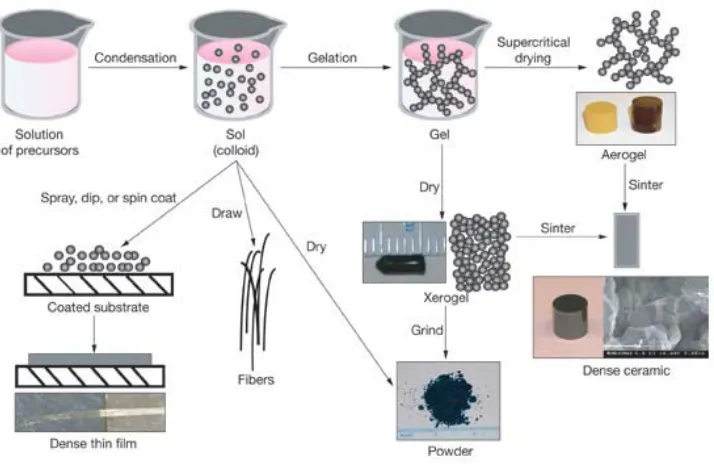
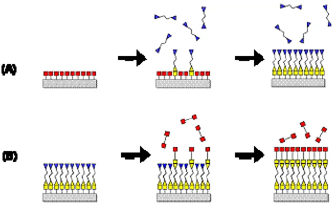
Figure 1.1. A overview of the sol gel process. In sol gel chemistry, molecular precursors are converted to nanoparticles to form a colloidal suspension, or sol. The gel network can be produced by further condensation. The gel can be processed by various drying methods to develop materials with distinct properties. (https://www.llnl.gov/str/May05/Satcher.html).. 18 Figure 1.2. The layer by layer (LBL) process and the structure of LBL films. 1) solution of positive polyelectrolyte, 2) pure deionized water, 3) solution of negative polyelectrolyte, 4) pure deionized water. ... 19 Figure 1.3. A schematic diagram of atomic layer deposition (ALD) of Al2O3. Trimethyl aluminum (TMA) and water are used as precursors to react with surface alternatively. ... 20 Figure 1.4. A schematic diagram for molecular layer deposition (MLD). (A) Organic
precursor A reacts with surface functional groups. (B) Organic precursor B reacts with precursor A saturated surface. ... 21 Figure 2.1. A schematic view of the viscous flow ALD/MLD reactor. The precursors are delivered into the reactor with Ar carrier gas. On the reactor exhaust line, computer
controlled gate values are used to direct the exhaust from the EG pulse into a liquid nitrogen trap before entering the pump. ... 46 Figure 2.2. Schematic diagram of In-situ FTIR ALD/MLD reactor. The precursors are delivered into the reactor with high purity Ar. In the middle part of the chamber, two CsI IR windows are attached, and two gate valves are installed between the IR window and reactor chamber to prevent the deposition of ALD/MLD film on the windows. During the
measurement, the IR beam is directed through the planar sample and focused into a MCT-A detector. Before each dose, a background spectrum was collected as reference, and
differential spectra were employed to show the surface chemistry change after each pulse. . 47 Figure 2.3. (a) An example nitrogen adsorption/ desorption isotherm collected by Autosorb-1C at 77K. (b) BET plot calculated from the adsorption isotherm.(0.05<P/P0<0.35) The BET surface area can be calculated from the intercept and the slope of the plot. ... 48 Figure 3.1. Schematic of the surface reactions during TMA/GLY MLD process consistent with the FTIR data in Figure 4.6(a). Exposing the –OH surface to TMA produced surface Al-CH3. The following glycidol exposure consumes Al-CH3 surface units, including reactions with both the OH and epoxy end of the molecule. The aluminum can help catalyze the ring opening. Available OH groups are then available to react with TMA during the next
exposure step. Not shown in this diagram is the expected sub-surface diffusion of TMA and reaction with available lone pair sites producing Lewis acid/base O: Al(CH3)3 adducts that can react during the next glycidol exposure step. ... 66 Figure 3.2. Direct comparison between in-situ QCM data collected during TMA/GLY, TMA/water/GLY and DEZ/GLY sequences following TMA/water (or DEZ/water) ALD. TMA (DEZ)/Ar/GLY/Ar = 1/40/2/40 s is used for TMA/GLY and DEZ/GLY, and
TMA/Ar/Water/Ar/GLY/Ar = 1/40/1/40/2/40 s is used for TMA/Water/GLY. The TMA/GLY produced an induction period followed by a large mass uptake. The TMA/water/GLY
Negligible mass uptake is observed for the DEZ/GLY sequence, demonstrating the
importance of the Al-CH3 as a growth catalyst. ... 67 Figure 3.3. Film thickness for TMA/LAC MLD films on silicon wafers is plotted versus number of MLD cycles at various growth temperatures. Film thickness was determined using ellipsometry. For all the samples on Si wafer the deposition sequence was TMA/Ar/LAC/Ar = 1/40/2/40 seconds. The growth rate decreased from 0.75 Å /cycle to 0.08Å/cycle as the substrate temperature increased from 60 to 120°C. ... 68 Figure 3.4. Scanning electron micrographs obtained from: (a) and (b), untreated PBT fibers after hydrothermal ZnO nanorod crystal growth; (c) and (d), PBT fibers after 100 ALD cycles of ZnO (~20 nm thick), followed by hydrothermal ZnO nanorod growth. Nanorod crystals are visible primarily on the top-most fibers in the fiber mat. Panels (e) and (f) show PBT fibers after 200 cycles (~40 nm) of ALD ZnO, followed by ZnO nanorod growth. Nanorod growth is visible on all the fibers. In panel (b) a circle highlights a large crystal, similar in size to the one shown in Figure 2(b), formed on the untreated fiber. ... 69 Figure 3.5. Normalized absorbance of organic dye at 525 nm plotted versus UV radiation exposure time. PBT fiber substrates with various surface treatments were immersed in the aqueous solution containing the azo dye (acid red 40), and illuminated using a UV lamp. The fibers with ALD ZnO and ZnO nanorod crystals produced the most rapid photocatalytic dye degradation. The inset shows a photograph of the dye solutions in contact with the different substrates after 2 hr of illumination. The red dye is nearly completely removed from the solution in contact with the nanorod-coated fibers. ... 70 Figure 3.6. Optical images of HKUST-1 coated PP fiber mat. (a) The fiber mat on the left is the direct LBL growth of MOF on PP fiber mat. The mat on the right is the PP fiber mat pretreated with ALO, then coated with MOF by LBL technique. (b) MOF coated PP fiber mat before vacuum dry. (c) MOF coated PP fiber mat after vacuum dry. ... 71 Figure 3.7. The Fourier transform infrared (FTIR) spectra collected from the HKUST-1 films on Al2O3 coated Si wafers. Slow growth was detected for the first 2 deposition cycles. Then the linear increase of IR absorbance vs. LBL deposition cycles was observed. ... 72 Figure 3.8. In-situ QCM data collected from water/N2 process on bare QCM and Cu3(BTC)2 particle coated QCM. Bare QCM crystal showed negligible mass uptake during water exposures, while the Cu3(BTC)2 coated QCM crystal showed very large mass uptake and decreasing. The MOF with 5 cycles of TMA/water ALD process showed smaller mass uptake during water exposure, and this could be explained by the shrinking of pore volume and size after ALD. ... 73 Figure 3.9. The Al-CH3 deformation (~1200 cm-1) and CH3 asymmetric stretching (~2960 cm-1) absorbance increase after first TMA pulse on different polymer substrate. The
with transformation of the polymer to micron-sized alumina fibers. Panel (b) shows a scanning electron microscope image of the as-received PBT nonwoven. Panels (c) and (d) show a similar sample after 1 h TMA/water soaking and 12 h 450°C anneal. The images in (c) and (d) show that the soaking and annealing preserves the starting fiber morphology. Some connectivity between the fibers likely results from polymer flow during the soaking process. More connectivity was observed with higher process temperature and longer
precursor exposure. The cross-sectional view in panel (d) confirms that the fibers are uniform after calcination, indicating full penetration of the precursor throughout the 3 µm diameter starting fiber. ... 76 Figure 3.11. FTIR transmission spectra collected in situ from the a starting PBT film cast onto a silicon substrate (bottom trace) and after exposing the film to TMA (middle) and water (upper trace) at 80°C. The TMA exposure removes ester (1720 and 1270cm-1) and ether (1100 cm-1) bonding units indicating high reactivity between TMA and ester bonds in the PBT. The CH3 (2860 and 2930 cm-1) and Al-CH3 modes (1200 cm-1) increase upon TMA treatment, confirming Al-CH3 present in the soaked PBT film. After water dosing, the
decrease in CH3 and Al-CH3 absorbance and an increase in Al-O modes shows water reacting with the Al-CH3 groups to form Al-OH. ... 77 Figure 3.12. Stress strain curve of TMA/water and DEZ/water soaked PDMS and pristine PDMS. The slope of the stress strain curve is the measure of the Young’s modules, we can see after soak with metal organic precursor, the modules of PDMS is significant increased. This increase of young’s modulus will form a mechanical buffer layer between ALD coating and bulk PDMS, which will stabilize the ALD coating and keep the ALD layer intact. ... 78 Figure 3.13. Schematic diagram of surface treatment of PDMS with ALD only or sequential vapor infiltration followed by ALD. The top scenario shows direct aluminum oxide ALD on PDMS resulting in cracked aluminum oxide coating. The bottom scenario shows ALD after sequential vapor infiltration, producing a smooth and uniform coating on the PDMS. The sequential vapor infiltration before the ALD helps maintain the surface in a hydrophilic state. ... 79 Figure 3.14. Schematic diagram for the preparation of mesoporous metal oxide materials from vapor phase infiltration method. ... 80 Figure 3.15. Schematic diagram of the “short” and “long” TMA/water ALD cycles on
PLA/PP core/sheath bi-component fibers. When the core/sheath fiber was exposed to “short” TMA/water exposures, precursor vapors were not given enough time to diffuse into the PP layer. Minimal subsurface diffusion and reaction occurred, and thin Al2O3 ALD layer was deposited on PP surface. However, when the “long” precursor exposures were used, TMA and water vapors could diffuse through the PP, and react with PLA core. ... 81 Figure 4.1. Schematic diagram of the in-situ FTIR ALD/MLD reactor. The precursors are delivered into the reactor with high purity Ar. In the middle part of the chamber, two CsI IR windows are attached, and two gate valves are installed between the IR window and reactor chamber to prevent the deposition of ALD/MLD film on the windows. During the
measurement, the IR beam is directed through the planar sample and focused into a MCT-A detector. Before each dose, a background spectrum was collected as reference, and
Figure 4.2. (a) Film thickness for TMA/GLY MLD films on silicon wafers is plotted versus number of MLD cycles at various growth temperatures. Film thickness was determined using ellipsometry. For all the samples on Si wafer the deposition sequence was TMA/Ar/GLY/Ar = 1/40/2/40 seconds. The growth rate decreased from 2.4 nm/cycle to 0.6 nm/cycle as the substrate temperature increased from 90 to 150 °C. (b) More careful examination shows the growth rate of the MLD film on silicon starts off slowly and increases over the first 100 cycles at 120 °C, before reaching steady state. The reflective index decreased with growth time, consistent with a less dense film structure and overall change in the growth reaction mechanism as deposition proceeds. ... 102 Figure 4.3. In-situ QCM mass uptake results for TMA/water ALD and TMA/GLY MLD sequences. Gas pulse and purge times were 1/40/2/40 seconds. (a) TMA/water ALD at 120 °C under steady-state growth, shows an average mass uptake during the TMA and water pulses of ~80 ng/cm2 and ~12 ng/cm2 respectively; (b) TMA/GLY MLD at 120 °C under steady-state growth shows a larger average mass uptake of ~210 ng/cm2 and ~118 ng/cm2 during the TMA and GLY pulses, respectively; (c) 100 cycles of TMA/GLY MLD at 90 to 150 °C on an Al-OH surface (formed using TMA/water ALD) shows an increase in
deposition rate at lower temperatures, and a growth incubation time. (d) Mass uptake per step for 100 cycles of TMA/GLY MLD at 120 °C on Al-OH surface. Approximately 60 cycles was needed for the TMA/GLY MLD process to reach steady growth, which is consistent with growth rate data collected from film on Si wafers. The small mass uptake of TMA and GLY at the very beginning implied the “double” reaction is happening on the surface. ... 103 Figure 4.4. In-situ QCM data for TMA and glycidol dose saturation during the TMA/GLY MLD process at 120 °C. (a) After multiple repeated cycles of TMA/GLY, the surface was repeatedly exposed to TMA/Ar pulses (TMA/Ar = 1/82 s). More than 16 pulses were needed to saturate the surface. (b) Similar experiments for glycidol dose saturation on TMA
saturated surface (GLY/Ar = 2/81 s). Both reagents showed high mass uptake for the first pulse. The data shows that after many growth cycles, both the TMA and GLY reagents diffuse subsurface and react during film growth. The subsurface diffusion is more prevalent in thicker films than in thinner films, but it becomes kinetically limited as film thickness increases. ... 104 Figure 4.5. Direct comparison between in-situ QCM data collected during TMA/GLY, TMA/water/GLY and DEZ/GLY sequences following TMA/water (or DEZ/water) ALD. TMA (DEZ)/Ar/GLY/Ar = 1/40/2/40 s is used for TMA/GLY and DEZ/GLY, and
TMA/Ar/Water/Ar/GLY/Ar = 1/40/1/40/2/40 s is used for TMA/Water/GLY. The TMA/GLY produced an induction period followed by a large mass uptake. The TMA/water/GLY
sequence showed a much lower mass uptake per cycle, without an induction period. Negligible mass uptake is observed for the DEZ/GLY sequence, demonstrating the
importance of the Al-CH3 as a growth catalyst. ... 105 Figure 4.6. In-situ differential FTIR spectra collected during (a) the first TMA/GLY
or epoxy groups on GLY. The increase of CH2 modes at 2865 and 2928 cm-1 confirms the attachment of GLY on the surface. In panel (b) the GLY dose after the water exposure produced an obvious decrease of surface -OH peak at 3700 cm-1 and increase of CH2 modes at 2865 and 2928 cm-1. The decrease of –OH indicates a reaction between the -OH on GLY and the Al-OH surface. (Fringes on the spectra is due to the interference from the AAO membrane). ... 106 Figure 4.7. Schematic of the surface reactions during TMA/GLY MLD process consistent with the FTIR data in Figure 4.6(a). Exposing the –OH surface to TMA produced surface Al-CH3. The following glycidol exposure consumes Al-CH3 surface units, including reactions with both the OH and epoxy end of the molecule. The aluminum can help catalyze the ring opening. Available OH groups are then available to react with TMA during the next
exposure step. Not shown in this diagram is the expected sub-surface diffusion of TMA and reaction with available lone pair sites producing Lewis acid/base O: Al(CH3)3 adducts that can react during the next glycidol exposure step. By placing a water exposure step after the TMA exposure, the subsurface Al-CH3 groups become “quenched” and result in more steady growth at a reduced growth rate, as shown in the QCM data in Figure 4.5. ... 107 Figure 4.8. (a) Ex-situ FTIR spectra collected from MLD films after deposition on Si
wafers. The process sequence was TMA/Ar/GLY/Ar = 1/40/2/40 seconds at 120 °C. Spectra show modes associated with -CH2- asymmetric and symmetric stretching at 2928 cm-1 and 2865 cm-1, C-O at 1100 cm-1 and Al-O stretching near 700 cm-1 consistent with the polymer composition: (-Al-O-(C4H8)-O-)n. Mode intensity increased with the number of deposition cycles. (b) The intensity of the CH2 asymmetric stretching mode at 2928 cm-1 is plotted versus number of MLD cycles. This peak was selected as a characteristic absorbance for MLD film, and the intensity of this peak is increased with the number of MLD cycles. The absorbance increased more slowly during the first 50 cycles, which is consistent with
increasing growth rate as deposition proceeds. ... 108 Figure 4.9. (a) XPS survey scan of the TMA/GLY MLD film on Si (200 cycles at 120 °C) displayed a relatively low Al concentration compared to C and O. (b) The C 1s detail scan from the same sample showed a bonding distribution consistent with the polymer structure (-Al-O-(C4H8)-O-), with little C=O present. ... 109 Figure 4.10. Atomic force micrographs of MLD films (100 cycles at 120 °C) on a Si wafer. The film showed a relative smooth surface with RMS of ~5 Å. ... 110 Figure 4.11. Transmission electron microscopy images of MLD coating (25 cycles at 120 °C, TMA/Ar/GLY/Ar=2/40/4/40 s) on electrospun PVA nanofibers after calcination in air at 400 °C for ~48 hours. The polymer fibers were removed upon calcination, resulting in hollow porous microtubes. The images show that the MLD network polymer reaction leads to a uniform film on the complex, high aspect-ratio nanostructured fiber matrix. The thickness of the tube wall is ~ 20 nm and is uniform from tube to tube throughout the whole sample. The scale bars are 500 and 20 nm respectively. ... 111 Figure 4.12. Pore size distribution determined from N2 adsorption/desorption studies.
of MLD coated electrospun PVA fibers after calcinations at 400 °C for 48 hours. The microtubes are predominantly microporous with an average pore size of ~5 Å, with few mesopores present. ... 112 Figure 4.13. The stability of hybrid materials under ambient environment and thermal annealing conditions. (a) Ex-situ FTIR spectra and (b) thickness of deposited TMA/glycidol films (100 cycles at 120 °C) on silicon, with different ambient exposure time. c) Ex-situ FTIR spectra and (d) thickness of the same TMA/GLY films on silicon annealed in air at the indicated temperature for 2 hours. The data showed the hybrid network polymer films are stable in ambient environment for more than 1 week. Thermal treatment at temperatures above 200 °C eliminates the organic components in the films. ... 113 Figure 5.1. Film thickness for TMA/LAC MLD films on silicon wafers is plotted versus number of MLD cycles at various growth temperatures. Film thickness was determined using ellipsometry. For all the samples on Si wafer the deposition sequence was TMA/Ar/LAC/Ar = 1/40/2/40 seconds. The growth rate decreased from 0.75 Å /cycle to 0.08Å/cycle as the substrate temperature increased from 60 to 120°C. ... 133 Figure 5.2. (a) Ex-situ FTIR spectra collected after deposition from MLD films on Si wafers using TMA/Ar/LAC/Ar = 1/40/2/40 seconds at 60°C. Spectra show modes associated with -CH2- asymmetric and symmetric stretching at 2928 cm-1and 2865cm-1, C-O at 1100 cm-1 and Al-O stretching near 700cm-1 consistent with the polymer composition: (-Al-O-(C8H16)-O-)n. Mode intensity increased with the number of deposition cycles. (b) The intensity of the CH2 asymmetric stretching mode at 2928 cm-1 is plotted versus number of MLD cycles, was selected as a characterization absorbance for MLD film, and the intensity of this peak is increased with the number of MLD cycles. ... 134 Figure 5.3. In-situ QCM mass uptake results for TMA/LAC MLD sequences. Gas pulse and purge times were 1/40/2/40 seconds. 100 cycles of TMA/GLY MLD at 60 to 120 °C on Al-OH surface formed using the TMA/water ALD process. ... 135 Figure 5.4. In-situ differential FTIR spectra collected during TMA/LAC sequence at 60°C. Differential spectra collected after LAC dose showed an increase of CH2 modes at 2865 and 2928 cm-1 ,C=O mode at 1732 cm-1 and very little decrease of CH3 absorbance at 2895 cm-1 and 2940 cm-1, which indicate the selective reaction of C-O-C on LAC with Al-CH3. ... 136 Figure 5.5. In-situ differential FTIR spectra collected after each TMA/LAC cycle at 60°C. Differential spectra collected after LAC dose showed an increase of CH2 modes at 2865, 2928 and 1463 cm-1 ,OH mide at 3100-3600 cm-1, C=O mode at 1732 cm-1. Absorbance increase with deposition cycles. ... 137 Figure 5.6. In-situ differential FTIR spectra collected during TMA/LAC sequence at
Figure 5.8. Schematic of the surface reactions during TMA/LAC MLD process at 120°C. Exposing the –OH surface to TMA produced Al-CH3 features visible in the IR in Figure 5.6. Upon exposure to LAC, the IR data showed increase of CH2 related features, O-C-O
aluminum carbonate absorbance and no obvious increase of carbonyl absorbance, indicating the surface Al-CH3 reacts with the (C=O)-O group on the LAC molecule to produce
aluminum carbonate groups. During the following TMA dose, the O-C-O asymmetric stretching mode in aluminum carbonate decreased. This is imply the reaction between Al-O-C groups will TMA, and formation of Al-Al-O-CH3 terminations. ... 140 Figure 5.9. (a) XPS survey scan of the TMA/LAC MLD film on Si (400 cycles at 60°C). (b) The C 1s detail scan from the same sample showed a bonding distribution consistent with the polymer structure (Al-O-(C4H8)-), with little C=O present. ... 141 Figure 5.10. (a) XPS survey scan of the TMA/LAC MLD film on Si (400 cycles at 90°C). (b) The C 1s detail scan from the same sample showed a bonding distribution consistent with the polymer structure (Al-O-(C4H8)-), with little C=O present. ... 142 Figure 5.11. Atomic force micrographs of TMA/LAC MLD films (400 cycles at 120°C) on a Si wafer (1µm × 1µm). MLD film showed a larger surface roughness with RMS of ~5Å. . 143 Figure 6.1. Schematic view of the viscous flow ALD reactor used for these studies. In one ALD cycle, two co-reactants (e.g. diethyl zinc and water for ZnO formation) are introduced alternatively, with an inert gas purge step in between, allowing formation of one atomic layer of ZnO. Desired thickness could be achieved by repeating the ALD cycles. ... 162 Figure 6.2. Scanning electron microscopy images of silicon wafers after ZnO hydrothermal growth. Images (a) and (b) were collected from samples without an ALD ZnO nucleation layer. Alternatively, images (c) and (d) were from silicon samples that were coated with 100 cycles of ALD ZnO before hydrothermal ZnO nanorod crystal growth. ... 163 Figure 6.3. Scanning electron micrographs obtained from: (a) and (b), untreated PBT fibers after hydrothermal ZnO nanorod crystal growth; (c) and (d), PBT fibers after 100 ALD cycles of ZnO (~20 nm thick), followed by hydrothermal ZnO nanorod growth. Nanorod crystals are visible primarily on the top-most fibers in the fiber mat. Panels (e) and (f) show PBT fibers after 200 cycles (~40 nm) of ALD ZnO, followed by ZnO nanorod growth. Nanorod growth is visible on all the fibers. In panel (b) a circle highlights a large crystal, similar in size to the one shown in Figure 6.2(b), formed on the untreated fiber. ... 164 Figure 6.4. Transmission electron microscopy images obtained from ZnO nanorod crystals on PBT fibers where the polymer was removed by calcination before imaging. In image (a), the nanorods are visible protruding from the ZnO thin film layer that remains after
substrates after 2 hr of illumination. The red dye is nearly completely removed from the solution in contact with the nanorod-coated fibers. ... 166 Figure 6.6. Reusability of ZnO treated PBT fiber mat for photocatalytic dye degradation. The PBT fiber mats with ZnO treatment showed repeatable photocatalytic activity. However, small decreases of efficiency were observed for both ZnO ALD coated and ZnO
ALD/nanorods coated samples in three consecutive tests. ... 167 Figure 7.1. The Fourier transform infrared (FTIR) spectra collected from the HKUST-1 films on Al2O3 coated Si wafers. Slow growth was detected for the first 2 deposition cycles. Then the linear increase of IR absorbance vs. deposition cycles was observed. ... 184 Figure 7.2. Optical images of HKUST-1 coated PP fiber mat. (a) The fiber mat on the left is the direct LBL growth of MOF on PP fiber mat. The mat on the right is the PP fiber mat pretreated with ALO, then coated with MOF by LBL technique. (b) MOF coated PP fiber mat before vacuum dry. (c) MOF coated PP fiber mat after vacuum dry. ... 185 Figure 7.3. (a) The XRD patterns collected from the PP fiber mats. (b) The simulated XRD pattern from the reported HKUST-1 structure. Diffraction peaks from HKUST-1 was observed from PP fiber mat with Al2O3 seed layer. Very small diffraction peaks were measured from the PP fiber mat without the Al2O3 seed layer. The measured XRD pattern from the MOF coating match the reported HKUST-1 structure. ... 186 Figure 7.4. SEM images of PP fiber mat with different HKUST-1 coating. (a) untreated PP fiber mat. (b) ALO coated PP fiber mat with 20 LBL HKUST-1. (c) APTES treated PP fiber mat with ALO, and 20 LBL HKUST-1. (d) Direct hydrothermal growth of HKUST in ALO coated PP fiber mat. ... 188 Figure 8.1. Structure and images of HKUST-1 (or Cu3(BTC)2). (a) The schematic diagram of the molecular structure of the Cu3(BTC)2. (b) Optical image collected from Cu3(BTC)2
crystals supported on a glass slide. (c) Scanning electron microscope image collected from the synthesized Cu3(BTC)2 crystals. ... 206 Figure 8.2. Nitrogen sorption data collected from the HKUST particles. (a) The adsorption/ desorption isotherm curve of the outgassed Cu3(BTC)2. (b) Pore size distribution of
Cu3(BTC)2 calculated from the isotherm curve. (DFT method) ... 207 Figure 8.3. X-ray diffraction patterns collected from the (a) glass substrate and (b)
Cu3(BTC)2 particles supported on the glass substrate. The curve (c) was simulated from the reported molecular structure of Cu3(BTC)2. The collected XRD pattern fits very well with the literature report, which confirmed the formation of Cu3(BTC)2. ... 208 Figure 8.4. In-situ QCM and FTIR analysis of Al2O3 ALD on Cu3(BTC)2. The bottom curve related to the in-situ QCM data collected from TMA/water ALD process on the untreated QCM crystal. The top trace is corresponding to the TMA/water ALD on Cu3(BTC)2 supported QCM crystal. Much larger mass uptake was observed on MOF coated QCM, which consistent with the larger amount of TMA and water diffuse and reaction in the
particles. ... 209 Figure 8.5. In-situ FTIR spectra collected during ALD on MOFs, The spectrum from
Cu3(BTC)2 showed symmetric (1645, 1590 cm-1) and asymmetric (1450, 1370 cm-1)
TMA/water showed small reaction with MOFs, and the features around (3020 and 1306 cm-1) corresponding to the formed methane trapped in MOFs. ... 210 Figure 8.6. In-situ QCM data collected from water/Ar process on bare QCM and Cu3(BTC)2 particle coated QCM. Bare QCM crystal showed negligible mass uptake during water exposures, while the Cu3(BTC)2 coated QCM crystal showed very large mass uptake and decreasing. The MOF with 5 cycles of TMA/water ALD process showed smaller mass uptake during water exposure, and this could be explained by the shrinking of pore volume and size after ALD. ... 211 Figure 9.1. In-situ differential FTIR spectra of TMA/water deposition on AAO membranes. After TMA pulse, we observe the absorbance increase of CH3 stretching feature at ~2960 cm -1 and the decrease of -OH related features between 3700 and 3000 cm-1. In the following water pulse, we can see a mirrored spectrum, which corresponding to increase of -OH and decrease of CH3 on the surface. Multiple layers of AAO membrane were used to quantitative analysis the relation between the absorbance and surface area. A linear relation between number of AAO membrane and CH3 asymmetric stretching absorbance has been measured and plotted in panel (b). ... 241 Figure 9.2. In-situ FTIR differential Spectra of TMA/water deposition on spin coated PP film. Negligible interactions between TMA and PP were observed. The peak intensity of CH3 asymmetric stretching at ~2960cm-1 is not detectable (< 2×10⁻⁴) after 1st TMA exposure. . 242 Figure 9.3. C 1s peak detail scan of PP film on Si wafer, before (a) and after (b) TMA/water soaking. No observable change in peak shape. The TMA/water soaked PP film showed no detectable Al. ... 243 Figure 9.4. In-situ FTIR differential spectra of TMA/water deposition on spin coated PVA film. For clarity, differential spectra after precursor dose were magnified 20 times. We found TMA will react with C-OH and C=O on the PVA fiber in the first ALD cycle. The peak intensity of CH3 stretching at ~2960 cm-1 is ~ 4.0±0.5× 10⁻⁴ after the first TMA exposure. 244 Figure 9.5. SEM images of electrospun PVA fiber before (a) and after (b) 1 cycle of
Figure 9.9. In-situ FTIR differential spectra of TMA/water deposition on PBT film on Si. After the TMA pulse, almost all the ester characteristic peaks (1720 cm-1 and 1260 cm-1) are removed, indicating high reactivity of ester groups towards TMA vapor. The ether bond, which has a characteristic frequency of 1100 cm-1, also dramatically decreased. This implies that the TMA vapor will also attach the ether bonds in PBT film. During water pulse,
removal of the CH3 related features (~2960 cm-1 and 1200 cm-1) indicates the reaction between Al-CH3 and water vapor. The peak intensity of CH3 stretching at ~2960 cm-1 is ~0.30±0.05 after the TMA exposure. ... 249 Figure 9.10. SEM images of nonwoven PBT fiber before (a) and after (b) 1 cycle of
TMA/water soaking, and annealing at 450 °C overnight. Solid fibers were recovered after calcination, which indicated the TMA vapor penetrated all way through into the PBT fiber. A porous alumina fiber structure was formed which has been confirmed by N2
adsorption/desorption analysis. ... 250 Figure 9.11. C 1s peak analysis of PBT film on Si wafer, before (a) and after (b) 1 cycle of TMA/water soaking. Complete removal of C=O and the formation of C-O-Al is consistent with the in-situ FTIR analysis. ... 251 Figure 9.12. In-situ FTIR differential Spectra of TMA/water deposition on PET film on Si. Similar differential spectra were collected compared with PBT film. After the first TMA pulse, the peak intensity of CH3 stretching at ~2960 cm-1 is ~ 1.42±0.1. ... 252 Figure 9.13. In-situ FTIR differential spectra of TMA/water deposition on spin coated PLA film on Si. Total removal of the ester characteristic peaks after TMA pulse, and new features at 1600 cm-1 are observed related to aluminum carbonate. After the water pulse, the CH3 related features are removed, and the new mode at 1600 cm-1 is consistent with the reaction with water. The peak intensity of CH3 asymmetric stretching at ~2960 cm-1 is ~ 5.3±0.5× 10 -2. ... 253
Figure 9.14. In-situ FTIR differential spectra of TMA/water deposition on polycarbonate membranes on Si. The data shows complete removal of ester characteristic peaks after the TMA pulse, and new features at 1600 cm-1 associated with the carbonyl-aluminum complex. After water pulse, the remove of CH3 related features and the new mode at 1600 cm-1 is consistent with the reaction between Al-CH3 and water. The peak intensity of CH3 stretching at ~2960 cm-1 is ~0.31±0.06. ... 254 Figure 9.15. In-situ FTIR differential spectra of TMA/water deposition on PMMA film on Si. After TMA pulse, we find partial removal of the ester peaks, and again, Al-C mode at 1600 cm-1. In the following water pulse, the Al-CH3 groups react with water and form Al-OH. The peak intensity of CH3 stretching at ~2960 cm-1 is ~ 1.7±0.3× 10⁻² after the first TMA pulse. ... 255 Figure 9.16. In-situ FTIR differential spectra of TMA/water deposition on PEO film on Si. Removal of ether bond at 1100 cm-1 shows the TMA inserts to break the C-O-C linkage in the polymer. Similarly, after the water pulse, the decrease of CH3 stretching mode
corresponds to the reaction of Al-CH3 with water to form Al-OH. The peak intensity of CH3 stretching at ~2960 cm-1 is ~ 1.10±0.1 after the first TMA exposure. ... 256
magnitude of the a(CH3) and a(CH3) intensity also displays the relative extent of reaction between the various polymers and TMA. ... 257 Figure 10.1. Panel (a) presents a picture of polybutylene terephthalate (PBT) nonwoven fiber mats: (left) as received; (middle) after TMA/water infiltration; and (right) after infiltration and anneal at 450°C. The starting size for all samples was approximately the same. After infiltration, the fiber mat becomes yellow in color, shrinks in size and becomes mechanically stiffer. Annealing causes more shrinkage, and the sample becomes more brittle, consistent with transformation of the polymer to micron-sized alumina fibers. Panel (b) shows a scanning electron microscope image of the as-received PBT nonwoven. Panels (c) and (d) show a similar sample after 1 h TMA/water soaking and 12 h 450°C anneal. The images in (c) and (d) show that the soaking and annealing preserves the starting fiber morphology. Some connectivity between the fibers likely results from polymer flow during the soaking process. More connectivity was observed with higher process temperature and longer
precursor exposure. The cross-sectional view in panel (d) confirms that the fibers are uniform after calcination, indicating full penetration of the precursor throughout the 3 µm diameter starting fiber. ... 284 Figure 10.2. Cross-sectional TEM images of a PBT fiber after 1h TMA/water exposure at 80°C, and 450°C anneal. The dark region on the lower resolution image is platinum
deposited during TEM sample preparation. Some contrast in image (a) in the radial direction may be present. A closer look of the outer edge of the fiber in figure (b) shows a uniform distributed mesoporous structure. The insect shows a high magnification of the mesoporous structure, and it is consistent with a pore diameter of 5-10 nm. ... 285 Figure 10.3. Nitrogen/hydrogen adsorption/desorption results collected at 77K from PBT samples. Figure (a) Nitrogen and hydrogen isotherm from PBT samples after 18 hr
TMA/water soaking at 80°C and 24 hr anneal 450°C. The hydrogen adsorption/desorption analysis shows 24.4 standard cc/g adsorption at atmosphere pressure, corresponding to ~ 0.22 weight % hydrogen. Figure(b) Pore size distribution results from PBT soaked in TMA vapor with different duration, with fixed infiltration (80°C) and post annealing temperature
(450°C). The longer soak time leads to smaller pores and higher pore volume, consistent with more TMA incorporation. Figure (c) Pore size distribution results from PBT soaked in TMA vapor at different temperatures, with other conditions fixed (Table 10.1). Higher soaking temperature also results in porous alumina with smaller pores, which is attributed to the increased reactivity between the TMA and the polymers. Figure (d) Additional pore size analysis for PBT samples annealed at different temperatures after soaking under same
condition (details given in Table 10.1). The higher anneal temperature produces larger pores. ... 286 Figure 10.4. Panel (a): nitrogen isothermal adsorption/desorption data obtained from porous titania. The plot shows the amount of vapor adsorbed as a function of pressure up to one atmosphere. The sample was prepared by soaking of PBT polymer fibers at 160°C for 18 hr in TiCl4, then annealing at 450 °C for 12 hr. Panel (b): pore size distribution of the porous titania calculated from the isotherm. The pore size is larger than obtained for the same
Figure 10.5. Mass increase during TMA/water infiltration at 80°C on a cast PBT film,
measured in situ using a quartz crystal microbalance. Figure (a) shows that the mass increase saturates after 400 micro-doses (2 sec each) of TMA, with ~ 90 µg overall mass uptake. This amount of mass increase is more than 1000 larger than ~40 ng measured for a typical
TMA/water ALD process on a planar solid substrate (i.e. with no subsurface reaction). Likewise, the water reaction saturates after ~ 100 micro-doses. Figure (b) shows a closer view of first 30 TMA micro-doses on a PBT film. A large mass uptake occurs for the first several cycles then decreases as exposure proceeds. ... 289 Figure 10.6. FTIR transmission spectra collected in situ from the a starting PBT film cast onto a silicon substrate (bottom trace) and after exposing the film to TMA (middle) and water (upper trace) at 80°C. The TMA exposure removes ester (1720 and 1270cm-1) and ether (1100 cm-1) bonding units indicating high reactivity between TMA and ester bonds in the PBT. The CH3 (2860 and 2930 cm-1) and Al-CH3 modes (1200 cm-1) increase upon TMA treatment, confirming Al-CH3 present in the soaked PBT film. After water dosing, the
decrease in CH3 and Al-CH3 absorbance and an increase in Al-O modes shows water reacting with the Al-CH3 groups to form Al-OH. ... 290 Figure 10.7.Proposed scheme for the PBT/TMA and PBT/TMA/water reactions consistent with the IR data shown in Figure 10.6. TMA is a strong Lewis acid and will likely attack nucleophilic carbonyl groups in the polyester to break the C=O ester bond and formation of aluminum alkyl oxide. Likewise, TMA can also insert into the C-O-C backbone linkage in the PBT to break the polymer chain and produce a methyl termination and a corresponding Al-(CH3)2 terminal group. During water pulses, the Al-CH3 groups readily react with water to form Al-OH... 291 Figure 10.8. X-ray photoelectron spectra of the C 1s feature in: (a) an untreated PBT film; and (b) a PBT film after TMA/water infiltration. The spectra collected after TMA/water show negligible C=O at 289 eV and formation of Al-O-C at ~283.5 eV consistent with mechanism in Figure 10.7. ... 292 Figure 10.9. Differential scanning calorimetry and thermal gravimetric analysis of: (a), (b) untreated PBT fibers; and (c), (d) TMA/water infiltrated PBT fibers. Results in panel (a) show increased heatflow at approximately 220 °C, consistent with the PBT melting point. Whereas, in panel (c) for the TMA/water soaked PBT, no obvious Tm was observed up to 275 °C. The TGA curve for untreated PBT in panel (b) shows rapid mass decrease at ~400 °C, with ~0 % residue after 900 °C. However, after TMA/water soaking, panel (d) shows a more gradual mass loss, continuing until ~550 °C with ~25 % of mass remaining after 900 °C. ... 293 Figure 10.10. Ex-situ FTIR spectra showing the ambient and thermal stability of a
TMA/water infiltrated PBT film. The TMA/water soaked PBT continues to absorb water from the ambient during one hour of air exposure. Annealing at 450 °C removes water and the organic component, leaving primarily Al-O modes near 700 cm-1. ... 294 Figure 11.1. Water contact angle behavior measured over time. The symbols correspond to samples as follows: purple dots: PDMS with 100 cycles aluminum oxide ALD at 120 °C;
water soaked 200 cycles “alucone” on Si wafer at 150 °C; Black squares: liquid water
soaked 200 cycles “alucone” on Si wafer at 90 °C. All ALD treated samples showed increased contact angle over time during exposure to laboratory air. It is interesting to note the water contact angle is kept at a very low value for the MLD coatings, possible because of the micro porous morphology formed from the hydroxylation of the MLD coating. ... 314 Figure 11.2. Water contact angle behavior measured over time. The symbols correspond to samples as follows: Red squares: TMA/water soak and 100 cycles aluminum oxide ALD at
120 °C; blue squares: TMA/water soak and 100 cycles aluminum oxide ALD at 60 °C and
purge with Ar for 48 hours; Black squares: DEZ/water soak and 100 cycles Zinc oxide ALD
at 60 °C: Gray squares: TMA/water soak + 100 cycles aluminum oxide ALD + 100 cycles
“alucone” at 60 °C. All the treated samples showed increased contact angle over time during exposure to laboratory air, except the “alucone” coated sample. ... 315 Figure 11.3. (a) Optical microscopy images of PDMS after TMA/water soak and 100 cycles aluminum oxide ALD at 120 °C. Visible cracks and buckle of the surface is observed. (b) Optical microscopy images of PDMS after TMA/water soak and 100 cycles aluminum oxide ALD at 60 °C. Smooth and crack free coating was formed on the PDMS, this could attribute to the smaller thermal expansion at lower process temperature. (c) Optical microscopy images of PDMS after DEZ/water soak and 100cycles Zinc oxide ALD at 60°C. Buckles and cracks were formed on the PDMS surface during the DEZ treatment. ... 316 Figure 11.4. Stress strain curve of TMA/water and DEZ/water soaked PDMS and pristine PDMS. The slope of the stress strain curve is the measure of the Young’s modules, we can see after soak with metal organic precursor, the modules of PDMS is significant increased. This increase of Young’s modulus will form a mechanical buffer layer between ALD coating and bulk PDMS, which will stabilize the ALD coating and keep the ALD layer intact. ... 317 Figure 11.5. Schematic diagram of surface treatment of PDMS with ALD only or sequential vapor infiltration followed by ALD. The top scenario shows direct aluminum oxide ALD on PDMS resulting in cracked aluminum oxide coating. The bottom scenario shows ALD after sequential vapor infiltration, producing a smooth and uniform coating on the PDMS. The sequential vapor infiltration before the ALD helps maintain the surface in a hydrophilic state. ... 318 Figure 12.1. Scanning electron microscope images collected from the vapor phase infiltrated F127 surfactants film on the Si wafer. Panel (a), (b) showed the morphology of F127
prepared by 100 cycles of TMA/water (1/60/1/60) ALD on F127 surfactant. The BET surface area is measured as 417.3 m2/g. (c), Pore sized distribution calculated from the N2
adsorption/desorption isotherm in Figure (a) with the BJH method. (d) Pore sized distribution of ALD coated F127 calculated from the N2 desorption isotherm with the BJH method. ... 338 Figure 12.4. In-situ FTIR spectra collected from the (a) F127 surfactant film on Si wafer, (b)
TMA vapor soaked F127 surfactant film, (c) TMA/water vapor soaked F127 surfactant film, and (d) 400 °C annealed mesoporous alumina film on silicon wafer. The increase of CH3 related feature at 2930, 1200 and 700 cm-1 is corresponding to the large amount incorporation of TMA in the surfactant film. The removed of CH3 related absorbance and the increase of hydroxyl related absorbance after water dose is related to the conversion of Al-CH3 to Al-OH. ... 339 Figure 12.5. XRD patterns collected from (a) CTAB surfactant film, (b) TMA/water vapor infiltrated CTAB surfactant film, (c) A calcined mesoporous alumina film. Calcination temperature was 400 °C. A low angle diffraction peak is observed for CTAB films,
Figure 13.3. XPS spectra collected from the PLA film on Si wafer. The survey scans of (a) untreated and (b) treated PLA film were displayed on the top. After one “long” TMA/water ALD cycle, significant increase of Al atom percentage (12%) was measured. The detailed C 1s scan of untreated and treated PLA film were shown in figure (c) and (d). The spectrum of PLA film showed peaks at 284.5 eV (C-C) and 289 eV (C=O). After one “long” TMA/water exposure, the peak at 289 eV is removed, corresponding to the reaction between the TMA with C=O bond in the PLA. ... 362 Figure 13.4. The cross-section TEM image collected from (a) untreated PLA/PP core/sheath fiber, (b) PLA/PP core/sheath fiber with 500 “short” TMA/water ALD cycles and (c)
PLA/PP core/sheath fiber with 100 “long” TMA/water cycles. After 500 “short” ALD cycles, thin Al2O3 film was deposited on PP surface. However, for 100 “long” ALD cycles coated sample, different contrast in PLA core was observed. ... 363 Figure 13.5. The SEM images and EDS line scans collected from the cross-section of
PLA/PP core/sheath fibers. Figure (a) showed the cross-section of an untreated PLA/PP fiber. The EDS line scan along the diameter of the fiber showed no detectable aluminum. The SEM image in figure (b) was collected from the cross-section PLA/PP core/sheath fiber with 500 “short” TMA/water ALD cycles. The EDS line scan showed two distinctive aluminum peaks located on PP surface. This is consistent with conformal Al2O3 coating on PP. Figure (c) displayed the SEM image collected from the cross-section of 100 cycles of “long”
TMA/water coated PLA/PP core/sheath fiber. In addition to the two aluminum peaks located on PP surface, the EDS line scan along the diameter showed aluminum peaks in PLA core. These additional aluminum peaks consistent with TMA diffuse through PP and react with PLA core. ... 364 Figure 13.6. Schematic diagram of the “short” and “long” TMA/water ALD cycles on
CHAPTER 1. Introduction
Natural polymeric materials such as cotton, paper, rubber and so on have been in use
for several centuries. They have been important materials since their discovery. Since the 20th
century, the development of synthetic polymers and the plastics significantly expanded the
properties and the applications of the material. Nowadays, synthetic polymers are ubiquitous
in our everyday life. A great number of polymers have been synthesized by tuning the
monomers, microstructures, monomer arrangement, and the chain length.
Another approach to further extend the applications of polymers is by applying
functional coatings. The coating could fine tune the surface properties and greatly broaden
the application fields of the polymeric materials. New functionalities, like diffusion barrier,
chemical resistance, conductivity, abrasion resistance, and photocatalytic could be
incorporated into the materials. So far, a large number of coating techniques have been
developed for polymer materials.
1.1 Overview of Thin Film Deposition Techniques on Polymers
The thin film deposition techniques can be categorized into two groups, liquid solvent
based processes and vapor phase based methods. In the liquid solvent based processes,
precursors are dissolved in water or organic solvents, and a solid coating is condenses or
reacts on the surface to deposit a film coating. Example liquid-phase coating methods include
sol gel, hydrothermal, layer by layer, plating and spraying techniques. In the vapor phase
based methods, vaporized gas phase precursors are used for the film deposition, including
and metal nitride, and they have been extensively used in microelectronic fabrications. In
the following sections, an overview of thin film deposition techniques on polymers will be
provided.
1.1.1 Sol-gel
One of the important coating techniques applied to polymer substrates is the sol-gel
method. The term “sol” refers to the colloid particles in solution, and the term “gel” refers to
the networked growth of particles. Sol-gel is a wet chemical method, and it has been widely
used for the deposition of silica and metal oxide materials.1-4 A typical sol-gel process
includes the following steps as shown in Figure 1.1. Firstly, the suspension of colloidal
powders, or sol is prepared. The suspension is typically formed by mechanical mixing of
colloidal particles in water at a pH that prevents precipitation. It could also be prepared by
mixing the metal oxide precursor, such as metal alkoxides and metal salts, with water.
Secondly, the sol solution is then casted on to the substrate. With time the colloidal particles
and condensed species link together to become a three-dimensional network, or gel. Finally,
the aged gel is dried carefully. The dehydration reaction happens in the gel network. The
technique offers unique advantages for preparing nanoparticles, bulk ceramic and coatings.
However, the method is very sensitive to detailed process conditions, such as pH, precursor
concentration, aging time, and temperatures. Another main drawback of this technique is the
long processing time required. 1
So far, a number of sol-gel processes have been developed for the polymer
substrates.5,6 However, because the sol-gel method is based on homogeneous liquid phase
complex 3D structure. The capillary force often prevents the uniform distribution of
precursor solution, resulting in non-conformal coatings. The precise control of film thickness
is also a challenge for the sol gel process, because the precursor concentration, pH and
temperature need to be very carefully controlled for each thickness.7,8
1.1.2 Hydrothermal
The hydrothermal method is another versatile liquid phase approach for the formation
of crystalline metal oxide materials.2,9-12 In a typical hydrothermal process, the metal oxide
precursors, such as metal alkoxides and metal salts, are mixed with water and transferred into
a pressurized autoclave. At elevated temperature, the metal precursor will react with water to
form metal oxide.2 The pH of the aqueous solution, temperature and the pressure of the
process will affect the structure and the properties of the resultingmaterials. Various metal
oxide hydrothermal growth process have been developed for polymer substrates. The
substrate surface chemistry is critical for the metal oxide growth.13-15
Surfactant molecules can be added into the hydrothermal growth solutions. These
amphiphilic molecules direct the orientation of the crystal growth.16 The surfactants micelles
have also been demonstrated as structure templates for the formation of porous materials by
hydrothermal method.17-20 A great number of porous silica and metal oxide materials have
been successfully prepared by this method.
Metal organic frameworks (MOFs) were also synthesized by hydrothermal methods.
Metal organic frameworks (MOFs) are new emerging porous materials with advanced
typically MOF synthesis, metal ions and carboxylic acid linkers were self-assembled into
ordered open frameworks. By selecting the metal ions and organic linkers, MOFs with
different structure and properties can be prepared. For example, metal ions with different
coordination preference could induce the different pore structures by determine how many
organic linker could connect to the metal center. A large number of structures can be
synthesized by choosing different metal ions and organic linkers.21-24
1.1.3 Layer by Layer
The layer by layer (LBL) assembly technique was developed by Gero Decher in the
1990s.25 Figure 1.2 shows the schematic of the process. The substrate is sequentially
introduced to two polyelectrolytes with complementary positive and negative charges.25 The
electrostatic force between the two polyelectrolytes leadto film to build up in a layer by layer
manner.25 A number of polymer materials have been deposited by this technique, enabling
many functionalities including mechanical, optical and electronic properties.26-28 Moreover,
inorganic nanoparticles, biomolecules could incorporate into the film very easily.27,29-32
Although LBL is a versatile technique, there are a lot of limitations. For instance, as in other
wet chemical processes, it is not easy to form uniform and conformal films over large
surface, especially onto the 3D complex structures.25,27 Moreover, the method is limited to
chaged polymer (polyelectrolyte) films, and it is easy to introduce contaminants into the
1.1.4 Electroless Plating
Electroless plating is a widely used metal deposition technique on nonconductive
surfaces. Instead of using electric current to reduce the metal ions in the plating solution, a
reducing agent is added. The most common metals deposited through electroless plating are
copper (Cu) and nickel (Ni),33-35 although gold (Au) and silver (Ag) are also deposited in this
way.36 37 Plasma surface pretreatment is typically conducted to faciliate the film nucleation
and growth.36
1.1.5 Spraying
Spraying is another technique widely used in industry for large surface coating. In the
spray process, the liquid or solid coating materials are brought to the surface by compressed
air. The following evaporation of solvent or heat treatment keeps the coating stay on the
surface.
1.1.6 Dip Coating
Dip coating is another technique widely used for creating thin films on various
substrates. Uniform films could be applied by dipping the substrate into the coating solution,
which contains the coating materials. After removing the substrate from the solution
carefully, the coated substrates were dried in ambient to remove the solvent residue. The
concentration of the coating solution, the withdrawing speed and the post thermal treatment
1.1.7 Physical Vapor Deposition
Physical vapor deposition (PVD) is a vacuum deposition technique to deposit thin
films by the condensation of a vaporized material onto various substrates. A large number of
metal, metal oxide and metal nitride can be deposited by this technique. In the PVD process,
the target materials were evaporated by high temperature or plasma sputter bombardment.38,39
When the vaporized materials reach the substrates, they would condense on the surface.
Because there is not chemical reaction in the process, the material deposited can be very
pure. However, one drawback of PVD process is that the technique is a line-of-sight method.
It is difficult to get conformal and uniform coating on high aspect ratio surface. Moreover,
most PVD processes involved the using high temperature or plasma bombardment, which is
incompatible to most polymer substrates.
1.1.8 Chemical Vapor Deposition
Chemical vapor deposition (CVD) is a thin film deposition technique involved the
chemical reaction of vapor phase reactants on near the vicinity of a heated substrates surface.
It is capable of produce various coating materials, such as metal, metal oxide and metal
nitride, with good control of composition and thickness.40-42 Moreover, the unique feature of
CVD over PVD technique is that CVD is not a line-of-sight method. It is capable of coating
of substrates with complex shape. The versatility of CVD make it became one of the main
processing methods for thin film deposition. A great number of applications have been
enabled by the CVD technique, such as semiconductors for microelectronics, gas diffusion
barriers and optical coatings.43 However, due to the CVD process is still based on
coatings on high aspect ratio substrates, such as long trenches, nanoporous materials, and
nanofibers. 43 To get better film coverage on high aspect ratio surfaces, a modified CVD
process, atomic layer deposition (ALD), has been developed.
1.2 Atomic Layer Deposition and Molecular Layer Deposition
1.2.1 Atomic Layer Deposition
Atomic layer deposition (ALD) is a vapor phase thin film deposition technique based
on sequential self-limiting surface reactions. In the typical ALD process, as shown in Figure
1.3, two reactants are introduced alternatively to the substrate, and forming a single layer of
molecular each time. The Al2O3 film deposited by trimethy-aluminum (TMA) and water is
the most studied ALD process. In which you first exposed the substrate to TMA vapor, TMA
will react with surface OH and form Al-CH3 terminated surface. In the following water pulse,
these Al-CH3 groups will react with water and change the surface back the OH terminated.
Conformal films with desired thickness and composition can be deposited by control reaction
cycles. So far, a great number of materials have been deposited by ALD, such as metal, metal
oxide, metal nitride, and semiconductors. The ALD process has enabled many advanced
applications, especially in microelectronic industry.
The history of ALD dates back to the 1970s in Finland and the work of Suntola. ZnS
was deposited by using vaporized zinc and sulfur elements. The material was used for thin
film transistor (TFT) displays.44 After the introduction of ALD, the research area showed
great advancements in the last 40 years. The early research of ALD is mainly focused on
more researchers are exploring new ALD materials and ALD-related processes, which could
greatly extend applications of ALD. For example, ALD has found applications in
nanomaterials, solar energy, batteries, optics, biomedicine, and microelectromechanical
systems.
1.2.2 Molecular Layer Deposition
Following the principles of atomic layer deposition (ALD),44,51,52 researchers are
currently exploring vapor phase molecular layer deposition (MLD) approaches for organic or
hybrid materials deposition and integration.53-58 The MLD approach utilizes alternating
self-limited heterogeneous surface reactions to build up a solid-state thin film though a sequence
of molecular adsorption/reaction steps. Figure 1.4 displays a schematic diagram for
molecular layer deposition process.56 Under mild temperature conditions, exposing an excess
single component vapor phase reagent to well-defined surface bound reactive ligands results
in a self-saturating half-reaction that prepares the surface for a subsequent complementary
half-reaction. The complete sequence constitutes one reaction cycle, and with sufficient
precursor exposure, the extent of half-reactions is determined by the number of available
reactive sites on the growth surface. This progression thereby allows a film to be
conformally constructed on surfaces with arbitrary shape and surface area.
Organic polymer films including polyamides, 55,59 polyimides60 and polyureas61 can
be formed. Reports show formation of polyamide nylon 66 55 using adipoyl chloride
(ClOC-(CH2)4-COCl) and 1, 6-hexanediamine (H2N-(CH2)6-NH2), as well as formation of poly
sequence of proposed sequential steps. Recent work also report polyurea MLD using
1,4-phenylene diisocyanate (PDIC) and ethylene diamine (ED).61
In addition to pure organic films, several hybrid organic-inorganic polymer films can
be synthesized by MLD. Trimethyl aluminum reacts readily with ethylene glycol to form a
coordination polymer of the form (Al-O-CH2-CH2-O)n. In-situ IR and quartz crystal
microgravimetry (QCM) provided insight into the growth reaction mechanism.54 In addition
to well defined vertical film growth, results demonstrate that homo-bifunctional organic
reactants, such as ethylene glycol, undergo a “double reaction”,54,58,62 where both hydroxyl
groups on the ethylene glycol react with surface. The double reaction decreases the reactive
site density and result in low growth rates and films with low density and poor stability under
ambient exposure. To avoid double reactions associated with homo-bifunctional reactants,
Yoon et al. used two hetero-bifunctional reactants, ethanolamine and maleic anhydride, along
with trimethyl aluminum in a three-reactant sequence to form aluminum oxide organic hybrid
films.63 In this dissertation, we described MLD reaction studies using TMA and
heterogeneous glycidol (GLY) or ε-caprolactone (LAC) in a two-step molecular
vapor/surface reaction, forming solid organic-inorganic network thin films.
1.3 Atomic Layer Deposition on Polymers and Sequential Vapor Infiltration
1.3.1 ALD Growth on Polymer Substrates
Recently developed low temperature ALD processes, which can be conducted at
temperature as low as room temperature, make coating of a variety of thermal sensitive
substrates. For examples, polymer substrates were serving as templates for ALD to replicate
complex 3D structures, such as polyethylene particles,64 patterned polystyrene spheres,65
electro-spun PVA fiber,66 block copolymers,67,68 and virus shells.69 Other research was
focused on the surface fictionalization of polymer substrates by ALD coatings, for example,
butterfly wing70 and polymer fibers66,71-73 were coated by Al2O3 ALD to tune the surface
energy of these structures.71 The incorpration of ALD chemistry make polymer materals can
be used in many new applications, such as flexible electronics, solar cells, chemical resistant
layers, antomicrobial coatings and gas diffusion barriers.
Recent studies of ALD on polymers demonstrated that metal oxide precursors often
diffuse sub-surface into the polymer, creating a graded organic/inorganic interface region.
74-76 The extent of subsurface diffusion and deposition during ALD on polymers is known to be
affected by reaction temperature, extent of precursor exposure and the specific chemical
interactions between the precursors and reactive groups in the polymer.71-73 Other studies
show that vapor infiltration alters the chemical and mechanical properties of natural polymer
materials.75,76 We can control subsurface species diffusion and reaction during vapor
exposure, for example by carefully selecting the polymer template, metal organic precursor,
and the extent of precursor exposure.77,78
1.3.2 Sequential Vapor Infiltration
To further understand the subsurface deposition during ALD on polymers, a modified
ALD process was developed. Sequential vapor infiltration (SVI) is proceeding by allowing
the subsurface precursor diffusion/reaction and sequence co-reactant diffusion to approach