ABSTRACT
WANG, FEI. Control and Operation of Grid-Connected Solid State Transformer. (Under the direction of Professor Alex Qin Huang.)
This research work aims to study the grid-connected operation of a recently developed solid state transformer (SST) based on 13kV SiC MOSFET and JBS diode. The SST is designed to be connected to medium voltage (MV) distribution network up to 7.2kV and output both a 400V low voltage (LV) dc and 120/240V ac. In this way, it will not only fulfil the role of a traditional distribution transformer for electricity delivery, but also with ancillary power quality improvements and convenient renewable energy integration.
First chapter will examine the steady state operation of rectifier stage followed by detailed explanation of grid current regulation. For ac/dc rectifier, single phase grid-connected converter can not only process active power, but also reactive power, whereby SST can outperform traditional equipment for grid quality support. However, the combination of PQ regulation can only be achieved within a reachable region. Such region can be derived with inputs such as voltage ripple on high voltage dc capacitors and filter losses. Grid impedance estimation based on double-polarity harmonic current injection technique is included in later chapter for monitoring grid impedance variation.
A closed-loop controller for dc link voltage with both PI and predictive feed-forward scheme are presented. Detailed comparison on different current regulation schemes is explored in order to find proper regulator structure. Upon the selection of grid side and filter capacitor current feedback, a resonant controller with adjustable bandwidth and phase margin is presented. Impedance based analysis is proposed for investigation of proportional gain’s effect on the overall system stability.
Next, for the dc/dc converter, the dual half bridge (DHB) topology is adopted here and its steady state trajectory is studied, taking both magnetizing current and deadtime into consideration. The active and reactive power of DHB are examined in detail. These information lays out foundation for the parametrization of high frequency transformer. In order to regulate the dc/dc stage for bi-directional power flow, small signal model is derived and the closed-loop controller is designed .
© Copyright 2015 by Fei Wang
Control and Operation of Grid-Connected Solid State Transformer
by Fei Wang
A thesis submitted to the Graduate Faculty of North Carolina State University
in partial fulfilment of the requirements for the Degree of
Doctor of Philosophy
Electrical Engineering
Raleigh, North Carolina 2015
APPROVED BY:
Professor Iqbal Husain Professor Mo-Yuen Chow
Professor David Lubkeman Professor Fen Wu
BIOGRAPHY
The author Fei Wang was born in Xiaxian, China on November 11th, 1984. He received his bachelor degree in Electrical Engineering from North China Electric Power University in 2005. He later joined Institute of Electrical Engineering, Chinese Academy of Sciences for graduate study. He receives his Master degree in 2008, in the field of Power Electronics and Drives. After graduation, he started to work as full-time employee at the same institute.
In 2010, he came to North Carolina State University pursuing PhD degree in power electronics and started research on Solid State Transformer, which is the main topic of this thesis. He received research scholarship as part-time Research Assistant at the Future Renewable Electric Energy Delivery and Management Systems (FREEDM) center.
ACKNOWLEDGEMENTS
First and foremost, I would like to thank my advisor Professor Alex Qin Huang for his guidance and support during the past five years. His broad knowledge and insightful understanding of power electronics has helped me enormously.
I am also deeply in debt to all faculty and administration members at FREEDM Center. I would like to thank Professor Iqbal Husain, Professor Mo-yuen Chow, Professor David Lubkeman, Professor Burgos Rolando, Dr. Wensong Yu, Professor Mesut Baran, Professor Srdjan Lukic, Professor Subhashish Bhattacharya for all the advices I have received over the years. I would like to thank Dr. Ewan Pritchard, Dr. Len White, Rogelio Sullivan, Hulgize Hassa, and many others for all the warm support I have received during my study here.
I am also very grateful to my fellow students with whom I have worked together on projects day and night. I’d like to thank Dr. Gangyao Wang, Dr. Xu She, Dr. Xiang Lu, Dr. Xijun Ni for spending endless time with me at High Bay sorting things out. I would like to thank Yang Lei, Li Wang, Qianlai Zhu, Liqi Zhang for enjoyable discussion on all the projects we worked together. I would like to thank Dr. Arun kadavelugu, Dr. Sumit Dutta, Dr. Hesam Mirzaee, Mohammad Ali Rezaei, Dr. Sanzhong Bai, Dr. Xunwei Yu, Dr. Pochih (James) Lin, Dr. Yenmo (Morris) Chen, Kai Tan, Mengchia Lee, Moyeen ul Huq for the support both in life and research. I would like to thank Dr. Eddy Aeloiza, Dr. Zhan Wang and Dr. Yu Du for the help and guidance during my intern at ABB US CRC.
I also like to thank Shiqin Xu for all the support you have extended to me. Life wouldn’t be the same without you.
TABLE OF CONTENTS
LIST OF TABLES . . . vi
LIST OF FIGURES . . . vii
CHAPTER 1 Introduction . . . 1
1.1 Introduction of Solid State Transformer . . . 1
1.2 Previous Research . . . 2
1.3 Problems to be Solved . . . 4
1.4 Outline . . . 5
CHAPTER 2 Operation and Control of Rectifier Stage . . . 7
2.1 AC/DC Rectifier Overview . . . 8
2.2 Rectifier Stage . . . 9
2.2.1 Active and Reactive Power Limit . . . 9
2.2.2 Steady State Operating Point . . . 11
2.3 Design of Passive Components . . . 13
2.3.1 Selection of HV Link Capacitance . . . 13
2.3.2 LCLFilter Design . . . 17
2.3.3 Filter Losses . . . 20
2.4 DC Link Controller . . . 21
2.5 Selection of Current Control Scheme . . . 23
2.5.1 Impedance Based Analysis . . . 23
2.5.2 Impedance Formulation of Current Control Schemes . . . 24
2.5.3 Selection of Current Controller . . . 34
2.6 Design of Current Controller . . . 35
2.6.1 Resonant Controller and Its Digital Implementation . . . 35
2.6.2 Active Damping at High Frequency . . . 40
2.6.3 Investigation of Proportional GainKp’s Impact . . . 42
2.6.4 Medium Frequency . . . 62
2.7 Conclusion . . . 65
CHAPTER 3 Operation and Control of Dual-Active-Bridge DC/DC Con-verter. . . 67
3.1 DC/DC Stage . . . 68
3.2 Steady State Operation . . . 69
3.2.1 Steady State Current Trajectory . . . 69
3.2.2 Active Power Transfer . . . 74
3.2.3 Reactive Power Transfer . . . 75
3.2.4 RMSCurrent . . . 81
3.3 Deadtime Effect and Zero Voltage Switching . . . 82
3.3.1 Deadtime . . . 82
3.5 DAB Closed-loop Controller . . . 93
3.5.1 Small Signal Modelling . . . 93
3.5.2 Dual Loop Controller Design . . . 96
3.6 Conclusion . . . 99
CHAPTER 4 Grid Impedance Estimation with Reactive Power Perturbations100 4.1 Review . . . 100
4.2 Theory . . . 101
4.2.1 Two Points Perturbation . . . 103
4.2.2 Sensitivity to PLL . . . 105
4.3 Reverse-Polarity Harmonic Current Injection . . . 107
4.4 Simulation Results . . . 109
CHAPTER 5 Grid-Connected Operation of SST and Integration of Renew-able Energy . . . .115
5.1 Overview . . . 115
5.2 Grid-Connected Operation of SST . . . 117
5.2.1 Pre-Charge . . . 117
5.2.2 Rectifier and DHB Start-up . . . 118
5.2.3 Steady State Operation . . . 120
5.2.4 Grid Voltage Support . . . 120
5.2.5 Integration of Renewable Energy . . . 120
5.2.6 AC Systems Decouple . . . 123
5.2.7 Regenerative Mode . . . 125
5.3 SST Enabled Hybrid Microgrid . . . 125
CHAPTER 6 Conclusion and Future Work . . . .130
6.1 Conclusion . . . 130
6.2 Future Work . . . 131
LIST OF TABLES
Table 2.1 Resonant controller parameters . . . 37
Table 2.2 Kp . . . 62
Table 2.3 Parameters . . . 62
Table 3.1 Effect of deadtime on actual phase shift angle . . . 82
LIST OF FIGURES
Figure 1.1 SST based Microgrid topology. . . 2
Figure 1.2 Gen-1 SST based on 6.5kV Si IGBT (Gen-I SST). . . 3
Figure 1.3 Gen-2 SST based on SiC MOSFET and JBS diode. . . 3
Figure 1.4 Test results of stand alone operation of Gen-2 SST. . . 4
Figure 2.1 Rectifier circuit and modulation. . . 8
Figure 2.2 P-Q diagram. . . 10
Figure 2.3 Verification of the derived analytical results of dc link voltage with ILg = 1.9. The simulation plot shows the change of p2(hzi0+hzi2+ztr). Simulation result prior to 0.08s is omitted since the model is not applicable to uncontrolled diode rectifier; The experiment result shows the change of dc link voltage when grid side current amplitude is regulated at 1.9A, starting at 0.08s. . . . 13
Figure 2.4 DC ripple relationship between zand v. . . 14
Figure 2.5 Plots of dc voltage ripple (half of peak-peak value), active/reactive power from PCC at different Ch values. Flat top (100V) shows the ripple limit is reached. . . 15
Figure 2.6 DC link capacitance value and possible P-Q region at peak-peak voltage ripple limit of 200V. . . 16
Figure 2.7 DC ripple relationship between zand v. . . 17
Figure 2.8 Ripple current in converter side inductor. . . 18
Figure 2.9 Diagram forVdc control. . . 23
Figure 2.10 Equivalent current source with output impedance of current mode inverter. . 24
Figure 2.11 Current mode grid connected rectifier with LCL filter and its equivalent circuit. 25 Figure 2.12 Diagram for grid side current control. . . 25
Figure 2.13 The control diagram with virtual resistorRv and its equivalent structure with dual loop current control. . . 28
Figure 2.14 Diagram forIg outer loop andIf inner loop control. . . 29
Figure 2.15 Parallel structure of Ig outer loop controller Gii1. . . 31
Figure 2.16 The decoupling of outer loop controller Gii1 is achieved by changing the feedback item from If toICf for inner loop. . . 32
Figure 2.17 Diagram forIg outer loop andICf inner loop control. . . 33
Figure 2.18 Bode plot of a pure resonant controller. The magnitude gain is large in a very narrow frequency range. A discontinuous transition from 90◦ to−90◦ when frequency crossesωr. . . 36
Figure 2.19 Envelope ofRg andLg estimation range with different PLL resolution. Per-turbation reactive power is ∆Q= 1kvar. . . 37
Figure 2.20 Double integrator implementation of large bandwidth resonant controller. . . 38
Figure 2.21 Comparison between continuous-time model and discrete model of resonant controller. . . 39 Figure 2.22 High frequency current path withKp in parallel with resonant controller Gi1,res. 40
Figure 2.23 Bode plot of output impedanceZo (without simplification), grid impedance
Figure 2.24 SimulatedIg regulation when no Kp gain in the controller. Large distortion
is imposed at output current. . . 45 Figure 2.25 FFT plot of regulated Ig. The component at 100Hz is caused by resonance of
Zp. . . 45
Figure 2.26 Bode plot of return ratio Zo Zg
. GM=-0.499 dB (at 99.4Hz), PM=0.226◦ at 100Hz. . . 46 Figure 2.27 Bode plot ofZo,Zg and Zp whenKp is set toKp,min. . . 47
Figure 2.28 Bode plot of return ratio Zo Zg
. PM=67.3◦ at 116Hz. . . 48 Figure 2.29 Grid currentIg regulation whenKp =Kp,min. . . 49
Figure 2.30 Zg,Zo,R and Zo,X all cross with each other at ωb when Kp equals to Kp,surp. 50
Figure 2.31 Bode plot of output impedanceZo, grid impedanceZg and parallel impedance
Zp whenKp is set to valueKp,res. . . 52
Figure 2.32 Bode plot of output impedanceZo, grid impedanceZg and parallel impedance
Zp whenKp is selected at a large value (1.577). . . 54
Figure 2.33 Current regulation when Kp = 1.577. The transition of Ig when disturbance
occurred withIg∗ shows oscillation at crossover frequencyωx. LargeKp shows
good tracking ability with small steady state error. . . 54 Figure 2.34 Bode plot of Zo
Zg
whenKp is selected at a large value of 1.577. Gm=3.12 dB
at 3190Hz, PM=3.72◦ at 2690Hz. . . 55 Figure 2.35 Bode plot of output impedanceZo, grid impedanceZg and parallel impedance
Zp whenKp is set to threshold valueKp,th to achieve boundary stability. . . 56
Figure 2.36 Bode plot of ratio Zo Zg
for boundary stability. Both phase margin and gain margin occur at resonant frequencyωres, which is also the crossover frequency
of Zo and Zg. . . 57
Figure 2.37 Simulation result whenKp is set to the threshold value of 1.823. There is no
damping at resonant frequency after dynamic update of referenceIg∗. . . 57 Figure 2.38 FFT plot of regulated Ig whenKp is set to threshold value. . . 58
Figure 2.39 System becomes unstable whenKp is set to 1.85, which is greater than the
maximum value of 1.823. . . 58 Figure 2.40 Bode plot of output impedanceZo, grid impedanceZg and parallel impedance
Zp whenKp is selected by proposed method. . . 60
Figure 2.41 Bode plot of Zo Zg
when Kp is selected to be 0.566. Phase margin is 32.4◦ at
1.7k Hz. . . 61 Figure 2.42 Regulation of Ig during dynamic change of reference. Kp is selected using
Eq. 2.132. Both good tracking and dynamic transition are achieved. . . 61 Figure 2.43 Medium frequencyωM F’s relationship withωresis a function of inductor ratio
NL and damping factor ξ. . . 64
Figure 2.44 Zoom in of Fig. 2.43 where Nw <1 . . . 65
Figure 3.2 Control result to show the DHB start after rectifier has established a 4kV dc
bus. The output of DHB is regulated to 275V and supplies 1.5kW load. . . . 69
Figure 3.3 Steady state trajectory of DHB converter. . . 72
Figure 3.4 Calculated steady state trajectory and experimental results of DHB converter with 10kW load. High voltage side voltage is 6kV and low voltage side voltage is 400V. . . 73
Figure 3.5 Calculated steady state trajectory and experimental results of DHB converter with 2.2kW load. High voltage side voltage is 6kV and low voltage side voltage is 400V. . . 73
Figure 3.6 Active power transfer. . . 74
Figure 3.7 Circulating power under heavy load conditions. . . 75
Figure 3.8 Reactive power under Buck mode light load. . . 77
Figure 3.9 Reactive power under Boost mode light load. . . 77
Figure 3.10 Reactive power under all conditions. . . 78
Figure 3.11 Reactive power is affected when α1 orα2 changes. . . 79
Figure 3.12 Constant power (black plane), DAB power-dφsurface (color mesh), and zero reactive line (blue line) intersect at one point. . . 80
Figure 3.13 Transformer voltage and current with zero reactive power Q. . . 80
Figure 3.14 IRM S,p.u plot. . . 81
Figure 3.15 The effect of deadtime to primary side half-bridge at time 0. Left: Ipri flows into the midpoint; Right: Ipri flows out of the midpoint. . . 83
Figure 3.16 The effect of deadtime to secondary side half-bridge at time 0. Left: Isec flows out of the midpoint; Right:Ipri flows into the midpoint. . . 84
Figure 3.17 Half-bridge leg. . . 85
Figure 3.18 The ZVS switching is only possible when inbound midpoint current is greater than a threshold value in order to charge parasite capacitors. . . 85
Figure 3.19 The ZVS boundary is affected by both inductor ratio (α1,α2) and threshold current Ith. . . 88
Figure 3.20 Per unit P Q contour on dφplane. The gray area aboved= 1 is the intended Boost area for operating with low Q. Dashed thin line: Q, solid thin line: P, black thick line: ZVS boundary, blue thick line: minimum active power with ZVS (Pmin,zvs), green thick line: rated active powerPrate. . . 89
Figure 3.21 Trajectory ofPrate,puasφrate is iterated into ˆφ. . . 91
Figure 3.22 Per unit contour of active and reactive power to show the operating point at ( ˆφ, dmax). . . 92
Figure 3.23 The outer iteration changes base value Sb to have actual power rating of 10kW for the per unit operating point in Fig. 3.22. . . 92
Figure 3.24 Symmetrical state are transformed to a new parameter with period of TDHB/2. 93 Figure 3.25 System states’ cycle-by-cycle change caused by different disturbance sources. left: current initial value disturbance; middle: output voltage disturbance; right: control (phase shift angle) disturbance. . . 94
Figure 3.28 Control result to show the DHB start after rectifier has established a 4kV dc bus. The output of DHB is regulated to 275V and supplies 1.5kW load. . . . 98 Figure 4.1 Equivalent circuit diagram of single converter. . . 102 Figure 4.2 Envelope ofRg andLg estimation range with different PLL resolution.
Per-turbation reactive power is ∆Q= 1kvar. . . 106 Figure 4.3 Envelope ofRg andLg estimation range with different PLL resolution.
Per-turbation reactive power is ∆Q= 4kvar. . . 107 Figure 4.4 Voltage response at different frequencies with linear power transmission line
model. . . 107 Figure 4.5 Time domain waveform of reverse-polarity harmonic current injection method.108 Figure 4.6 Envelope ofRg andLg estimation range with different PLL resolution.
Per-turbation reactive power is ∆Q= 4kvar. . . 111 Figure 4.7 Grid harmonic reference and regulated waveform. . . 112 Figure 4.8 Actual harmonic current regulated by closed-loop controller with reversed
reference polarity. . . 112 Figure 4.9 Filter capacitor voltage during one fundamental period with different harmonic
current references. . . 112 Figure 4.10 Phase angle, current difference and αβ axis values of voltage difference. . . . 113 Figure 4.11 dandq axis components of difference voltage and their outputs after low pass
filter. . . 113 Figure 4.12 Calculation of Rg andLg based ondqaxis voltages and current amplitudeIgh. 114
Figure 5.1 SST based Microgrid topology. . . 116 Figure 5.2 Experiment setup diagram. . . 116 Figure 5.3 FID device and SST pre-charge test. From top to bottom, (b): Trace 3:
charging current from grid; Trace 1: grid voltage; Trace 4: Calculated grid voltage phase angle; Trace 2: HV dc link voltage. Time: 20ms/div. . . 118 Figure 5.4 Start up of SST from uncontrolled diode rectifier to PWM rectifier. The dc/dc
converter starts 0.4s later with load. From top to bottom: Trace 3 (2kV/div): HV dc voltage; Trace 1 (5kV/div): ac input voltage; Trace 2 (2A/div): ac input current; Trace 4 (200/div): low voltage dc output. Time: 100ms/div. . . 119 Figure 5.5 Steady state operation of the SST with 3.6kV ac input and 6kW load. From
top to bottom: Trace 3 (2kV/div): half of HV dc voltage; Trace 4 (500V/div): low voltage dc output; Trace 1 (5kV/div): ac input voltage; Trace 2 (2A/div): ac input current. Time: 4ms/div. . . 121 Figure 5.6 FFT plot of grid current. . . 122 Figure 5.7 PCC voltage support test results. Upper plot shows the captured waveforms
with large time span. From top to bottom, Ch4 (2kV/div):Vdc; Ch1
(2kV/-div):Vpcc; Ch 2 (2A/div):Iac; time: 4s/div. Figures at bottom are zoom-in
plots in respective operation mode. Scale:Vdc (1kV/div); Vpcc (1kV/div);Iac
(0.5A/div); time: half grid cycle/div. . . 122 Figure 5.8 The change of active and reactive power from grid to SST during the voltage
Figure 5.9 Integration of SST with wind power at LV dc bus to supply a 1kW load. From top to bottom, (a): Trace 1 (5kV/div): ac input voltage; Trace 2 (2A/div): ac input current; Trace 3 (2kV/div): half of HV dc voltage; Trace 4 (500V/div): low voltage dc output. (b): Trace 3: DA output of current injected to dc bus by the ac/dc converter that connected to wind turbine emulator; Trace 4: voltage output of the wind turbine emulator. Time: 10s/div. . . 124 Figure 5.10 SST’s LV ac port supplies a nonlinear load. The distorted load current has no
effect on the HV input side. From top to bottom, (a,b): Trace 1 (2kV/div): ac input voltage; Trace 2 (1A/div): ac input current; Trace 3 (200V/div): LV ac voltage; Trace 4 (5A/div): LV ac current. Time: 4ms/div. . . 126 Figure 5.11 Regenerative mode operation. . . 127 Figure 5.12 Connection diagram of the SST enabled hybrid microgrid. . . 127 Figure 5.13 Pictures of the converter devices connected to the SST enabled microgrid. (a)
SST inverter; (b) Converter for AC DESD; (c) Distributed generator converter.128 Figure 5.14 Experimental result of the SST integration with different sources to supply
CHAPTER
1
INTRODUCTION
1.1
Introduction of Solid State Transformer
Solid state transformer (SST) is one of the newest power electronic converters that has found its application in renewable energy integration and power quality conditioning, etc[She13b]. It’s a power electronics converters that is able to step down transmission/distribution network voltage down to a voltage level that is suitable for renewable energy integration or end-user load. Recent researches that focus on replacing traditional transformer with power electronics converters or similar concepts have been carried out for different applications[Das11][Zha14][Cla09][Ort13].
provide a low voltage (LV) 400V dc bus for dc type DRES. The formation of dc microgrid can alleviate the complexity in power management compared to ac ones, as there are no ac losses and no grid synchronization is required[XC11][Sta08]. On the other end, the SST has one LV ac output connected to user’s ac load which is fully compatible with existing transformers. This LV ac bus reaches to the end user or an ac microgrid as the last-mile delivery. The bi-directional power flow capability of the SST provides possibilities to feed locally generated power back to the grid. Islanding can also be achieved when the HV side is disconnected from grid.
Fig. 1.1 depicts the diagram of SST’s role in integration of different DRER with distribution grid. The system level requirement of the SST can be summarized as follows: (1) Voltage step down from distribution grid to levels suitable to end users; (2) Bi-directional power flow to provide means to feed locally generated power back to grid; (3) Integration of renewable energy sources with plug-and-play interfaces that adding and removing of new components has no interruption on the rest; (4) Power quality conditioning such as reactive power compensation and supporting non-linear load.
FID
=
AC
Load
=
=
=
=
DC Load PV Battery
=
=
SST LVkdck(400V)
HVkack(upktok7.2kV)
LVkack(120/240V)
AC
μGrid
Figure 1.1 SST based Microgrid topology.
1.2
Previous Research
cascaded H-bridge topology with an input-series-output-parallel (ISOP) connection. Test on this implementation has been successfully carried out at 3.6kV grid voltage with a combined dc+ac load of 10kW[She13a]. Potential increase in power rating is feasible with higher current IGBTs. As a proof-of-concept, this setup can demonstrate some of the functionalities of distribution SST such as VAR compensation and voltage quality preservation, etc [She13c]. However, the number of devices required is high which greatly impacts its overall efficiency and cost.
Module 1
Module 3 Module 2
Rectifier DC/DC Inverter
3600V AC
120V AC
200V DC 1900V DC
Figure 1.2 Gen-1 SST based on 6.5kV Si IGBT (Gen-I SST).
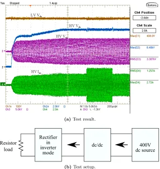
Recent technology advances in wide bandgap semiconductor devices such as SiC MOSFET enables the new developments of higher efficiency and smaller volume SST. The properties of SiC material such as wide bandgap, high-temperature stability and high saturated drift velocity make it highly suitable for the distribution SST[SA04]. Recently, a SST based on high voltage (>13kV) SiC MOSFET and JBS diode has been built [Wan13]. Tests carried out on this SST is only focused on standalone operations. and its performance under grid-connection needs to be studied.
Rectifier DC/DC Inverter
3.6kV grid 120V ac
(a)Test result.
Rectifier in inverter
mode
dc/dc 400V
dc source Resistor
load
(b) Test setup.
Figure 1.4 Test results of stand alone operation of Gen-2 SST.
1.3
Problems to be Solved
As mentioned in previous section, the Gen-1 SST lacks the potential ability to achieve higher conversion efficiency. With the new wide bandgap semiconductor devices, works has been done showing improved efficiency and simplified topology for high voltage operation. Nonetheless, further study on its grid-connected operation requires more attentions.
The research work presented in this proposal pushes one step forward toward the grid application of Gen-2 SST. To achieve this goal, following aspects are identified as the major topics:
1. Circuit components design for grid-connected operation;
For dc/dc stage, reactive power originated from extended ZVS range and high voltage link ripple will be studied.
2. Closed-loop controller for each stage;
The complete control strategy of SST consists of several layers based on the control contexts. The most top layer deals with energy and power management, whereas those lower layers directly interact with the converter hardware and protection gears. The goal of closed-loop control of SST is to provide a well-defined grid interface with fast dynamic response and good stability properties.
3. Gen-2 SST’s grid operation modes
This parts presents the extensive operation modes a grid-connected SST can perform regarding to power quality improvement and integration of renewable energy sources.
1.4
Outline
Chapter 2 focuses on the operation, design and control of ac/dc rectifier stage. First the steady state operating point is analysed with both ac phasor theory and linearization of dc voltage. The operational PQ diagram of the grid-connected SST is defined regarding to the current/voltage rating, generated losses and dc link voltage ripple. The capacitor sizing of high voltage dc link and ac side input filter are also presented.
A large portion of Chapter 2 will be devoted to the design of closed-loop controllers, i.e. the controller to regulate both dc link voltage and grid current. The overall structure for dc link voltage includes both a PI controller based on linearized dynamic dc voltage equation and a steady state model based feed-forward path that for dynamic response. The design of current regulation first examines three control scheme with different sensor locations. Impedance based analysis is proposed for the selecting of proportional gain used for both fundamental frequency current regulation and active damping.
Section 3 is about the dc/dc dual half bridge converter. It also starts with steady state trajectories of high frequency transformer’s different branch currents. Both active and reactive power’s relationship with voltage ratio and phase shift angle are derived and utilized to determine proper transformer parameters. For the control of DHB converter, a discrete time domain small signal model is derived based on different perturbations. A dual loop controller is then designed and verified with experimental result.
microgrid is built to demonstrate the SST’s ability to integrate different energy sources to supply local load.
CHAPTER
2
OPERATION AND CONTROL OF
2.1
AC/DC Rectifier Overview
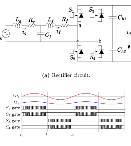
The circuit of rectifier stage and its modulation scheme are reproduced in Fig.2.1a and 2.1b, respectively. With 13kV MOSFET and JBS diode, a simple full bridge topology can be adopted for 3.6kV grid interface. In order to suppress the switching frequency harmonics, aLCLfilter is designed for its high attenuation ratio at frequencies above its resonant frequency fr. The
modulation scheme used is unipolar discontinuous pulse width modulation (DPWM). Current through the filter inductor are in continuous conduction mode.
(a)Rectifier circuit.
t0 t1 t2
vCf
iLf
S1gate S2gate S3gate S4gate
(b)PWM modulation.
Figure 2.1 Rectifier circuit and modulation.
2.2
Steady State Operation of Rectifier
2.2.1 Active and Reactive Power Limit
For grid-connected SST, it’s vital to define a safe operation area within which the required active/reactive power can be processed with enough margin of safety. Assume that the SST’s input filter is connected to a point of common coupling (PCC). The voltage of PCC is chosen as the phasor reference,e(t) =Esin(ωgt), where e(t) is PCC voltage’s time domain expression,
E and ωg are voltage amplitude and grid frequency respectively. If the phase lock loop (PLL)
is able to precisely track the phase angle of e(t), we can align the d-axis component to the amplitude,Ed=E. The active and reactive power flowing through the grid side filter inductor
Lg can be found as:
PP CC = IgdEd (2.1)
QP CC = IgqEd (2.2)
SP CC = IgEd (2.3)
where, PP CC, QP CC andSP CC are the active, reactive and apparent power out of PCC, Ed is the
d-axis component of PCC voltage,Igd andIgq ared- andq- axis current component ofig,Ig is
current amplitude.
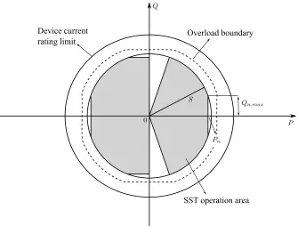
Since the semiconductor device is rated at 13kV 10A, the high voltage (HV) dc link voltage is selected at 6kV, which is about half of the break down voltage. The nominal ac input voltage is defined at 3.6kV such that the rectifier is operating at boost mode and final goal of 7.2kV can be achieved with series connection of the full-bridge. The power rating is defined based on nominal current, which is chosen with a peak value of 4A to achieve 10kW operation, Large current margin is preserved also considering that the current ripple at converter side inductor will be greater than the current in Lg. The proposed operating area of active/reactive power is
Device current rating limit
SST operation area Overload boundary
Figure 2.2 P-Q diagram.
To preserve the SST’s capability to provide 33% VAR compensation at nominal active power rating, the nominal apparent power representing the radius of the shaded area can be calculated as:
Pn = 10kW (2.4)
Qn,max = Pn0.33 = 3.3kW (2.5)
Sn =
q
P2
n+Qn,max = 10.53kV A (2.6)
The maximum current flowing out of PCC is therefore
Imax=
Sn
E = 4.14A
2.2.2 Steady State Operating Point
For ac systems, phasor analysis can be utilized to study the steady state operating point of each element’s current and voltage. The switching frequency harmonics can be ignored since it’s attenuated by theLCL filter. The dynamic equation will only focus on fundamental frequency by averaging all the physical dynamics over one sampling period, which is given as:
Lgdtd¯iLg = −Rg¯iLg+ ¯e−v¯Cf
Lfdtd¯iLf = −Rf¯iLf + ¯vCf −M¯(t) ¯vh
Cfdtdv¯Cf = ¯iLg −¯iLf
Chdtdv¯Ch = M¯(t) ¯iLf −¯iload
(2.7)
where ¯M(t) =da−db is the modulator signal of the H-bridge,da anddb are the duty ratio of
each of the H-bridge’s legs, respectively.Lg, Lf, Cf are the grid and converter side inductances
and filter capacitance;Rg,Rf are resistance of the two inductors, respectively; inductor currents
and capacitor voltages are selected as state variables. eis grid side voltage.
As can be seen, the averaged dynamic model of LCL rectifier is nonlinear due to the multiplication items ¯M(t)·¯iLf and ¯M(t)·v¯h. In order to derive the small signal model, we need
to linearize Equation (2.7) at nominal operating point (OP) first.
Equation (2.7) can be divided into an ac subsystemxac= [iLg, iLf, vCf]
T and a dc subsystem xdc= [vCh]. For the ac subsystem, the operating point is actually a group of sinusoidal trajectories
that can be characterized with phasors referred to grid voltage,~e=E∠0. Substitute the derivative operator with ω:
(RLg +ωLg)~iLg = ~e−~vCf
(RLf +ωLf)~iLf = ~vCf −M~v~ h
ωCf~vCf = ~iLg −~iLf
(2.8)
The derivation of operating points are based on given voltage and active/reactive power at PCC, whereby the grid side inductor current can be calculated as~iLg =Igd+Igq, withIgd=
P E
andIgq = QE. For filter capacitor and converter side inductor, Eq. 2.8 can be solved to find their
OP information:
~iLf = If d+If q
~vCf = Vf d+Vf q
~
m = Md+Mq
vh
where
If d = Igd(1−CfLgω2)−CfIgqRgωg
If q = Igq(1−CfLgω2g)−Cfω(E−IgdRg)
Vf d = E−Igd(Rg−ωgLg)
Vf q = −IgqRg−ωgLgIgd
Md = E(1−CfLfω2) +Igd ω2Cf(LfRg+LgRf)−(Rf +Rg)
+Igqωg(Lf +Lg) +IgqCfωg(RfRg−LfLgωg2)
Mq = Igd ω3CfLfLg−ω(Lf +Lg+CfRfRg)
+ωCfRfE
−Igq(Rg+Rf) +CfIgqωg2(LfRg+LgRf)
In order to find the OP of dc subsystem, the time domain expressions of control input m(t) and converter side inductor currentiLf are required:
iLf(t) = If dsin(ωgt) +If qcos(ωgt)
m(t) = Mdsin(ωt) +Mqcos(ωt) vh
(2.10)
Substitute Eq. 2.10 to the vCh state equation, we have
Chv˙h+
vh
Req
= 1 vh
If dMd+If qMq
2 +
If dMq+If qMd
2 sin(2ωt) +
−If dMd+If qMq
2 cos(2ωt)
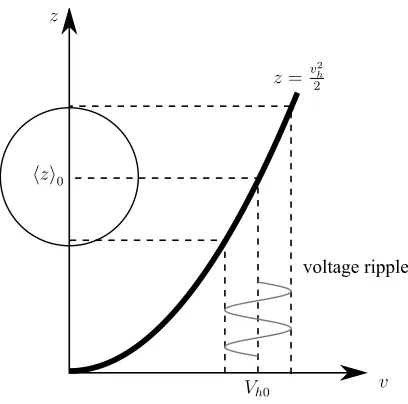
(2.11) Eq. 2.11 is a Bernoulli First-Order ODE with order of -1. It therefore can be linearized by introducingz= 12v2
h. Eq. 2.11 can be re-written as:
Chz0+
2 Req
z=Q1+Q2sin(2ωt) +Q3cos(2ωt) (2.12)
where
Q1 = If dMd+2If qMq Q2 = If dMq+2If qMd Q3 = −If dMd2+If qMq
(2.13)
Eq. 2.12 can be solved analytically with following solutions:
hzi0 = Req2Q1
hzi2 = ReqQ2+ChQ3R 2 eqω 2+2C2
hR2eqω2 sin(2ωt) +
ReqQ3+ChQ2R2eqω 2+2C2
hR2eqω2 cos(2ωt)
ztr(t) = −ZCe−
2t Req Ch
(2.14)
At steady state, item ztr(t) can be omitted and the HV link voltagevh(t) can be written as
vh,ss(t) =
p
2 (hzi0+hzi2(t)) (2.15)
Figure (2.3) verifies the derived OP of dc link voltage with simulation and experiment. The parameters for the test are E = 3600.Req= 8100Ω, Ch = 21µF. At 0.08s, the grid current’s
amplitude is regulated to 1.9A (ILg = 1.9) and the dc link voltage converges to its steady state
OP at a time constant of T =ChReq≈0.166s, which is approximate 10 grid cycles.
0 0.04 0.08 0.12 0.16 0.2 0.24 0.28 0.32 0.36 0.4 −8000
−6000 −4000 −2000 0 2000 4000 6000 8000
(a) Simulation. (b) Experiment.
Figure 2.3 Verification of the derived analytical results of dc link voltage withILg = 1.9. The
simu-lation plot shows the change ofp
2(hzi0+hzi2+ztr). Simulation result prior to 0.08s is omitted since
the model is not applicable to uncontrolled diode rectifier; The experiment result shows the change of dc link voltage when grid side current amplitude is regulated at 1.9A, starting at 0.08s.
2.3
Design of Passive Components
2.3.1 Selection of HV Link Capacitance
for the sake to reduce required capacitance, however, additional complexity in control and measurement will also increase cost. It’s therefore to study the system operating including the voltage ripple, P-Q capacity and filter losses together to find a minimum capacitor value which can meet all constraints.
voltage ripple
Figure 2.4 DC ripple relationship betweenzand v.
From the relationships of filter current and voltage, following circuit operation parameters are able to be analysed
• Active and reactive power from PCC; • dc link voltage ripple;
• Filter losses;
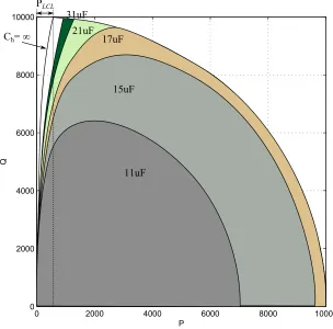
With the introduction of z =v2/2, the dc link voltage ripple can be transferred to z, as shown in Fig. 2.4. The analytical solution of z is derived in Eq. 2.14 in previous section. Its relationship with PCC current and voltage with given maximum apparent power are plotted in Fig. 2.5.
Fig. 2.5 illustrates the relationship between dc voltage ripple (half of peak-peak value), active/reactive power from PCC and differentCh values. The voltage ripple limit is set to a
100 P (kW) 10 Q (kvar) 10 0 2 0 4 6 8 2 4 6 8 DC rippl e (V) 0
(a) Ch= 11uF
100 P (kW) 10 Q (kvar) 10 0 2 0 4 6 8 2 4 6 8 DC rippl e (V) 0
(b)Ch= 17uF
100 P (kW) 10 Q (kvar) 10 0 2 0 4 6 8 2 4 6 8 DC rippl e (V) 0
(c) Ch= 21uF
100 P (kW) 10 Q (kvar) 10 0 2 0 4 6 8 2 4 6 8 DC rippl e (V) 0
(d)Ch= 31uF
0 2000 4000 6000 8000 10000 0
2000 4000 6000 8000 10000
P
Q
11uF 15uF 17uF 21uF 31uF
Ch= ∞
PLCL
P-Q plane with different dc link capacitance values. With the increase of Ch, for a given dc
link voltage ripple and maximum apparent power, the reachable region is also increased. Such increase will become saturated whenCh becomes large, which is obvious in Fig. 2.6 that from
21uF onwards the increased area is relatively small, compared whenCh is small. In theory, the
maximum region occurs when the dc link capacitance is infinity, which has a left boundary that represents the losses caused by theLCL filter, annotated as theCh=∞. For filter inductors
with large resistance, the Ch =∞curve will shift towards right, reducing the maximum reactive
power when active power is small.
2.3.2 LCLFilter Design
For grid-connected operation, the harmonics that allowed to be injected into the grid is strictly limited by various grid codes, such as IEEE. In order to design the grid interface filter, first the harmonics source should be identified and its effect on current waveform be analysed. The design procedure consists of two steps: first, the current ripple introduced by the switching of the H-bridge will be examined in time domain regarding to the specific modulation scheme adopted. This will show the maximum current ripple the filter inductor will handle. Next, based on the transfer function of the filter, grid side inductor can be calculated with given ripple occurrence.
• Filter capacitor based on reactive power flowing through; • Converter side inductor design for given current ripple; • Grid side inductor based on filter transfer function;
Figure 2.7 DC ripple relationship betweenzand v.
Capacitor can be calculated based on the reactive power introduced by theCf is at 2% rated
power, which yields:
QCf = 200var= 3600 2ω
gCf (2.16)
To study the differential mode harmonics introduced by SST, the grid side voltage is ignored and the circuit is shown as Fig. 2.7. With single frequency unipolar PWM, as shown in Fig. 2.1b, the converter side inductor time domain analysis of current ripple on filter inductor. Peak to peak ripple:
(a)Ripple current caused by PWM voltage.
1
0
-1
Curr
ent (A)
0 π 2π
(b)Simulated ripple current.
Figure 2.8 Ripple current in converter side inductor.
∆if,pp(t) =
TSWVdc
Lf
(1−m(t))m(t) =TSWVdc
Lf
(1−Msin(ωgt))Msin(ωgt) (2.18)
where M is modulation signal amplitude, ωg is grid frequency and TSW is switching period,
∆if,pp(t) is peak to peak current ripple in converter side inductorLf. As can be seen, maximum
current ripple occurs when the derivative of Eq. 2.18 is zero: d
dt∆if,pp(t) = ωgcos(ωgt)(1−2Msin(ωgt)) = 0 (2.19) (2.20)
we can find the maximum current ripple and its phase angle:
∆if,ppmax =
TSWVdc
4Lf
(2.21)
θ∆i,ppmax = arcsin(
1
For the 3.6kV SST, with M = 36006000√2 = 0.85, the maximum current ripple can be calculated as:
θ∆i,max= arcsin(
1
2×0.85) = 0.629 = 36
◦ (2.23)
For a maximum peak-to-peak ripple current of 50% (-25%, 25%) of fundamental current, which is ∆if,pp(t) = 2A, at givenTSW,Vh0, the minimum value of converter side inductance can be found as:
Lf ≥
TSWVdc
∆if,max
(1−0.85 sin(0.629)) 0.85 sin(0.629) = 0.125H (2.24)
ωres =
s
Lf +Lg
CfLfLg
(2.25)
ωres2 = Lf +Lg CfLfLg
(2.26)
Lg+Lf = ω2resCfLfLg (2.27)
the resonant frequency ωres is referred to switching frequency by:
ωres=kωSW (2.28)
Frequency domain analysis of the pwm harmonics in grid side yields the transfer function from converter side voltagevpwm(s) to grid side currentig(s):
iL(s)
vpwm(s)
= 1−CfLgs
2
CfLfLgs3+ (CfLfRg+CfLgRf)s2+ (CfRfRg+Lf+Lg)s+Rf+Rg
(2.29)
ig(s)
vP W M(s) = −
1
CfLfLgs3+ (CfLfRg+CfLgRf)s2+ (CfRfRg+Lf+Lg)s+Rf+Rg(2.30) at switching frequency, the reactance will be much greater than resistance therefore all the resistance values can be omitted:
iL(s)
vP W M(s)
s=jωSW
≈ ω 1
SWLf
(2.31)
ig(s)
vP W M(s)
s=jωSW
≈ 1
CfLgLfωSW|ω2res−ωSW2 |
(2.32)
ig(s)
Set the grid side current ripple to be 10% of filter inductor current, the grid side inductor of LCL filter can be found:
1
CfLg|ωres2 −ωSW2 |
= 10% (2.34)
Lg= 0.19H (2.35)
When building the grid side filter inductor, headroom should be reserved for grid impedance, therefore the actual grid side inductor value can be selected smaller than calculated value. In the SST hardware, the leakage inductor of step-up transformer is used which have a inductance of 0.17H.
2.3.3 Filter Losses
The losses of the LCLfilter are mostly caused by the inductors,Lg and Lf. The ESR or loss
tangent of the filter capacitor is very small on operating frequency therefore losses on capacitor can be omitted. For magnetic components,
Ploss,acf ilter = Ploss,Lg +Ploss,Lf (2.36)
Ploss,Lg = Pres,Lg +Pcore,Lg (2.37)
Ploss,Lf = Pres,Lf +Pcore,Lf (2.38)
(2.39)
Since the current ripple in grid-side inductor is much smaller than in converter-side inductor, it can be ignored when calculating theRMS current going through grid-side inductor, therefore the resistive winding loss of grid-side inductor can be found as:
Pres,Lg =I 2
RM S,LgRg (2.40)
Due to the existence of relative large current ripple, the RMS current in converter side inductor will be greater than grid side inductor. [KK] presents an analytic solution for the calculation of ripple current’s RMSvalue:
IRM S,Lf ,rip = TSWVh0
2Lf
r
M4
8 −
8M3 9π +
M2
6 (2.41)
side inductor can be calculated as:
IRM S,Lf =qI2
RM S,Lg +I 2
RM S,Lg ,rip (2.42)
and resistive loss:
Pres,Lf = (IRM S,Lg2 +IRM S,Lg ,rip2 )Rf (2.43)
= IRM S,Lg2 +T 2 SWV
2
h0 4L2
f
M4
8 −
8M3 9π +
M2 6
!
Rf (2.44)
With designed parameters, the total winding loss of the LCLfilter can be found as 330W at nominal load. Most of the losses (230W) is contributed by the excessive resistance found in the step-up transformer. Losses by converter side inductor is composed of fundamental current (93W) and ripple current losses (10W).
2.4
DC Link Controller
DC link voltage controller is the outermost loop for rectifier’s converter control diagram. The dc voltage is sustained as a sign of balance between grid side active power and load. The said SST is a single phase with sinusoidal voltage and current at ac side, the instantaneous active power and reactive power are dc biased with superposition of 120Hz ripples. The analytical expression of dc voltage in terms of grid active/reactive power is presented in Chapter 2.
The first order dynamic equation of linearized dc link voltage is:
Chz0+
2 Req
z=Q1 (2.45)
where
Q1 =
If dMd+If qMq
2
If d = Igd(1−CfLgωg2)−CfIgqRgωg
If q = Igq(1−CfLgωg2)−Cfωg(E−IgdRg)
Md = E(1−CfLfωg2) +Igd ω2gCf(LfRg+LgRf)−(Rf +Rg)
+Igqωg(Lf +Lg) +IgqCfωg(RfRg−LfLgω2g)
Mq = Igd ω3gCfLfLg−ωg(Lf +Lg+CfRfRg)+ωgCfRfE
replaced by their reference value, also assume that at fundamental frequencyIgd≈If d,Md≈Ed
and dc link voltage’s dc component is unrelated toIgq sinceMq≈0. With the output of voltage
loop as the current referenceIgd∗ , we have the closed-loop transfer function from voltage reference z∗ toz:
Chz0+
2 Req
z=E (Kp+
Ki
s )(z∗−z)
2 (2.47)
the closed-loop transfer function from z∗ tozis then z
z∗ =
E(Ki+Kps)
2Chs2+ (R4eq +KpE)s+EKi
(2.48)
The transfer function ratio at dc is unity. The natural frequency and damping factor are calculated as:
σ = 4
Req +EKp
2√2ChEKi
ωn =
r
EKi
2Ch
(2.49)
Eq. 2.49 will be used to tune the value of PI controller parameters. In order to have fast dynamics, the dc energy equation at steady state is
hzi0=Req
If dMd+If qMq
4 (2.50)
substitute Eq. 2.46 into Eq. 2.50 and assumeRg, Rf are negligible, the small signal relationship
betweenhzi0 and Igd can be calculated as:
∂hzi0 ∂Igd
= Req E CfLfω 2−1
CfLgω2−1+CfE ω ω (Lf +Lg)−CfLfLgω3
4
(2.51) moveReq to the left side and representz withVdc:
Idc
∂Vdc
∂Igd
= E CfLfω 2−1
CfLgω2−1
+CfE ω ω (Lf +Lg)−CfLfLgω3
4 (2.52)
∆Igd =
4∆VdcIdc
Ed
As a feed-forward item, we can have
Igd,k = Igd,k−1+ ∆Igd
= Igd,k−1+
4∆VdcIdc,k
Ed
= Igd,k−1+
4(Vdc,k−Vdc,k−1)Idc,k
Ed
(2.54)
This is a discrete integration function with voltage difference as input and a varying gain of 4Idc,k
Ed
.
The overall controller structure for dc link voltage is shown in Fig. 2.9.
Vdc k 4Idc k
Ed
1 s Vdc k−1
z∗ Kp+Ki
s I
∗
gd
z +
−
+ +
−
+
Figure 2.9 Diagram forVdccontrol.
2.5
Selection of Current Control Scheme
2.5.1 Impedance Based Analysis
For power supply of both current and voltage types, although the output can be regulated within its bandwidth, it inevitably will have small disparity between actual output and reference that is caused by loading condition. The reason for this is that the closed-loop transfer function from reference to actual output include disturbance item that function as internal impedance. Such item’s frequency response can be measured via frequency analyser and be examined carefully. Otherwise, they will display a regulation error while load has large range or even cause instability when multiple converters are interconnected.
In order to apply, the ac parameters are first transformed into dq synchronous reference frame and become dc, then small perturbation are added to study the small signal stability.
In systems where multiple inverters share a common bus, impedance shaping techniques are deployed for load sharing and harmonic rejection. This eliminates the requirement of central coordinate unit while provide easier integration for systems such as Microgrid, distributed generation, etc.. Many times, such study on output impedance of inverter systems don’t require reference frame transformation. Instead, the fast switching actions are averaged during one switching period, and the circuit itself is considered a linear system for direct derivation of transfer function. AC variables then are signals of particular frequency.
The final form of a current mode inverter is shown in Fig. 2.10. It’s similar to a current source’s Nortan equivalent circuit, composed by an ideal sourceIo(s) in parallel with an output
impedanceZo(s). The goal of regulation is to have Io very close to reference and Zo to infinity.
Io(s) Zo(s)
Ig(s)
Figure 2.10 Equivalent current source with output impedance of current mode inverter.
2.5.2 Impedance Formulation of Current Control Schemes
Single phase grid interfaced rectifier withLCLfilter is shown in Fig. 2.11. For rectifier operation, the outer loop controller regulates dc bus voltage to be constant and the inner loop is current controller. Based on the placement of current sensor, different current can be selected as control subject. Following section derives the Norton equivalent impedance representation of three current control schemes, namely, grid side current control, both grid side and converter side current control, grid side and filter capacitor current control. The reason for keeping a Ig for all
Figure 2.11 Current mode grid connected rectifier with LCL filter and its equivalent circuit.
The equivalent Norton circuit will replace the converter bridge and the LC filter on its side. The grid side inductor is excluded from the equivalent circuit. Therefore the output impedanceZo will be seen as in parallel with lumped grid impedanceZg, as shown in Fig. 2.11’s
bottom diagram. The grid background voltage can be excluded from the analysis since it can be compensated with feedforward measurement of filter capacitor voltage.
2.5.2.1 Grid Side Current Controller
The control diagram of grid side current regulation is depicted in Fig. 2.12. Here, only the grid current is measured and compared with reference current. Controller transfer function Gi(s)
can be either a PI or PR controller. Converter gain is simplified as the constant dc voltageVdc.
The closed-loop transfer function from current reference Ig∗ to converter side inductor current If
can be derived as Eq. 2.55. Converter is simplified as a constant gain of dc voltageVdc. The dc
voltage is considered as the base value for PU representation so is omitted in further equations.
I∗
g Gi(s) Vdc sL1f
1 sCf
Ig(s)
+ + − +
− −
VCf(s)
If =
CfGiGpwms
CfLfs2+CfRfs+ 1
Ig∗− CfGiGpwms−1
CfLfs2+CfRfs+ 1
Ig (2.55)
The filter capacitor voltage is therefore
VCf =
If −Ig
sCf
(2.56)
= GiGpwm
CfLfs2+CfRfs+ 1
Ig∗− Rf +Lfs+GiGpwm
CfLfs2+CfRfs+ 1
Ig (2.57)
The components of Norton equivalent circuit are derived as:
Io(s) =
GiGpwm
Rf +Lfs+GiGpwm
Ig∗ (2.58)
Zo(s) =
Rf +Lfs+GiGpwm
CfLfs2+CfRfs+ 1
(2.59)
The output impedance Zo is in parallel with grid impedanceZg, this paralleled impedance
Zg will indicate the resonant frequency of overall system. With this control scheme, the parallel
impedance can be found as:
Zp = Zo||Zg
=
Rf +Lfs+Gi
CfLfs2+CfRfs+ 1
||(Lgs+Rg)
= Lgs(Rf +Lfs+Gi)
Rf+Lfs+Lgs+Gi+CfLfLgs3+CfLgRfs2
(2.60)
There are two frequency ranges at interest. First is the fundamental frequency at 60Hz, the transfer function fromIg∗ toIg should be close to 1 and Zo should be as large as possible. The
other frequency range is higher frequency around the resonant frequency of Zo||Zg. In order
to have a valid representation with continuous model, this resonant frequencyωres should be
below Nyquist frequency. IfGi doesn’t include a high pass filter such as derivative item, then at
higher frequency its gain is very small and can often be neglected. In addition, the loneRf in
the denominator can be neglected, however the Rf in itemCfLgRfs2 needs to be kept for the
large value of s2. With these simplifications, we have
Zp ≈
LgLfs
CfLfLgs2+CfLgRfs+ (Lf +Lg)
If we further assume that Rf = 0, then the paralleled impedance can approximated as
Zp ≈
LfLgs
CfLfLgs2+Lf +Lg
(2.62)
the resonant frequency can be found by solving
CfLfLgs2+Lf +Lg = 0 (2.63)
we have
s = ±j
s
Lf +Lg
CfLfLg
ωres =
s
Lf +Lg
CfLfLg
(2.64)
In the simplified form shown in Eq. 2.62, no damping factor in the system and it become unstable with dynamic disturbance. A damping factor, however, can be added to the system if assumption to neglectRf is no longer applied. This can be seen in Eq. 2.59 whereCfLgRf provides damping
to the second order system dynamic equation. Physically increased Rf can increase damping
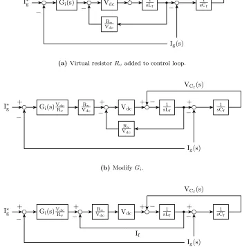
factor but is not a good practice since extra loss will be dissipated by the resistor. An approach called Virtual Resistor was proposed by emulating a resistor in the inverter’s control loop. It’s usually implemented that the calculated modulation signal will subtract the product of filter current and a constantRv before it’s sent to PWM generator, as depicted in Fig. 2.13a.
The roots of characteristic equation with Rv can be calculated as:
s = σ±jω
= − Rv 2Lf ±
j
s
1 CfLfLg
Lf +Lg−
CfLgR2v
4Lf
(2.65)
Eq. 2.65 shows that the damping factor of parallel impedanceZp is determined by the ratio of
filter inductor’s resistanceRf and inductance Lf. The damping ratio with virtual resistor Rv is
ξ= Rv 2ωresLf
I∗
g Gi(s) Vdc sL1f
1 sCf
Rv
Vdc
Ig(s)
+ + + +
−
−
− −
VCf(s)
(a)Virtual resistorRv added to control loop.
I∗g Gi(s)VRdcv VRdcv Vdc sL1f
1 sCf
Rv
Vdc
Ig(s)
+ + + +
−
−
− −
VCf(s)
(b)ModifyGi.
I∗
g Gi(s)VRdcv VRdcv Vdc sL1f
1 sCf
Ig(s)
+ + + +
−
If
−
− −
VCf(s)
(c) Transformed control diagram which shows the inclusion ofRvis equivalent to add an inner
current loop of filter inductor currentIf.
Figure 2.13 The control diagram with virtual resistorRv and its equivalent structure with dual loop
current control.
2.5.2.2 Ig andIf Current Controller
As Fig. 2.13 shows, the active damping approach by adding a virtual resistor can improve the system damping to dynamic disturbances. Essentially, what the virtual resistor does is to include an inner current loop with filter inductor current If feedback. It will not only effect damping
fundamental one. In this section, the control scheme with both Ig and If feedback will be
converted to Norton equivalent circuit to extract output impedance. The control diagram is depicted in Fig. 2.14.
I∗
g Gii1(s) Gii2(s) Vdc sL1f
1 sCf
Ig(s)
+ + + +
− −
If(s)
Ig(s)
− −
VCf(s)
Figure 2.14 Diagram forIg outer loop andIf inner loop control.
The loop equation of filter inductor current ILf can be solved and represented by current
reference Ig∗ and grid side currentIg:
ILf(s) =
CfGii1Gii2s
CfLfs2+ (Rf +Gii2)Cfs+ 1
Ig∗− CfGii1Gii2 s−1
CfLfs2+ (Rf +Gii2)Cfs+ 1
Ig (2.67)
The output voltage across capacitor can be found as
VCf(s) =
ILf(s)−Ig(s)
sCf
= Gii1Gii2
CfLfs2+ (Rf +Gii2)Cfs+ 1
Ig∗− Rf+Lfs+Gii2 +Gii1Gii2 CfLfs2+ (Rf +Gii2)Cfs+ 1
Ig
(2.68)
And the components of Norton equivalent circuit are:
Io =
Gii1Gii2
Rf +Lfs+Gii2 +Gii1Gii2
Ig∗ (2.69)
Zo =
Rf +Lfs+Gii2 +Gii1Gii2 CfLfs2+ (Rf +Gii2)Cfs+ 1
The parallel impedance is:
Zp(s) = Zo(s)||Zg(s)
= (LfLg) s 2+ (L
g (Rf +Gii2+Gii1Gii2) +LfRg) s
(CfLfLg) s3+ (CfLfRg+CfLgRf +CfGii2Lg) s2
+Rg (Rf+Gii2+Gii1Gii2)
+ (Lf +Lg+CfRfRg+CfGii2Rg)s+Rf +Rg+Gii2+Gii1Gii2
(2.71)
We can simplifyZp by neglectingRg and Rf:
Zp(s)≈
LfLgs2+sLgGii2(1 +Gii1)
CfLfLgs3+CfLgGii2s2+ (Lf +Lg)s+Gii2(1 +Gii1)
(2.72)
Again, two frequency ranges need to be considered:
At low frequency range around fundamental frequency, the gain of outer loop controller Gii2 needs to be very large that Eq. 2.72 in low frequency range can be approximated to
Zp,LF(s)≈
sLgGii2(1 +Gii1) Gii2(1 +Gii1)
=sLg (2.73)
which means that Zo is almost an open circuit, with little effect on the transfer function from
Ig∗ toIg, which can be considered unity.
At high frequency range, in order to incorporate damping into Zp,Gii1 should have a gain of −1. Assume that
Gii1,HF =−1 (2.74)
the parallel impedance at high frequency can be simplified as:
Zp,HF(s)≈
LfLgs
CfLfLgs2+CfLgGii2s+ (Lf +Lg)
(2.75)
In this high frequency expression of Zp, inner loopGii2 shall have a large gain to provide damping. This is often achieved by assigningGii2a constant value to make it frequency-insensitive. The value of Gii2 can be determined by Eq. 2.75’s poles:
s = σ±jω
= −Gii2 2Lf ±
j
v u u t
4L2f + 4LgLf−CfLgG2ii2 4CfLgL2f
Both the low frequency and high frequency requirements on Gii1 can be fulfilled with a parallel structure including a low frequency range controller and a high frequency pass filter, as shown in Fig. 2.15. At fundamental frequency, Gii1,LF is expected to have a high gain whereas
around resonance frequencyGii1,HF needs to provide a gain of−1. The coupling among them
depends on their respective frequency selectivity. Improving such frequency selectivity has been a research topic of many publications. Although their effectiveness, the process involves signal processing and requires carefully selected parameters.
Gii1;HF
Ig(s)
I∗
g Gii1;LF Gii2(s) Vdc sL1f
1 sCf
Ig(s)
+
+ + + + +
− −
If(s)
− −
VCf(s)
Figure 2.15 Parallel structure ofIg outer loop controllerGii1.
Gii1,LF and Gii1,HF can be decoupled if, instead of filter inductor current If, the filter
capacitor currentICf is measured for the inner loop. The reason for this is explained in Fig. 2.16
where the path for high frequency current is extracted to an equivalent diagram with ICf
feedback. The outer loop controller now only has low frequency range partGii1,LF left. The
design ofGii1 is much simpler as it only concerns increasing the gain at fundamental frequency. However, the implementation of Gii1,LF will always include a proportional path, which will
−1 I∗
g Gii1;LF(s) Gii2(s) Vdc sL1f
1 sCf
Ig(s)
+
+ + + +
− −
If(s)
Ig(s)
− −
VCf(s)
(a) At high frequency range,Gii1,HF =−1. It’s assumed thatGii1,LF has large attenuation and is
considered an open path at high frequency range.
Ig(s)
I∗
g Gii1;LF(s) Gii2(s) Vdc sL1f
1 sCf
Ig(s)
+
+ + + +
− −
If(s)
Ig(s)
− −
VCf(s)
(b) Ig∗has only fundamental frequency item therefore only−Ig is multiplied with−1 and added to the
output ofGii1,LF.
I∗
g Gii1;LF(s) Gii2(s) Vdc sL1f
1 sCf
Ig(s) ICf(s)
+ + + +
− −
Ig(s)
− −
VCf(s)
(c) CombineIg(s)−If(s) into−ICf(s). The modified controller is equivalent to a inner loop regulating filter capacitor current.
Figure 2.16 The decoupling of outer loop controllerGii1is achieved by changing the feedback item
fromIf toICf for inner loop.
2.5.2.3 Ig andICf Current Controller
I∗g Gi1(s) Gi2(s) Vdc sL1f
1 sCf
Ig(s)
+ + + +
− −
ICf(s)
Ig(s)
− −
VCf(s)
Figure 2.17 Diagram forIg outer loop andICf inner loop control.
The closed-loop transfer function fromIg∗ andIgto filter inductor currentIf can be calculated
as:
If(s) =
CfGi2s−CfGi1Gi2s+ 1 CfRfs+CfLfs2+CfGi2s+ 1
Ig+
CfGi1Gi2s
CfRfs+CfLfs2+CfGi2s+ 1
Ig∗ (2.77)
Voltage across the filter capacitor can be calculated:
VCf =
If −Ig
sCf
= Gi1Gi2
CfRfs+CfLfs2+CfGi2s+ 1
Ig∗− Rf +Lfs+Gi1Gi2 CfRfs+CfLfs2+CfGi2s+ 1
Ig
(2.78)
Re-write Eq. 2.78 in Norton form VCf =Zo(Io−Ig) and we have:
Io(s) =
Gi1Gi2 Rf +Lfs+Gi1Gi2
Ig∗ (2.79)
Zo(s) =
Rf +Lfs+Gi1Gi2 CfLfs2+ (Rf +Gi2)Cfs+ 1
(2.80)
The outer loop controller Gi1’s major focus is to regulate Ig to follow Ig∗ at fundamental
After connected to grid, the overall parallel impedance Zp is
Zp(s) = Zo(s)||Zg(s)
= (LfLg)s 2+ (L
g (Rf +Gi1Gi2) +LfRg) s
(CfLfLg) s3+ (CfLfRg+CfLgRf +CfGi2 Lg) s2
+Rg (Rf +Gi1Gi2)
+ (Lf +Lg+CfRfRg+CfGi2 Rg) s+Rf +Rg+Gi1Gi2
(2.81)
Assume that at high frequency range, Gi1 << 1 and also neglect Rg and Rf, Zp can be
simplified as:
Zp,HF(s)≈
LfLgs
CfLfLgs2+CfGi2 Lgs+ (Lf +Lg)
(2.82)
The roots of characteristic equation are
s = σ±jω
= −Gi2
2Lf ±
j
s
Lf +Lg
CfLgLf −
G2
i2 4L2
f
(2.83)
Eq. 2.83 shows that the inner loop controller Gi2(s)’s main purpose is to damp the overall system at high frequency range.
2.5.3 Selection of Current Controller
The previous three subsections derived the Norton Equivalent form of different Ig control
structures. By finding the current source output impedance Zo, overall parallel impedanceZp,
the function provided by each loop controller can be identified. Their suitability to achieve both fundamental frequency tracking and high frequency damping are then examined.
For controllers with only Ig regulation, it’s difficult to directly apply active damping without
adding extra current feedback. With If as the new feedback, a virtual resistor can be included
in the loop to provide damping by emulating a large resistor in series with filter inductor. It’s then shown to be equivalent to control scheme withIg outer loop and If inner loop.
The impedance model of Ig outer loop and If inner loop scheme indicates that to achieve
component.
The SST’s rectifier stage will then choose Ig outer loop and ICf inner loop as its current
controller. The large gain at fundamental frequency will be achieved by resonant controller tuned with increased bandwidth. The inner controller Gi2 will be a constant. The design procedure for dc voltage outermost loop,Gi1 and Gi2 parameter selection are presented in next section.
2.6
Design of Current Controller
2.6.1 Resonant Controller and Its Digital Implementation
In order to fulfil the harmonic compensation, it’s difficult to expand control bandwidth by PI controller. Reference-frame transformation onto all possible frequencies are computation intense for real-time processors to finish. Therefore PR controller with low pass filter is adopted here for its high gain at particular frequency. The idea of PR controller is to have theoretically infinite gain at particular frequencyωr. This is achieved by controller transfer function:
Gr(s) =
s s2+ω2
r
(2.84)
Fig. 2.18 shows the bode plot of Eq. 2.84. Since the denominator will become infinite small atωr, its gain will increase at a very narrow frequency range. Such selectivity is not easy for
practical implementation, especially for digital controller to implement. An alternative is to add a damping factor ξ at the denominator, as shown in Eq. 2.85. This method is similar to connect the resonant controller to a low pass filter. The gain atωr is reduced as the denominator
−20 0 20 40 60
Magnitude
(dB)
59.7 59.8 59.9 60 60.1 60.2 60.3
−180
−90 0 90 180
Phase
(deg)
Bode plot of pure resonsnt controller
Figure 2.18 Bode plot of a pure resonant controller. The magnitude gain is large in a very narrow frequency range. A discontinuous transition from 90◦ to −90◦ when frequency crossesω
r.
G(s) =Kr
s s2+ 2ξω
rs+ωr2
(2.85)
The bandwidth of low pass filter resonant controller in Eq. 2.85 is implied by the enlarged frequency range where transfer function gain is larger than 0db,BWr= [ωr−ωc, ωr+ωc]. For
grid interfaced inverters, the frequency range is kept within a small range which helps to define theBWr. After determining bandwidth, the gainKr can be calculated by phase margin (P M)
at frequency ωr−ωc orωc+ωc. In the pure resonant transfer function Eq. 2.84, the phase plot
has a sharp turning point at resonant frequency. After the inclusion of damping factorξ, this transition can be smoothed, with the downplay of transfer function gain. Such relationship can be exploited by changing the phase margin at the pre-defined crossover frequencyωr−ωc. Gain
Kr can then be calculated with this phase margin equation.
ξ = tan(P M−90◦)ω 2
r −(ωr−ωc)2
2ωr(ωr−ωc)
(2.86)
Kr = p ωr−ωc
(ω2
r−(ωr−ωc)2)2+ (2ξωr(ωr−ωc))2
(2.87)
Table 2.1 Resonant controller parameters
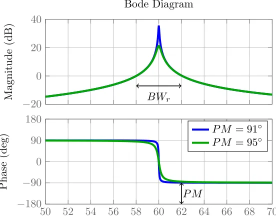
BWr = [58,62]Hz ξ Kr Max gain
P M = 91◦ 0.00059 25.56995 35.163 dB (57.3) P M = 95◦ 0.00297 25.6637 21.194 dB (11.5)
−20 0 20 40
BWr
Magnitude
(dB)
50 52 54 56 58 60 62 64 66 68 70
−180
−90 0 90 180
P M
Phase
(deg)
P M = 91◦ P M = 95◦ Bode Diagram
Figure 2.19 Envelope ofRg andLg estimation range with different PLL resolution. Perturbation
reactive power is ∆Q= 1kvar.
To implement Eq. 2.85 in a digital controller, we need to transform it to discrete expression that is easy to realize. Eq. 2.88 shows that it can be re-written in a form similar to the gain of closed-loop path. The item ωr
s is the gain of forward path and ωr
s + 2ξ represents the feedback
gain.
G(s) = Kr
ωr
s
1
ωr
1 +ωr
s (ωsr + 2ξ)
= Kr ωr
ωr
s
1 +ωr
s (ωsr + 2ξ)
u ωr s
Kr
ωr
y
ωr
s
2ξ
+ A D B
+
C
+
−
Figure 2.20 Double integrator implementation of large bandwidth resonant controller.
Its control diagram is then equivalent to a feed-back system, as shown in Fig. 2.20. This double integrator structure can greatly reduce the complexity of digital implementation.
With Tustin approximation, we can substitute s= T2
s
z−1
z+1 in Eq. 2.88. The forward path from AtoD can be transformed to discrete form:
D = Aωr s = ATωr
s 2
z−1
z+1
= ωrTs 2
z+ 1
z−1A (2.89)
D(k) =D(k−1) +ωrTs
2 (A(k) +A(k−1)) (2.90)
0.08 0.09 0.1
−1 0 1
Continuous Digital
0.08
0.09
0.1
−
1
0
1
Continuous
Digital
Figure 2.21 Comparison between continuous-time model and discrete model of resonant controller.
Fig. 2.21 depicts the waveform after a sinusoidal input signal u= sin(ωrt) passes through
modelled resonant controller in both continuous-time and discrete domains. The resonant controller has a bandwidth from 58Hz to 62Hz and phase margin of 91◦. The digital sampling frequency is 12k Hz,Ts= 121k. The zoomed area shows that the digital implementation given in
List.2.1 can provide good agreement with original model.
Listing 2.1 Digital implementation
1. kth sampling, update U(k)
2. A(k) =U(k)−B(k−1)−C(k−1)
3. D(k) =D(k−1) +ωrTs
2 (A(k) +A(k−1))
4. B(k) =B(k−1) +ωrTs
2 (D(k) +D(k−1))
5. C(k) = 2ξD(k)
6. y(k) = Kr ωr
2.6.2 Active Damping at High Frequency 2.6.2.1 Kp’s Impact on Active Damping
Resonant controller can provide large gain at fundamental frequency. However, its phase angle will decline from 90◦ to −90◦ sharply after resonant frequency is surpassed. This will pose potential for performance degradation because of reduced phase margin. Later on, it’s shown that adding a proportional pathKp will effectively prevent such cause. This modifiedGi1 is now Proportional Resonant (PR) controller. Although it may improve low frequency regulation, the newly introduced parallelKp path will nevertheless increase the coupling between low frequency
and high frequency responses. In this subsection,Kp’s effect on high frequency current will be
examined.
Kp
I∗
g Gi1;Res Gi2 Vdc sL1f
1 sCf
Ig;HF+LF
Ig +
−Ig;HF
+
+ + IHF + +
− −
ICf;HF+LF
− −
VCf
(a)Path for high frequency current feedback.
Kp
I∗g Gi1;Res Gi2 Vdc sL1f
1 sCf
Ig;LF
Kp
If;HF
−
1−Kp −
+
+ + + IHF + + −
ICf;HF
ICf;LF
−
Ig
− −
VCf
(b) Equivalent high frequency current path.
Figure 2.22 High frequency current path withKp in parallel with resonant controllerGi1,res.


![Fig. 2.19 depicts two low pass resonant controllers’ bode plots. The bandwidth for both are�[58, 62]Hz with phase margin of 91◦ and 95◦](https://thumb-us.123doks.com/thumbv2/123dok_us/1305540.1163189/49.612.179.455.78.294/fig-depicts-resonant-controllers-plots-bandwidth-phase-margin.webp)