ABSTRACT
ISIK, SEMIH. Investigation of the Operation of MMC Based Point to Point HVDC System with Feed-forward Current Control Scheme (Under the direction of Dr. Subhashish Bhattacharya).
Investigation of the Operation of MMC Based Point to Point HVDC System with Feed-forward Current Control Scheme
by Semih Isik
A thesis submitted to the Graduate Faculty of North Carolina State University
in partial fulfillment of the requirements for the degree of
Master of Science
Electrical Engineering
Raleigh, North Carolina 2018
APPROVED BY:
_______________________________ _______________________________ Dr. David Lubkeman Dr. Mesut Baran
_______________________________ Dr. Subhashish Bhattacharya
ii
DEDICATION
iii
BIOGRAPHY
iv
ACKNOWLEDGMENTS
First and foremost, I would like to express my sincere appreciation to my advisor, Dr. Subhashish Bhattacharya for offering me the opportunity to pursue my education at the great place FREEDM (Future Renewable Electric Energy Delivery and Management) systems center with amazing people at NC State University. His endless support, very deep knowledge, large industry and academic network and constructive comments allowed me to finish M.Sc., successfully.
Second, I am very honored and thankful to have Dr. David Lubkeman and Dr. Mesut E. Baran in my committee.
I appreciate the presence and friendship of all students and employees of FREEDM. My special “thank you” goes to my teammate Mr. Mohammed Alharbi for helping me throughout the lab setup and testing.
I am very grateful to have Turkish Student Association members at NC State for their support and great friendship. I am also truly blessed to have Zorica and Stefan Sandor, who are like my mom and dad in the USA.
I am truly grateful to my parents and sister for the relentless support, and great motivation not only during my masters but also throughout my life.
v
TABLE OF CONTENTS
LIST OF TABLES ... vii
LIST OF FIGURES ...viii
Chapter 1 Introduction ... 1
1.1. Statement of problem ... 1
1.2. Thesis Objective ... 1
Chapter 2 Topology Evaluation ... 3
2.1. Voltage Source Based Conventional Converters ... 3
2.2. VSC Based Modular Multilevel Converter (MMC) ... 5
Chapter 3 Modular Multilevel Converter (MMC) ... 7
3.1. Structure of MMC ... 7
3.2. Modelling and operation of single and three phase MMC ... 9
3.3. Switching and average model of MMC ... 14
Chapter 4 MMC Modulation Techniques... 17
4.1. Sinusoidal Pulse-Width Modulation (SPWM) ... 17
4.2. Phase-Shifted Sinusoidal Pulse-Width Modulation (PS-SPWM)... 18
4.3. Phase-Disposition Sinusoidal Pulse-Width Modulation (PD-SPWM) ... 18
4.4. Nearest Level Modulation (NLM) Technic ... 19
Chapter 5 Power Flow and MMC Control ... 21
vi
5.2. Control of MMC ... 22
5.3. Mathematical Expressions of the operation of MMC Converters ... 23
5.4. Capacitor Voltage Balancing Algorithm ... 25
5.5. Circulating Current Suppressing Controller (CCSC) ... 26
Chapter 6 Study Systems and Implementations ... 28
6.1. Feed-forward Current Control Strategy ... 28
6.2. Real Time Simulation of Proposed Model in Real Time Digital Simulator (RTDS) . 33 6.3. Simulation Results of Point to Point MMC Based HVDC System ... 40
6.4. Five Level Back to Back MMC Hardware Implementation ... 49
6.4.1. Control System of the Hardware... 54
6.4.2. Main Control of the System ... 56
6.4.3. Simulation Results of Five Level MMC Converter ... 61
Chapter 7 Conclusion ... 63
vii
LIST OF TABLES
Table 3-1: Switching States of Half-bridge SMs... 8
Table 6-1: MMC Based HVDC System Parameters of Figure 6.1 ... 29
Table 6-2: Total Harmonic Distortion of the Grid Currents under SLG Fault ... 46
Table 6-3: List of Parameters ... 51
viii
LIST OF FIGURES
Figure 2-1: Structure of CSC and VSC ... 3
Figure 3-1: Single Phase MMC Structure ... 7
Figure 3-2: Structure of a) half-bridge SM, b) full-bridge SM ... 8
Figure 3-3: Switching States of Half-bridge SMs ... 9
Figure 3-4: Three-phase MMC Structure ... 10
Figure 3-5: Five-level MMC Output Voltage Waveform ... 12
Figure 3-6: Structure of a) a half-bridge SM b) structure of Dommel EMT representation of a half-bridge ... 15
Figure 3-7: Structure of a Single Phase MMC a) Half-bridge SM b) Dommel EMT Representations ... 15
Figure 3-8: Averaged Model Half-bridge SM (a) and Three-phase MMC (b) based on Thevenin Equivalent ... 16
Figure 4-1: Sinusoidal PWM Pattern ... 17
Figure 4-2: PS-SPWM Pattern ... 18
Figure 4-3: NLM Algorithm... 20
Figure 5-1: Power flow ... 21
Figure 5-2: Power Transfer Scheme ... 21
Figure 5-3: Control Scheme of Single Phase MMC ... 23
Figure 5-4: Capacitor Voltage Balancing Algorithm ... 25
Figure 5-5: Circulating Current Equivalent ... 26
Figure 6-1: Point to Point MMC based HVDC System ... 28
Figure 6-2: Proposed Current Controllers (a) and (b), Conventional Current Controller (c) ... 32
Figure 6-3: HIL Implementation of the System ... 33
ix
Figure 6-5: Interface Transformer between Small-time Step and Large-time Step ... 36
Figure 6-6: rtds_vsc_MMC_FPGA_U5 Component ... 36
Figure 6-7: General Overview of Control Circuit ... 37
Figure 6-8: Phase Lock Loop (PLL) and Park Transformation Implementation in RSCAD ... 38
Figure 6-9: FPGA Based MMC Support Unit ... 39
Figure 6-10: Dynamic Performance of the System under Normal Conditions ... 41
Figure 6-11: Dynamic Performance in case of Power Reversal... 42
Figure 6-12: The Differences between Controllers ... 43
Figure 6-13: FFT Analysis of Circulating Currents ... 44
Figure 6-14: THD Analysis of Grid Currents ... 45
Figure 6-15: System Dynamics under DC Fault with Half Bridge SM Topology ... 47
Figure 6-16: System Dynamics under DC Fault with Full Bridge SM Topology ... 47
Figure 6-17: Hardware Parts Overview ... 52
Figure 6-18: Overall Schematic of Five Back-to-Back MMC Implementation ... 53
Figure 6-19: Schematic of the Main Board ... 55
Figure 6-20: Fault Tolerant Controller Main Board ... 56
Figure 6-21: General Overview of Control Algorithm ... 57
Figure 6-22: Outer Control Block Diagrams ... 57
Figure 6-23: ICC Block Diagram ... 58
Figure 6-24: DQ0 to ABC Conversion Block Diagram... 59
Figure 6-25: Circulating and Averaging Control for Phase A ... 59
Figure 6-26: Block Diagrams for Capacitor Balancing Algorithm for Phase A ... 60
1
Chapter 1
Introduction
1.1.
Statement of problem
When Alternating Current (AC) won the competition over Direct Current (DC) transmission in the late 1880s, bulk power transmission systems have been based on AC system. There are several reasons why AC system-based transmission has been used for years. Simplicity of AC transformers, making voltage level high and reducing the losses, are some of them. However, great inventions in power electronics and commonly used of Renewable Energy Sources (RES) have brought attention to DC transmission for high power, recently. Even though Voltage Source Converter (VSC) based two level, multilevel diode-clamped converters are mostly used, Modular Multilevel Converter (MMC) is nominated a good candidate for high and medium voltage transmission because of higher power rating capacity, low Total Harmonic Distortion (THD), and modularity. Although lots of work have been done and published on MMCs, dynamic performance of a large number of Sub-Modules for Point-to-Point VSC based HVDC systems have not been fully studied on Real Time Digital Simulator (RTDS). The motivation of this thesis is to investigate of the operation of MMC based Point to Point HVDC system with feed-forward current control scheme, the DC short circuit handling capabilities of Half Bridge SM (HBSM) and Full Bridge SM (FBSM) topologies and explain ongoing five level MMC hardware implementation.
1.2.
Thesis Objective
2 with a working MMC model, a feed-forward current control method is implemented to reduce the unwanted disturbance in a control system and increase the dynamic of the system while reducing the dependence on Proportional Integral (PI) controllers. This thesis reaches the aim in the following ways:
In the first part of the work, (chapters 1 thorough 5), the operation principle of the MMC system is presented and explained.
3
Chapter 2
Topology Evaluation
2.1.
Voltage Source Based Conventional Converters
Before VSCs are commonly used on HVDC transmission, Current Source Converters (CSCs) with the Silicon Controlled Rectifier (SCR) have been extremely used.
Figure 2-1: Structure of CSC and VSC
One of the differences between VSC and CSC is that the VSC maintains the DC voltage at a level and power transfer is determined by DC current [1], while the polarity of DC voltage determines the power flow between terminals, and DC current maintains at a level in the CSC applications.
4 1000 MW Power [2]. However, it has some drawbacks such as high switching power losses, requiring strong and large AC network for reactive filters and harmonics [3]. Although there are drawbacks, VSC-HVDC is still a better technology for conventional HVDC system with following reasons [4-6].
Ø Footprint requirements are lower
Ø The active and reactive power can be controlled independently
Ø An excellent dynamic response can be achieved, which is important to comply with the grid code requirements during AC fault cases.
Ø A collapsed network can be restored by means of what is referred to as the black-start capability
Ø Passive loads without generation can also be supplied
Ø Very weak power grids can be connected to the HVDC transmission system with little effort
Ø Self-commutation devices are used
Ø Little or zero risk of commutation failures in the converter
Ø Faster dynamic response because of higher switching frequency
Ø Minimal environmental effect
Before multilevel converters are introduced, conventional converter topologies, two-level, multilevel diode-clamped and multilevel floating capacitor were mostly used for DC transmission and power conversion. Some of their advantages and disadvantages can be found [2-4]. Most used conventional converter topologies before the MMC are as follow:
Ø Cascade H-Bridge type: there is no common DC link capacitor [8], [9].
5
Ø Capacitor-clamped type: There is a DC link capacitor as well as flying capacitors [12], [13].
2.2.
VSC Based Modular Multilevel Converter (MMC)
MMCs, VSC type converters, which are used for power conversion and HVDC transmission. This topology has been proposed to prevent damaging drawbacks of traditional converters [6]. Even though the background of the MMC is similar to the conventional two-level converters, switching losses and harmonic content are much lower in the MMC. Besides, while switches must be gated simultaneously in conventional VSC based converters, they can operate individually in MMC based VSC converters without any external source. Also, active and reactive power can be controlled independently in VSC based converters. MMC is capable of changing power flow direction without reversing the voltage polarity enables the construction of multi-terminal HVDC systems and DC grid [19]. One should look in to the structure of a SM, which will be explained in Chapter 3, to understand the operation of MMC converters. Most important characteristic of the topology are;
Ø Modular structure
Ø Scalable in terms of voltage and current
Ø Transformer-less grid connection for MV voltage applications
Ø Low THD output voltages with reduced 𝑑𝑣/𝑑𝑡 stresses
Ø Low 𝑑𝑖/𝑑𝑡 of arm currents
6
Ø Alternative modulation technic called, Nearest Level Modulation (NLM) is introduced mostly for the high number of SMs.
7
Chapter 3
Modular Multilevel Converter (MMC)
3.1.
Structure of MMC
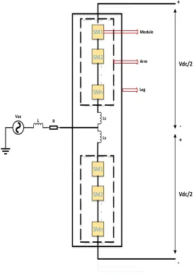
The structure of MMC is made up of two arms, upper and lower, per leg. These two arms are connected through two inductors (Figure 3.1) to control the power flow and protect the system in case a fault condition. Each leg contains N number of series connected SMs. If the number of SMs get higher, the output voltage become smoother and more sinusoidal such that low 𝑑𝑣/𝑑𝑡 can be achieved.
Figure 3-1: Single Phase MMC Structure .
. .
SM1
SM2
SMn
. . .
SM1
SM2
SMn
Module
Arm
Leg
+
-Ls
Ls
-+ Vdc/2
Vdc/2
L R
8
a) b)
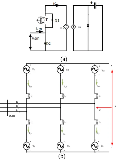
Figure 3-2: Structure of a) half-bridge SM, b) full-bridge SM
Each MMC leg is composed of N number of SMs which result into a line-to-neutral voltage waveform of (N+1) level [14]. SMs can be half-bridge in fig. 3.2 (a) or full-bridge fig. 3.2 (b). Half-bridge SMs are mostly preferred for the applications. The reason for this is that it has lower losses and cost comparing with the full-bridge SMs. Although using a full-bridge SM increases the losses and the cost almost a twice, it also has some important advantages. The most critical of the advantages is providing a counter voltage in case of dc-side short circuits to prevent the fault current flowing from the ac side to the fault on the dc side. Switches in a SM are controllable that is fired in a complementary fashion. Since the half-bridge scheme is adopted throughout this thesis, only its operation principle described. Output voltage of a SM can be equal to its capacitor voltage 𝑉𝑐 or zero depending on the switching states [6].
Table 3-1: Switching States of Half-bridge SMs
State T1 T2 Vsm
On State On Off Vc=Vsm, Ism=Ic
Off State Off On Vsm=0, ,-./
-0 = 𝑖𝑐 = 0
T1 T2 C D1 D2 Vsm Ism + -Vc T1 T2 C D1 D2 Vsm
Ism +
-T3
T3 D3
9 a) b) c) d)
Figure 3-3: Switching States of Half-bridge SMs
For the operation of any SM, it is mandatory that the power flow is balanced over time if the normal operation conditions are desired. Thus, individual capacitor voltages need to be distributed as even as possible. The switching state of semiconductors depends on modulation waveform. If 𝐼𝑠𝑚 > 0 and T1 conducts or 𝐼𝑠𝑚 < 0 and D1 conducts the SM capacitor inserted and its voltage 𝑉𝑐 is shown at the output 𝑉𝑠𝑚 (case a and d). Likewise, if 𝐼𝑠𝑚 > 0 and D2 conducts or 𝐼𝑠𝑚 < 0 and T2 conducts, the SM capacitor is bypassed. Thus, its voltage stays the same. Once the SM capacitor is inserted in the arm, it can be charged or discharged depending upon the direction of the arm current Ism.
3.2.
Modelling and operation of single and three phase MMC
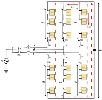
In Figure 3.1 single phase MMC is shown. To extend the single phase to three phases, two more identical phases (b and c) can be added. The system becomes three upper arms, three lower arms total three legs and six arms, as seen in Figure 3.2.
10 Figure 3-4: Three-phase MMC Structure
Parameters in Fig. 3.2 can be defined as following;
• 𝑉𝑎𝑐 is the AC system source voltage
• L and R on the AC side, represent lumped impedance on the line between the MMC and AC grid
• Ls on the MMC, represent inductance of each arm of the converter
• 𝑉𝑢𝑥 and 𝑉𝑙𝑥 stand for the total voltage of the upper and lower arms, respectively and x represents phases a,b and c.
• 𝐼𝑢𝑥 and 𝐼𝑙𝑥 stand for the currents flow through upper and lower arms, respectively and 𝑥 represents phases a, b and c.
• Red dotted lines represent circulating currents in the converter SM1 SM2 SMn + Ls Ls SM1 SM2 SMn SM1 SM2 SMn SM1 SM2 SMn SM1 SM2 SMn SM1 SM2 SMn
-Vua Vub Vuc
Vla Vlb Vlc
Ls Ls Ls Ls + + + + + + -L R AC L R L R C1 Vdc
Iua Iub Iuc
11 In conventional VSC converters, the energy is stored in common link DC bus capacitor, but in an MMC converter, all submodules have their intrinsic capacitors as seen in Figure 3.2 a and b which reduces the cost and increases the reliability. With the help of modulation techniques, it is desired to keep these capacitors voltage distributions as even as possible to get smooth AC voltage waveform. The number of levels at the AC voltage waveform is the number of SM per arm plus one to account for the zero level. If all the SMs are inserted at the same time, the total DC voltage becomes 2𝑉-/. The sum of the individual capacitor voltages in an arm is equal to 𝑉𝑑𝑐.
𝑉-/ = 𝑉/,>,? 𝑋 𝑁BC (3.1)
Where 𝑁BC is the number of SMs per arm and 𝑉/ is the nominal capacitor voltage. If the half of the SMs in the upper arm are inserted and half of the SMs in the lower arm inserted, the instantaneous value of the AC voltage will be zero. The average voltage can be calculated with 𝑒𝑞. (3.2).
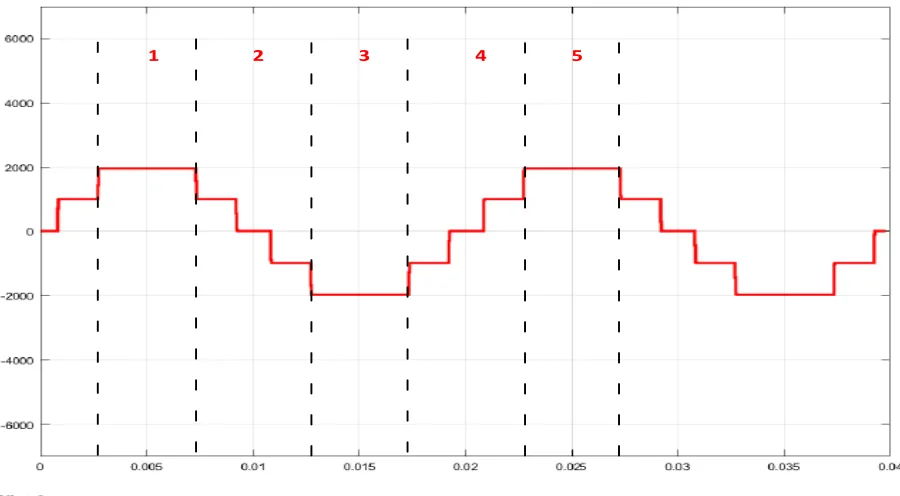
12 Figure 3-5: Five-level MMC Output Voltage Waveform
As can be seen figure above, although there are four SM per leg (N=4), the output will be expected N+1 level. One of the critical design consideration of modulation is that all SMs per leg cannot be operated at the same time. Only half of them are allowed to operate to give the 𝑉𝑑𝑐, otherwise 2𝑉𝑑𝑐 is seen at the output.
In section 1; the MMC gives the maximum output voltage making all the SMs in the upper arm bypassed and keep the capacitor voltages at the same level. On the other hand, all the SMs in the lower are inserted.
In section 2: output voltage seems decreasing gradually inserting some of SMs in the upper arm and bypassing some others in the lower arm. However, the total number of SMs connected per leg must be the same for any instant.
In section 3: this case is the same as section 1, yet this time all the upper SMs are inserted and all the lower ones are bypassed and keep their capacitor voltages remain.
13 In section 4: the output voltage reaches the minimum peak in previous section, now it gradually starts peaking again by inserting some SMs in the lower arm and bypassing some others in the upper arm.
In three phase MMC, there are three types of currents, DC current, AC current and a circulating current. Circulating current term is introduced with MMC topology and it flows through six arms. In normal conditions, DC current is divided by three among legs, AC current is evaluated per leg basis and it is divided two among arms for each phase. Circulating current occurs because of imbalances between SM voltages in each arm, yet it does not have any effect on the output of the MMC. However, it does have an effect on the efficiency, negatively so circulating current suppressing controller will be implemented in next chapters. Upper and lower arm currents mathematically expressed as follows;
𝑖𝑢𝑎 =GHIJ
K +
GMI
N + 𝑖/GO/ (3.3)
𝑖𝑢𝑏 = GHIQ
K +
GMI
N + 𝑖/GO/ (3.4)
𝑖𝑢𝑐 =GHIR
K +
GMI
N + 𝑖/GO/ (3.5)
𝑖𝑙𝑎 = −GHIJ
K +
GMI
N + 𝑖/GO/ (3.6)
𝑖𝑙𝑏 = −GHIQ
K +
GMI
N + 𝑖/GO/ (3.7)
𝑖𝑙𝑐 = −GHIR
K +
GMI
N + 𝑖/GO/ (3.8)
14 𝑖/GO/S =G>STG?SK −UVR
N (3.9)
𝑖/GO/W =G>WTG?WK −UVR
N (3.10)
𝑖/GO// = G>/TG?/K −UVRN (3.11)
𝑖/GO/S+ 𝑖/GO/W+ 𝑖/GO// = 0 (3.12) Arm voltages can be expressed mathematically applying KVL as following;
𝑉>S =.VR
K − 𝑉SX − 𝐿𝑠 -GZJ
-0 (3.13)
𝑉>W =.VR
K − 𝑉WX − 𝐿𝑠 -GZQ
-0 (3.14)
𝑉>/ =.VR
K − 𝑉/X − 𝐿𝑠 -GZR
-0 (3.15)
The dc-link voltage 𝑉-/ can be mathematically expressed as following;
𝑉-/ = 𝑣>S+ 𝑣?S + 2𝐿𝑠-GR[\R
-0 (3.16)
3.3.
Switching and average model of MMC
15
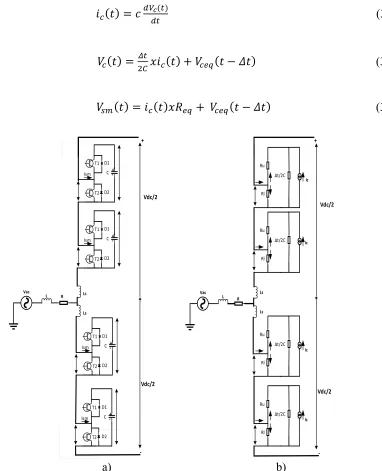
a) b)
Figure 3-6: Structure of a) a half-bridge SM b) structure of Dommel EMT representation of a half-bridge
𝑖/(𝑡) = 𝑐-.-0R(0) (3.17)
𝑉/(𝑡) =K,_0𝑥𝑖/(𝑡) + 𝑉/`a(𝑡 − 𝛥𝑡) (3.18)
𝑉BC(𝑡) = 𝑖/(𝑡)𝑥𝑅`a + 𝑉/`a(𝑡 − 𝛥𝑡) (3.19)
a) b)
Figure 3-7: Structure of a Single Phase MMC a) Half-bridge SM b) Dommel EMT Representations
T1 T2 C D1 D2 Vsm Ism + -Vc Ru Rl Δt/2C Ism Vsm Ium Ilm Vc + -Ls Ls Vdc/2 Vdc/2 L R Vac T1 T2 C D1 D2 Ism +
-T1
T2 C D1
D2 Ism +
-T1
T2 C D1
D2 Ism +
-T1
T2 C D1
D2 Ism +
16 Since the SMs share the same current flows through the arm, total arm voltages can be expressed in eq. 3.21 and 3.22;
𝑉>(𝑡) = ∑ 𝑉>e BC(𝑡) (3.20) 𝑉?(𝑡) = ∑ 𝑉?e BC(𝑡) (3.21)
The operation of the structure in fig 3.6 b, is the same as in fig 3.6 a. depending upon the switching operation, on or off resistance of the controllable switches is mimicked. Dynamic of the SM within each 𝛥𝑡 time step can be mathematically expressed as follows;
f
g?Tg> g>hg?
ij g> ij
g>
_0TK,g? g?_0
k l𝑉𝑠𝑚𝑉𝑐 m = l𝐼𝑠𝑚𝐼𝑐 m (3.22)
In Figure 3.8, a half-bridge SM has built with controllable voltage and current source to reduce the simulation speed for MMCs with the high number of SMs, yet the operation principle is the same.
(a)
(b)
17
Chapter 4
MMC Modulation Techniques
Modulation technics for an MMC can be explained in two different categories, Pulse Width Modulation (PWM) and Nearest Level Modulation (NLM) technics. While PWM requires voltage balancing and averaging control technics for implementation in RTDS, NLM requires Circulating Current Suppressing Control (CCSC).
4.1.
Sinusoidal Pulse-Width Modulation (SPWM)
There are different modulation technics for generating gate signals for controllable switches in this case for IGBTs. Sinusoidal Pulse-Width Modulation and its derivatives are most commonly used. The main idea behind this modulation technic is that a set of triangular carrier waveforms (usually 10 times faster) are generated to compare with a normalized reference sinusoidal waveform. However, it is a tradeoff that the user wants to have lower switching losses with relatively high harmonics or lower harmonics with relatively higher switching losses with higher switching frequency. PWM technic does not change for any cases when the reference is higher than the carrier, a “high” signal is sent to the switch, and otherwise a “low” signal is sent. This can be easily seen in figure 4.4. In the figure below, yellow line represents the normalized sinusoidal waveform, while the red triangular waveform is a carrier signal. As a result of this comparison, green line is produced.
18
4.2.
Phase-Shifted Sinusoidal Pulse-Width Modulation (PS-SPWM)
In this switching technic, many different phase-shifted triangular carrier waveforms are compared with normalized sinusoidal reference waveform [24]. The carriers are phase-shifted to reduce the harmonics at the output signal. To implement this switching technic to a MMC system with higher number of SMs brings a lot of complexities because the number of carrier frequencies should increase proportionally with the modules and the scheme becomes very complex. In figure 4.5, five carrier frequencies and one reference sinusoidal sine wave are shown. The thick yellow line shows the overall number of inserted modules.
Figure 4-2: PS-SPWM Pattern
4.3.
Phase-Disposition Sinusoidal Pulse-Width Modulation
(PD-SPWM)
19
4.4.
Nearest Level Modulation (NLM) Technic
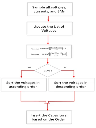
NLM is an alternative method to carrier-based PWM for modulation of MMCs. Although PWM modulation generates better voltage quality than that of NLM. Nevertheless, in case of higher number of SMs required, it is easier to implement the NLM since its computational time less than PWM. Basic idea behind NLM is to determine the number of cells to be inserted or bypassed on the comparison of the modulating signal Vref(t) with the voltage steps that represent idealized cell capacitor voltages [25]. Unlike PWM technic, there is no carrier signal in NLM modulation technic so modulation index and harmonic content in the output can be manipulated by changing the sampling frequency. Again, losses and harmonics tradeoff take in place while deciding the sampling frequency. To determine the minimum required sampling frequency eq. (4.1) can be used. In this case, 𝑓B can be regarded as the limit for harmonic content, if 𝑓B increases more, harmonics cannot go further.
𝑓B = 𝑓𝜋𝑁BC (4.1) To calculate the number of SM inserted in the upper arm;
𝑛GqB`O0`- = 𝑟𝑜𝑢𝑛𝑑 lt
u.v.VRi.\wxJ,Q,R
.R ym (4.2)
Where N=Total number of SM in an arm, 𝑛Wz{SBB`- = 𝑁 − 𝑛GqB`O0`-.
To calculate the number of SM inserted in the lower arm; 𝑛GqB`O0`- = 𝑟𝑜𝑢𝑛𝑑 lt
u.v.VRT.\wxJ,Q,R
.R ym (4.3)
Where N=Total number of SM in an arm, 𝑛Wz{SBB`- = 𝑁 − 𝑛GqB`O0`-.
20 charging. There also previously bypassed capacitor with high voltages exist. To discharge these capacitor, they need to be inserted when the arm current is negative such that they can start discharging. There are also previously inserted SM capacitors need to be bypassed to balance their voltages. Capacitors with the highest voltages are chosen if the arm current is positive so that they stop charging and capacitors with the lowest voltages are chosen if the arm current is negative such that they stop discharging. Fig. 4.3 shows the NLM algorithm flowchart.
Figure 4-3: NLM Algorithm
Sample all voltages, currents, and SMs
iarm>0 ?
Yes No
Sort the voltages in
ascending order Sort the voltages in descending order
Update the List of Voltages
21
Chapter 5
Power Flow and MMC Control
5.1.
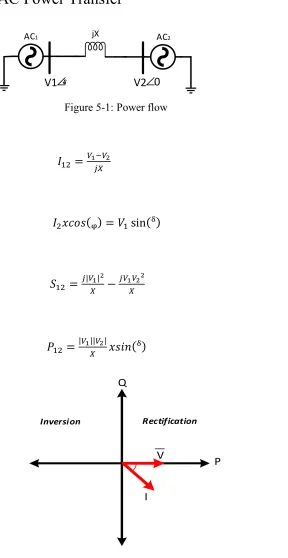
Principle of AC Power Transfer
Figure 5-1: Power flow
𝐼jK =.|i.}
~• (5.1)
𝐼K𝑥𝑐𝑜𝑠(ᵩ) = 𝑉jsin(ᵟ) (5.2)
𝑆jK =~|.||}
• −
~.|.}}
• (5.3)
𝑃jK = |.|•||.}|𝑥𝑠𝑖𝑛(ᵟ) (5.4)
Figure 5-2: Power Transfer Scheme
AC1 AC2
GND2 GND3
jX
V1 V2 0
P Q
V
I
22 If the arm voltage and the arm current is positive, power flows from DC bus to AC grid which is an inversion operation. Likewise, both current and voltage are negative, power flows the same direction. Unlike, if the arm current is positive, and the arm voltage is negative to the reference point, power flows from AC grid to DC bus, which is a rectification operation. Similarly, if the arm current is negative and the arm voltage is positive to the reference point, this is a rectification operation.
5.2.
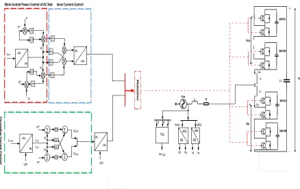
Control of MMC
Control system of an MMC for HVDC system can be complex because of high number of SMs and their control structure, shown in fig. 5.3. As mentioned before, the energy is not stored one bulk DC link capacitor, instead the energy needs to be stored as evenly as possible among the SM capacitors with the help of the specific control algorithm. A vector control technic, calculating a voltage-time area across the converter equivalent inductor ˆ‰
K, which is used for changing the
current from the present value to the reference value, is used in the MMC converters. The 𝑑𝑞 reference frame current orders to the controller are calculated from preset P and Q powers, and preset 𝑉𝑎𝑐 and 𝑉𝑑𝑐 voltages. Controller of AC voltage, producing the modulated switching pattern, is controlled by the inner controller. To control the active and the reactive power independently proportional-integral (PI) controller are used [20], [21]. The control system in 𝑑𝑞 frame is used as the d axis current control for active power control whereas q axis current control for reactive power control. To control the active power, frequency or DC voltage can be controlled or a power reference can be set. Reactive power can be controlled by AC voltage control or reactive power reference can be set. 𝑉Ga is forced to zero by PLL and it will yield eq. 5.5 and 5.6
𝑃G+ 𝑗𝑄G = NKŒ𝑉G- + 𝑗𝑉Ga•Œ𝑖-+ 𝑖a• , 𝑃 =NK𝑉-𝑖- (5.5) 𝑄 = −N
23
Figure 5-3: Control Scheme of Single Phase MMC
5.3.
Mathematical Expressions of the operation of MMC Converters
In order to build a controller, both AC and DC sides need to be modelled mathematically [4]. Figure 3.4 is taken as a reference for the following calculations;
AC side dynamics are expressed as following where 𝑖S, 𝑖W , 𝑖/ are the leg currents while 𝑣S, 𝑣W, 𝑣/ are AC side voltages where .ZŽi.•Ž
ˆ = 𝑢h, x=(a,b,c). -GJ(0)
-0 =
.J
ˆ − 𝑢h (5.7) -GQ(0)
-0 =
.Q
ˆ − 𝑢h (5.8) -GR(0)
-0 =
.R
ˆ − 𝑢h (5.9)
If 𝑑𝑞 park transformation is applied to equations 5.7 through 5.9;
+ Ls Ls -Vua Vla + + -C1 Vdc Iua Ila L R Vac abc dq abc dq Vabc iabc
Vd Vq id iq A B C
PLL Phi (ᵩ) SM #1 SM #N SM #1 SM #N T1 T2 C T1 T2 C T1 T2 C T1 T2 C Ci rc u la tin g Cu rr e n t Co n tr o l iabc dq abc Id Iq PI 2/3 -+ P P* ++ --++ + -Q Q* 2/3 PI WL WL PI PI + -dq abc Main Control Power Control of AC Side Inner Current Control
24 𝐿-GV
-0 = 𝑉- − 𝑢- + 𝐿𝑤𝑖a (5.10)
𝐿-G‘
-0 = 𝑉a− 𝑢a− 𝐿𝑤𝑖- (5.11)
w in eq. (5.10 and 5.11) is the angular frequency of the system. In normal conditions, 𝑉a in eq.
(5.11) is zero.
P in eq. (5.5) is the real power, transferred from AC side to the converter while Q in eq. (5.6) is a reactive power, transferred from AC side to the converter. Voltage across the transformer is generally controls the active power (P). PI controllers are used to compare active power measurement in the system with the reference desired Preference. If Preference >P error signal (e) will be positive and the voltage across the transformer increases. If P>Preference, e will be the negative and the voltage across the transformer decreases. Reactive power (Q) is flows from higher magnitude side to the lower magnitude side and it depends on the magnitude difference in the voltage. Like real power control, PI controllers are also used for reactive control. If Qreference>Q 𝑒 will be positive and modulation index m increases. If Q>Qreference, m decreases.
𝑚- = .V
e.VR and 𝑚a =
.‘
e.VR (5.12)
𝑚 =.X?0S’` S/OXBB ?X“ BG-` X” hCO”.-//K (5.13)
25
5.4.
Capacitor Voltage Balancing Algorithm
Capacitor voltage balancing control is one of the critical part of control systems of MMCs. As the working principle of MMCs, SM capacitors may be charged or discharged depending upon the direction of the arm current. When the 𝐼BC is positive, the capacitor is charged or when the 𝐼BC is negative, the capacitor is discharged. To be able to equate the sum of the individual turned
on capacitor voltages to the DC link voltage, and to distribute the voltages as evenly as possible, a control algorithm is needed. There is sorting and selecting technic to decide the minimum and maximum values among the SM capacitors. The main idea behind sorting algorithm is that if the arm current Ism is positive, the SM, with the lowest voltage in the arm, will turned on and if the arm current Ism is negative, the SM, with the highest voltage in the arm, turned on [6]. In other words, if the capacitor voltages of the SM in the arm higher than the reference voltage, a positive arm power should be taken from the SMs to the DC bus.
Figure 5-4: Capacitor Voltage Balancing Algorithm
Measure and sort all
the capacitor voltages
in each arm
Calculate the number of
SMs to switch on
Non
iarm>0 ?
Yes No
Switched on the Non
SMs with the lowest
capacitor voltages
26
5.5.
Circulating Current Suppressing Controller (CCSC)
Circulating current elimination or minimization is the second important part of the control system after capacitor voltage balancing control. Circulating current exists in an MMC because of the voltage and the phase difference between the upper and lower arms. Circulating current has the second-harmonic component as can be seen in fig. 5.5. Its frequency is double the fundamental frequency and it is phases A, C and B sequence. Although it does not have any effect on the AC side and does not leave the converter, the existence of the second harmonic distorts the arm currents and causes the ripple increment in individual capacitor voltages. As a result, circulating current affects the rating of components, efficiency and losses negatively. There are some ways to suppress the circulating current.
• Increasing the size of the arm inductor which decreases the rapidness of control response and increases the system cost [27].
• Adding a parallel capacitor (resonant filter) in the middle point of a leg [19].
• Implementing the Circulating Current Suppression Control (CCSC) proposed in [28]. As claimed in [19], the CCSC eliminates the second harmonic of AC component of the circulating current and decreases the voltage ripple from 30% to 8%.
Figure 5-5: Circulating Current Equivalent
-2Lo + Vdc Va c_ up pe r Vd c_ up per Va c_ up pe r Vd c_ up per Va c_ up pe r Vd c_ up pe r + + +
2Lo 2Lo
+ + +
- -
27 •
𝑉/GO/S 𝑉/GO/W
𝑉/GO//– = 𝑅 • 𝐼/GO/S 𝐼/GO/W 𝐼/GO//– + 𝐿 •
𝐼/GO/S 𝐼/GO/W
𝐼/GO//– (5.15)
𝑖-G””,S =UVRN + 𝐼K”sin (2𝑤𝑡 + ᵩ) (5.16)
—𝑉𝑉
/GO/-/GO/a˜ = 𝑅 —
𝐼
/GO/i-𝐼/GO/ia˜ + 𝐿 —𝐼𝐼/GO/i-/GO/ia˜+l 02𝑤𝐿 −2𝑤𝐿0 m —𝐼𝐼/GO/i-/GO/ia˜ (5.17) To create control block diagram of CCSC eq. (5.15-5.17) are used. Eq. 5.16 is derived only for Phase A.
28
Chapter 6
Study Systems and Implementations
This chapter is divided in two sections. Proposed feed-forward current control scheme is implemented for MMC based Point to Point HVDC system under balanced and unbalanced grid conditions and results are demonstrated in RTDS in chapters 6.1 through 6.3. In chapter 6.4, ongoing five level back-to-back MMC implementation is presented, and simulated in EMTD/PSCAD and MATLAB/Simulink.
6.1.
Feed-forward Current Control Strategy
The inner current control is a fundamental part of MMC control system. The current control allows other controls such as DC voltage, AC voltage, active power and reactive power controls. The common method to develop the current control is by modelling the AC system of the converter and applying 𝑑𝑞 transformation to represent the three-phase AC system in the synchronous reference frame. This control scheme is implemented for MMC based Point to Point HVDC system which is seen fig. 6.1 and its parameters are seen in tab. 6.1. The Bergeron transmission line model is chosen because time step is (Δt) 50 usec and it does not produce an artificial resonance at high frequencies. 400/333-kV three phase transformer with its secondary winding connected in delta to block the zero-sequence voltages generated by the MMC.
Figure 6-1: Point to Point MMC based HVDC System
29 𝑉B,SW/ = ™
𝑣B,S 𝑣B,W
𝑣B,/š = › 𝑣S
œ sin(𝜃S)
𝑣œ sin(W 𝜃W)
𝑣œ sin(/ 𝜃/)
ž (6.1)
𝑖SW/ = ™ 𝑖S 𝑖W 𝑖/š = ›
𝐼Ÿ sin(S 𝜃S+𝛼)
𝐼Ÿ sin(W 𝜃W+𝛼)
𝐼/
¡ sin(𝜃/+𝛼)
ž (6.2)
𝜃SW/ = ™
𝜃S 𝜃W 𝜃/
š = ¢ 𝜔𝑡 𝜔𝑡 −K¤N 𝜔𝑡 +K¤N
¥ (6.3)
Table 6-1: MMC Based HVDC System Parameters of Figure 6.1
Symbol Description Value Unit
𝑃 Base MVA 1000 MVA
VDC DC voltage 640 kV
𝑣B,SW/ Line-Line AC voltage 400 kV
T Transformer (Yg - Δ) 400/333 kV
N Number of SM per arm 400 -
Vc Capacitor Voltage 1.6 kV
F Fundamental frequency 60 Hz
Lo Arm inductance 45 (15%) mH (PU)
L Transformer inductance 53 (18%) mH (PU)
C SM capacitance 10 mF
Where 𝑣œ, 𝑣S œ,and 𝑣W ¦/ are the peak values of the three-phase AC voltages, and 𝐼ŸS, 𝐼ŸW, and 𝐼Ÿ/ are the peak values of the three-phase AC currents. 𝛼 is the phase-shift between the voltage and the current, and 𝜔 is the fundamental angular frequency. The dynamic equation of AC aside of MMC can be derived by applying Kerchief Voltage Law (KVL) as follows;
30 Where 𝑣C,SW/ the AC output voltages of MMC, and L and R is represent the transformer inductance and the resistance.
Assuming the 𝑑 axis is in phase with the AC voltage 𝑣BS and the 𝑑𝑞 transformation matrix T of the AC voltages and currents is as follows;
𝑇 =K
N ¨
sin(𝜃S)
cos(𝜃S)
sin(𝜃W)
cos(𝜃W)
sin(𝜃/)
cos(𝜃/)« (6.5)
t𝑥𝑥
-ay = 𝑇 ™
𝑥S
𝑥W
𝑥/
š , 𝑥 = 𝑣B,G (6.6)
The dynamic equation of AC side system of MMC is defined in the 𝑑𝑞 reference as follows; 𝑣C,- = 𝑣B,-− 𝑤𝐿𝑖a+ 𝐿-GV
-0 + 𝑅𝑖- (6.7)
𝑣C,a = 𝑣B,a− 𝑤𝐿𝑖-+ 𝐿-G‘
-0 + 𝑅𝑖a (6.8)
𝑖- = jNlcos(𝛼) (𝐼CS+ 𝐼CW + 𝐼C/) − ¬𝐼CScos(2𝑤𝑡 + 𝛼) + 𝐼CWcos t2𝑤𝑡 −K¤N + 𝛼y +
𝐼C/cos t2𝑤𝑡 +K¤N + 𝛼y-m (6.9)
𝑖a =jNlsin(𝛼) (𝐼CS+ 𝐼CW + 𝐼C/) + {𝐼CSsin(2𝑤𝑡 + 𝛼) + 𝐼CWsin t2𝑤𝑡 −K¤N + 𝛼y +
𝐼C/sin t2𝑤𝑡 +K¤N + 𝛼y}m (6.10)
The inner current control is developed to generate the command output voltage of the MMC. However, the 𝑑𝑞 currents and voltages can be decomposed into DC and AC components
𝑖-,-/ 𝑖-,S/
31 in eq (6.9) and (6.10). The AC components cause the double line frequency on the DC voltage, active and reactive power [4], [5]. Thus, the 𝑑𝑞 transformation matric of the voltages 𝑇°Band
currents 𝑇G grid can be written in terms of the AC and DC components as follows;
𝑇°B =j
N¢
1 1 1
−𝑐𝑜𝑠(2𝜃S) −𝑐𝑜𝑠(2𝜃W) −𝑐𝑜𝑠(2𝜃/)
0 0 0
𝑠𝑖𝑛(2𝜃S) 𝑠𝑖𝑛(2𝜃W) 𝑠𝑖𝑛(2𝜃/)
¥ (6.11)
⎝ ⎜ ⎛
𝑣B,--/
𝑣B,-S/
𝑣B,a-/
𝑣B,aS/
⎠ ⎟ ⎞
= 𝑇°B ›
𝑣¸S
𝑣¸W 𝑣¸/
ž (6.12)
𝑇G = jN¢
𝑐𝑜𝑠(𝛼) 𝑐𝑜𝑠(𝛼) 𝑐𝑜𝑠(𝛼)
-𝑐𝑜𝑠(2𝜃S+ 𝛼) -𝑐𝑜𝑠(2𝜃W+ 𝛼) -𝑐𝑜𝑠(2𝜃/+ 𝛼)
𝑠𝑖𝑛(𝛼) 𝑠𝑖𝑛(𝛼) 𝑠𝑖𝑛(𝛼)
𝑠𝑖𝑛(2𝜃S+ 𝛼) 𝑠𝑖𝑛(2𝜃W+ 𝛼) 𝑠𝑖𝑛(2𝜃/+ 𝛼)
¥ (6.13)
⎝ ⎛ 𝑖-,-/ 𝑖-,S/ 𝑖a,-/ 𝑖a,S/⎠
⎞ = 𝑇G › 𝐼ºS 𝐼ºW
𝐼º/
ž (6.14)
Substituting (6.13 and 6.14) into (6.7 and 6.8), 𝑑𝑖𝑑/𝑑𝑡 and 𝑑𝑖𝑞/𝑑𝑡 are derived in terms of AC and DC components, where 𝑖-a = 𝑖-a,-/+ 𝑖-a,S/. Therefore, the AC system dynamic equations of
MMC becomes;
𝑣C,- = 𝑣B,-− 𝑤𝐿Œ𝑖a,-/− 𝑖a,S/• − 𝑒 (6.15)
32 The DC component of 𝑑𝑞 currents 𝑖-a,-/ is used to control the DC components of the DC voltage, active power, reactive power, and AC grid voltages. The proposed feedforward current control is developed based on equations (6.15) and (6.16) and visualized in fig. 6.2.
(a)
(b)
(c)
33
6.2.
Real Time Simulation of Proposed Model in Real Time Digital
Simulator (RTDS)
To be able to simulate the system in real time [29], RTDS hardware, which its cubical, called a rack and accompanying software, RSCAD, are used. A rack connects to various cards for different applications in real time. In fig.6.3, the system implementation is shown. To implement the system, FPGA based MMC support unit and RTDS are used.
(c)
Figure 6-3: HIL Implementation of the System
There are certain rules regarding implementation a system in RSCAD. The user needs to be aware of the capacity of the rack and physical connections, as well. In the case of MMC implementations, if the number of SMs per arm is high and the switching model, explained in chapter 3.3, is used, MMC support units, will be explained later, will be used. However, if the number of level is not too many, PB5 cards generally enough to model the system. There are also other cards, which are I/O GTDO, and GTAI, along with the rack. GTDO card is a digital output
FPGA - 2
FPGA - 1
FPGA - 3
FPGA Based MMC Support Unit RTDS Rack
34 card, providing up to 64 output signals. Output signals are needed to be determined in RSCAD while the system was being build.
Figure 6-4: GTAO, GTDO and GTAI Cards
35 GTAI Card: The Gigabit Transceiver Analogue Input Card is for interfacing analogue signals from an external devices to the RTDS. This card includes twelve analogue input channels with each channel configure as a differential input range +−10 V [24]. GTAI cards can take the voltages of MMC storage devices as long as its rated voltage in the range.
GTDO Card: The Gigabit Transceiver Digital Input Card (GTDO) is for interfacing digital signals from the RTDS to external devices. The cards includes 64 optically isolated digital output channels [24].
36 Figure 6-5: Interface Transformer between Small-time Step and Large-time Step
In this system, rtds_vsc_MMC_FPGA_U5 model, seen in figure 6.5, is used to simulate legs as a block. Calculations are made in FPGA and interfaced into the PB5 processor card, which is located in the rack, with a Bergeron ½ small time-step travel-time interface t-line [24]. Each SM needs 8-bit firing pulse input word. If there are maximum eight SM, they can be packed into two 32-bit integers and sent to the FPGA from the PB5. If there are more than eight SMs, extra physical connection needs to make to a controller.
37 The RTDS and FPGA based MMC support unit investigate the dynamic and quality performance of the proposed feedforward current control strategy. FPGAs are able to make calculations up to 512 SMs. Even if the user is modelled the system based on 400 SM per leg, like in this case and can be seen in figure 6.5, FPGAs still make the calculations for 512 SMs. The results from the superfluous 112 SMs are thrown away, but the calculations are still done. The MMC system controls the active and reactive power while the DC voltage is regulated using a controllable DC supply. Regarding the working principle of MMC models in RSCAD;
Ø At the beginning, all the SMs are blocked with no gate signal applied
Ø Intrinsic capacitors are charged through the anti-parallel diodes
Ø Once they are evenly charged and the terminal voltage is stabilized, the SMs are de-blocked
Ø Then, the control scheme comes into the picture like in figure 6.6
38 Figure 6-8: Phase Lock Loop (PLL) and Park Transformation Implementation in RSCAD
The function of the PLL is to synchronize the firing pulses of the firing generator with AC system. The gain and time constant of PLL should be selected to track the changes in AC system frequency while still providing acceptable firing accuracy. Gain of PLL is made as large as possible to provide greater stability so in this MMC configuration PLL gain is 50. The PLL is a second order system, if it is given high loop gain like in this particular case, it tends to follow AC system phase with small transient error. When the PLL block is locked, the output PHI=The2 represents the phase 2𝜋 < 𝑃𝐻𝐼 < 0 of phase A input (N12pu) [24].
Three phase to DQ0 transformation is that DQ0 blocks convert a three phase rotating vector set to a stationary vector set using Park transformation [24].If The2 is fixed at 0 and inputs N12, N22 and N32 which are the bus voltages are a balanced set of positive sequence signals, the output d in figure 6.7 leads q by 90 degrees. Thus, q will be in phase with phase A voltage eq. (6.15). If q leads d by 90 degrees, then d will be in phase with phase A voltage eq. (6.16).
•𝑑𝑞 0
– =K
N∗ f
sin(𝑇ℎ𝑒2) cos(𝑇ℎ𝑒2)
j K
sin(𝑇ℎ𝑒2 − 120) cos (𝑇ℎ𝑒2 − 120)
j K
sin(𝑇ℎ𝑒2 + 120) cos(𝑇ℎ𝑒2 + 120)
j K
k •𝑉𝑎𝑉𝑏 𝑉𝑐
39 •𝑑𝑞
0 – =K
N∗ f
cos(𝑇ℎ𝑒2) sin(𝑇ℎ𝑒2)
j K
cos(𝑇ℎ𝑒2 − 120) sin (𝑇ℎ𝑒2 − 120)
j K
cos(𝑇ℎ𝑒2 + 120) sin(𝑇ℎ𝑒2 + 120)
j K
k •𝑉𝑎𝑉𝑏 𝑉𝑐
– (6.16)
An FPGA based MMC support units, shown in figure 6.8, contain a Xilinx Virtex FPGA board (VC707) and two 8 fiber communication daughter boards from Faster Technologies (FM-S18). Additionally, there are 16 more fiber port for extra model. One VC707 FPGA board has an ability to support up to six MMC phase arms, but there are two more FPGAs are needed for the firing control for the upper and lower arms of A, B and C phases.
40
6.3.
Simulation Results of Point to Point MMC Based HVDC System
41 Case #1: Dynamic performance of t is analyzed with the feedforward controller. It can be seen in fig. 6-10 (a), the three phase grid currents, in (b) the three phase grid voltages and in (c), (d) upper and lower capacitor voltages of MMC1 and MMC2, respectively seem as expected with the feedforward current controller. Both controllers keep the DC link voltage at 1 PU.
(a)
(c)
(e)
(b)
(d)
(f)
42 Case #2: Power reversal is tested by changing the power reference at t=0.15s from -500 MW to 500 MW using a 200 𝑚𝑠 ramp reference. Figures show that the system can suddenly reverse the power flow direction by reversing the power set point at MMC-1. Reactive power reference remains unchanged. It reacts because of the dynamic, but it gets back to the reference value in 200ms.
(c)
43 Case #3: In this case, the differences between conventional and proposed controller is shown in case of balanced and unbalanced grid conditions. Power in fig. 6-12 does not track the reference as good as in fig 6-11 so the steady state error is smaller with the proposed controller. In fig. 6-12, grid currents are not quite zero at the zero crossing unlike in fig. 6-11. Although circulating current does not effect on the AC side it still has an effect on efficiency. SLG fault is applied for a second on the high voltage (HV) side of the 400/333 kV transformer of MMC-1 in fig. 6-12 with and without the proposed controller are seen, respectively. During the fault, DC overvoltage is limited to 10% by the DC voltage controller in 6-12.
44 Case #4: Circulating current is analyzed when a SLG fault occurs at t=0.5s.
without proposed controller with proposed controller
(a)
(c)
(b)
(d)
(e) (f)
45 The double-fundamental frequency component is added to circulating currents. Thus, the second harmonic content is expected to be higher. Fig. 6-13 shows FFT analysis of the circulating current under SLG fault phase a, b, and c, respectively. As can be seen in fig. 6-13 (d-f), the proposed current controller helps to reduce the second harmonic content as compared to the second harmonic content results with the conventional current controller in fig. 6-13 (a-c).
Case #5: Grid current is analyzed when a SLG fault occurs at t=0.5s. Results show that the proposed current controller scheme reduces Total Harmonic Distortion (THD) in grid current. Fig. 6.14 (a) shows the dynamic performance of the three-phase grid current under SLG fault without and fig. 6.14 (b) with the proposed current control scheme. Table 6-2 shows the how the proposed current control scheme improves the THD on the secondary (Δ). Based on IEEE STD 519, 50 harmonic components are considered to calculate the THDs of the grid currents.
(a)
(b)
46 Table 6-2: Total Harmonic Distortion of the Grid Currents under SLG Fault
THD% Without
feedforward Current Control
Scheme
With feedforward Current Control
Scheme Phase-a (Faulty
Line) 1.41% 1.1%
Phase-b 1.35% 0.45%
Phase-c 1.55% 1.36%
47 Both Converters Operate Both Converters are Blocked
Figure 6-15: System Dynamics under DC Fault with Half Bridge SM Topology
Both Converters Operate Both Converters are Blocked
48 VSC behaves as harmonic load from grid point of view if a proper control scheme is not employed. Filters cannot eliminate harmonics since the MMC is designed for high frequency. Implementing the feed-forward current control scheme allows;
• Not to concern about bandwidth and stability due to its open loop characteristics
• Less dependence on PI controllers while improvement on system dynamic
• To suppress the second harmonic in the circulating current
• No negative effect on main control objects of the system
• To decrease THD in the grid currents of the converter
49
6.4.
Five Level Back to Back MMC Hardware Implementation
In this chapter, ongoing back to back MMC implementation is discussed. Hardware implementation is a collaborative work with Mr. Mohammed Alharbi who is a Ph.D. student at NC State university under Dr. Subhashish Bhattacharya. The main purpose of this implementation is to transfer energy between converters. While MMC –I controls the DC voltage, MMC- II controls the active power as seen in fig 7.6.
𝑉-/ = 𝑁BC𝑥𝑉/ = 2𝑥𝑉/ = 300𝑉 => 𝑉/ = 150𝑉 (6.17) The SM capacitance 𝐶 = KÁÂÂRB
ÃFJ\Â.R} where EÅÅÆ= 0.5𝐶BC𝑣-/
K (6.18)
Where S is the nominal capacity of the MMC, EÅÅÆis the energy per megavolt-ampere (MVA). NÈÉÅ is the number of SM per arm.
The capacitor rating is usually designed considering the amount of energy that the capacitor can store. The capacitor time constant is often used as a measure of the amount of capacitor energy which is defined as follows;
𝜏 =,h`|\}
KhË|\ = 24ms (6.19)
It is claimed that the total energy stored per rated power is typically 30-40kJ/MVA, which leads to a capacitor time constant of 40ms. In this thesis, 24ms is assumed.
To calculate the arm inductor, some approximations have to be done as follows;
𝑤u = 314𝑟𝑎𝑑/𝑠 𝑖𝑛 𝑐𝑎𝑠𝑒 𝐿X < 0.2𝑝𝑢 This assumption mostly valid for VSC based HVDC project [25]
.VRh.}x
Îh“Ï}hˆÏ > 10
UVRh.}x
Ãh“Ï ≫
UVRh.}x
50 When calculating the arm inductor, double fundamental frequency AC component because of circulating current, explained in chapter 5.5, needs to be considered. Thus, capacitor voltage of an individual SM;
𝑉/(𝑡) = 𝑉/ +.}x
KF𝑥𝑠𝑖𝑛(2𝑤X𝑡 + 𝛼) (6.21)
Then, double fundamental frequency becomes; 𝑈K” =Ãh“Ë
Ï/(𝐶𝑥𝑉/ −
.VR
Îh“Ï}hˆÏ) (6.22)
Since the peak value of the circulating current at double fundamental frequency, explained in chapter 5.5, it is easy to calculate the first design criteria of the inductor.
𝐿SOC= ( Ë
NhU}x+ 𝑉-/𝑥
j
,h.RhΓÏ}) (6.23)
One of the reasons why the arm inductor is used because of limiting the fast current rise in abnormal situations.
𝑉-/ = 𝐿SOC-GZ
-0 + 𝐿SOC -G•
-0 (6.24)
To calculate the second criteria of the arm inductor, fault current rise 𝛼 needs to be expressed mathematically [25].
𝛼 =-GZ
-0 =
-G•
-0 =
.VR
KˆJ\Â (6.25)
𝐿SOC= .VR
KÒ (6.26)
51 Table 6-3: List of Parameters
Rated Power (W) 2000
Rated L-L Voltage (V) and 𝑉{`Se (𝑉) 160
𝑉ˆˆ =
138𝑘𝑉
√3 𝑥√2 = 130.6
Modulation
𝑚 =.X?0S’` S0 0×` ˆX“ ØG-` .-//K = jÃu h
√} √Ù
jvu = 0.87
DC Voltage (V) 300
Rated Current (A) 𝐼 = 𝑃
√3𝑥𝑉ˆˆ
= 7.21
Rated Frequency (Hz) 60
Number of SMs per Arm (N) 2
DC Capacitor Voltage (V) 150
Carrier Frequency (Hz) 2000
Arm Inductance 𝐿SOC (mH) 1
54 Table 6-4: Analog Measured Parameters
Analog Inputs from the Hardware Implementation Calculated Parameters
Grid Voltages
𝑉𝑎𝑏 𝑉𝑏𝑐 𝑉𝑐𝑎=𝑉𝑏𝑐+𝑉𝑎𝑏
Grid Currents
𝐼𝑎 𝐼𝑏 𝐼𝑐=𝐼𝑎+𝐼𝑏
Capacitor Voltages
𝑃ℎ𝑎𝑠𝑒 𝐴 𝑣Sj 𝑣SK 𝑣SN 𝑣SÜ
𝑃ℎ𝑎𝑠𝑒 𝐵 𝑣Wj 𝑣WK 𝑣WN 𝑣WÜ
𝑃ℎ𝑎𝑠𝑒 𝐶 𝑣/j 𝑣/K 𝑣/N 𝑣/Ü
DC Voltage
𝑉𝑑𝑐
Circulating Currents
𝑃ℎ𝑎𝑠𝑒 𝐴 𝑖/GO/iS 𝐼>S = 0.5𝑥(𝑖/GO/iS+ 𝐼S)
𝑃ℎ𝑎𝑠𝑒 𝐵 𝑖/GO/iW 𝐼?S = 0.5𝑥(𝑖/GO/iS− 𝐼S)
𝑃ℎ𝑎𝑠𝑒 𝐶 𝑖/GO/i/ 𝑇ℎ𝑒 𝑐𝑎𝑙𝑐𝑢𝑙𝑎𝑡𝑖𝑜𝑛𝑠 𝑓𝑜𝑟 𝑝ℎ𝑎𝑠𝑒 𝐵 𝑎𝑛𝑑 𝐶
6.4.1.
Control System of the Hardware
The main controller of the system is the fault-tolerant controller for MMCs [29] with the following features;
Ø Network controlled architecture in which slave controllers are managed by the master controller.
Ø Failure in slave controller can be bypassed by adjacent slave controller.
Ø To avoid single point of failure, master controller and communication link must be redundant.
55
Ø The board is seen Fig 6.23 has 13 DSP controller boards, which are distributed as 3 slave phases (four controllers for each phase) and 1 master controller
Ø The board has 3 FPGA controllers, used for fault detection and routing between different controllers. All the routing takes between the controllers takes place via FPGAs.
Ø None of the controller is connected to the other directly.
56 Figure 6-20: Fault Tolerant Controller Main Board
6.4.2.
Main Control of the System
PLL is generated as mathematically explained in the previous chapters.
𝑇ℎ𝑒𝑡𝑎_𝑏 = 𝑇ℎ𝑒𝑡𝑎_𝑎 − K¤N
57 Three phase voltages and currents are transformed into 𝑑𝑞 reference frame.
Figure 6-21: General Overview of Control Algorithm
Outer control block diagrams;
Figure 6-22: Outer Control Block Diagrams
abc/dq
Va
Vb
Vc
Vd
Vq
abc/dq
Ia
Ic
Ib
Id
Iq
Theta_a Theta_a
Outer loop
Control Control loopCurrent
CCSC
+ - Nearest Level
Modulation
Capacitor Balancing Control
Gate Signals P*
Q*
I* Vc*
Vdiff* Icirc*=0
58 Inner Current Control (ICC) block diagram;
Figure 6-23: ICC Block Diagram
𝑉-O`”∗ß.
V− 𝑤𝐿 ∗ 𝑖a+ 𝑃𝐼𝑥(𝐼-O`”− 𝐼-) (6.27)
𝑉aO`”∗ß.
‘ + 𝑤𝐿 ∗ 𝑖-+ 𝑃𝐼𝑥(𝐼-O`”− 𝐼-) (6.28)
𝑃𝐼 = 𝐾{+á[
B (6.29)
Getting the output response from the inner current control block diagram, then transform them to abc reference frame;
Idref*
-+
Id
PI ++-
Vdref*
-+
I
qI
qref* PI +++
Vqref*
59 Figure 6-24: DQ0 to ABC Conversion Block Diagram
One of the most important step in the control algorithm is to control of individual SMs. To do this, averaging and balancing control methods are used [26]. The fig. 6.29 shows the circulating and averaging control for only phase A, but it is the same for phases B and C. The averaging control is used to force the average capacitor voltage of all SMs per leg to follow the reference value 𝑉/,Ṡ
Figure 6-25: Circulating and Averaging Control for Phase A
𝑉h =.R|JT.R}J
K (6.30)
dq/abc
Vqref
Vdref
Varef
Vbref
Theta_a
Vcref
K5
Vx
Vy
-+
+
+
Sin(theta_a)
+ -PI
-+
Vdc*0.5
Vk
K5
Vavg_a
0.5
60 𝑉z = .RÙJT.RãJ
K (6.31)
𝑉e =.R|JT.R}JT.Ü RÙJT.RãJ (6.32)
Figure 6-26: Block Diagrams for Capacitor Balancing Algorithm for Phase A
Voltage command to each SM, can be calculated as follows for phase A. 𝑉O`”Sj = .VR
Ü + 𝑉S°’_S+ 𝑉WS?j−
𝑉SO`” 2
ä (6.33)
𝑉O`”SK = .VR
Ü + 𝑉S°’_S+ 𝑉WS?K−
𝑉SO`”
2
ä (6.34)
𝑉O`”SN = .VR
Ü + 𝑉S°’_S+ 𝑉WS?N+
𝑉SO`” 2
ä (6.35)
𝑉O`”SÜ = .VR
Ü + 𝑉S°’_S+ 𝑉WS?Ü+
𝑉SO`” 2
61
6.4.3.
Simulation Results of Five Level MMC Converter
The system was tested in PSCAD/EMTC and MATLAB/Simulink.
63
Chapter 7
Conclusion
Feed-forward current control is a powerful method to reduce the unwanted disturbances in a control system. It is also more efficient in time-varying systems for tracking. In this thesis, feedforward current control method is presented and investigated for Point to Point MMC based HVDC system under normal and abnormal operation conditions. VSC behaves as harmonic load from grid point of view if improper control scheme is not employed and filters cannot eliminate harmonics since the MMC is designed for high frequency.
Implementing the feed-forward current control scheme allows;
• Not to concern about bandwidth and stability due to its open loop characteristics
• Less dependence on PI controllers while improvement on system dynamic
• To suppress the second harmonic in the circulating current
• No negative effect on main control objects of the system
• To decrease THD in the grid currents of the converter
64
List of References
[1] Kazmierkowski, M. P., & Malesani, L. (1998). Current Control Techniques for Three-Phase Voltage-Source PWM Converters: A Survey. IEEE Transactions on Industrial
Electronics, 45(5), 691–703
[2] Rohner, S., Hiller, M., & Sommer, R. (2010). Modulation, Losses, and Semiconductor Requirements of Modular Multilevel Converters. IEEE Transactions on Industrial Electronics, 57(8), 2633–2642
[3] Flourentzou, N., Agelidis, V. G., & Demetriades, G. D. (2009). VSC-Based HVDC Power Transmission Systems: An Overview. IEEE Transactions on Power Electronics, 24(3), 592– 602.
[4] Guan, M., & Xu, Z. (2012). Modeling and Control of a Modular Multilevel Converter-Based HVDC System Under Unbalanced Grid Conditions. IEEE Transactions on Power
Electronics, 27(12), 4858–4867
[5] Song, H., & Nam, Kwanghee. (1999). Dual Current Control Scheme for PWM Converter Under Unbalanced Input Voltage Conditions. IEEE Transactions on Industrial
Electronics, 46(5), 953–959
[6] Yazdani, A., & Iravani, R. (2010). Voltage-Sourced Converters in Power Systems : Modeling, Control, and Applications. Nj: Wiley- IEEE Press
[7] Peng, F., Z. and Lai, J., S., “Multilevel cascade voltage-source inverter with separate DC sources,” U.S. Patent 5 642 275, June 24, 1997
[8] Hammond, P. W. (1997). A new approach to enhance power quality for medium voltage AC drives. IEEE Transactions on Industrial Electronics, 33(1), 202–208
[9] Nabae, A., Isao, T., & Akagi, H. (1981). A new neutral-pint clamped PWM inverter. IEEE Transactions on Industrial Electronics, 1A-17(5), 518–523
[10] Yuan, X., & Barbi, I. (1999). A New Diode Clamping Multilevel Inverter. Applied Power Electronics Conference and Exposition
[11] Meynard, T. A. and Foch, A. “Multi-level choppers for high voltage applications,” Eur. Power Electron. Drives J., vol. 2, no. 1, p. 41, March 1992
[12] Hochgraf, C., Lasseter, R., Divan, D., and Lipo, T. A. “Comparison of multilevel inverter for static var compensation,” in Conf. Rec. IEEE-IAS Annu. Meeting, Oct. 1994, 921-928 [13] Saad, H., & Lin, W. (2016). Modelling of MMC including half-bridge and fullbridge