Inductive Coupled Rectangular Wide Slot
Antenna using CPW-Fed Technique
Arpan Shah1, Pooja Tendolkar2, Nisha Sarwade3
PG Student, Department of Electronics and Telecommunication Engineering, VJTI, Mumbai University, Mumbai, India1
PG Student, Department of Electronics and Telecommunication Engineering, VJTI, Mumbai University, Mumbai, India2
Associate Professor, Department of Electronics and Telecommunication Engineering, VJTI, Mumbai University, Mumbai, India3
ABSTRACT:Coplanar waveguide (CPW) fed slot antennas are attractive due to low dispersion and ease of integration with active and passive devices. In this paper, study of CPW-fed Slot antenna through inductive coupling with finite ground plane is newly presented.The coupling from the coplanar line to the patch is accomplished via slot in the ground plane to which the coplanar line is connected with inductive coupling. The return loss can easily be adjusted via the slot length.The proposed study of new antenna design model exhibit perfect impedance matching, broadside radiation patterns, and low cross polarization. Analysis of the effects of various slot dimensions on the parameters of the antenna design has been done.
KEYWORDS: Coplanar waveguide, Microstrip antennas,Slot antennas, Conductor Backed, Inductive Coupling.
I. INTRODUCTION
Slot antennas are currently under consideration for use in broadband communication systems due to their attractive features, such as wide frequency bandwidth, low profile, light weight, easy integration with monolithic microwave integrated circuit, low cost, and ease of fabrication [1]. These antennas have several advantages over common microstrip antennas as they provide good impedance matching, and bidirectional or unidirectional radiation pattern. Design of slot antenna using CPW feeding mechanism is done as it provides several advantages over microstrip line feed, such as low dispersion, low radiation leakage, ease of integration with active devices [2]-[3]. When the antenna is fed by microstrip line, misalignment can result because etching is required on both sides of the dielectric substrate. CPW feeding technique is used to excite the slot, since etching of the slot and the feeding line is one sided hence alignment error can be eliminated. In CPW the conductor formed a center strip separated by a narrow gap from two ground planes on either side.
Due to the rapid development in the field of satellite and wireless communication there has been a great demand for low cost minimal weight, compact low profile antennas that are capable of maintaining high performance over a large spectrum of frequencies.An microstrip antenna[1] in its simplest form consists of a radiating patch on one side of a dielectric substrate and a ground plane on the other side The microstrip antenna, because of its small size, lightweight, low profile, and low manufacturing cost, is finding increasing applications in the commercial sector of the industry. In this paper, CPW feeding technique using inductivecoupling with finite ground plane is presented. It [6], can be integrated with active devices for power combining arrays or for oscillator design.GSM and GPS can operate in the same network with different frequency bands. Now a days as dual band antennas or multiple band antennas are in great demand for multiple frequency applications. Analysis are compared by varying the slot width from𝜆𝑔/8to 𝜆𝑔/3in order
to obtain the perfect impedance matching at frequency 975 MHz.
II. PROPOSED ANTENNA DESIGN MODEL
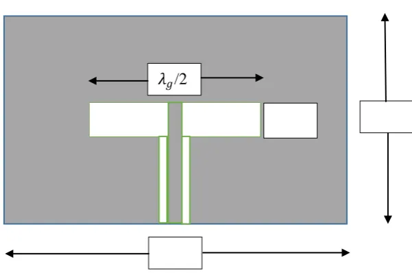
Fig. 1. illustrates the geometry of the proposed CPW fed inductive coupled slot antenna with finite ground plane. The proposed antenna is formed by etching a half wavelength slot 𝜆𝑔/2 located symmetrically with respect to the
center of the CPW fed line,
λg =
c/f
εeff
(1)
where 𝜀𝑒𝑓𝑓 is the effective dielectric constant of CPW fed line and f is the resonant frequency. In the CPW, the
effective dielectric constant is independent of geometry and is equal to the average of dielectric constants of air and of the substrate.
εeff =
εair+εr
2 (2)
CPW fed inductive coupled slot antenna is simulated using RT duroid 5880 substrate with 𝜀𝑟= 2.2, height of the
substrate h= 1.59 mm and loss tangent 0.01 with finite ground plane of size L× W 280 mm × 300 mm. Length of the slot is equal to half wavelength 130mm using equation (1) and the width of the slot is𝜆𝑔/3. CPW feeding technique on
thin substrate,
0.5 ≤ W/h ≤ 2.0 (3)
S
S+2W ≤ 0.4(4)
where S is the strip width and W is the gap width of a CPW fed line as shown in Fig. 1. Size of the strip width S and gap
width W using equation (3) and (4) is 2 mm and 0.5 mm. Analysis of the antenna design parameters, reflection co-efficient, directivity, E-field pattern, H-field pattern can be carried out by varying the width of the slot form 𝜆𝑔/
Fig. 1. Geometry of the proposed antenna fed by CPW. (Dimensions are in mm.) TABLE I. Design parameters of the antenna
Parameters Description Optimal Value
L Length of the antenna 280 mm W Width of the antenna 300 mm l Length of the slot 130 mm w Width of the slot 86.66 mm
Various optimal values of the parameters of the design UWB antenna is obtain from equations (1) to (4) as shown in Table.1. Hence to overcome all drwabacks of cross-talk, dispersion, less gain and undesired radiation pattern is done by proposed design antenna model for desire frequency range using slot on the ground plane with Conductor Backed CPW feeding technique. The gap in the coplanar waveguide is usually very small and supports electric fields primarily concentrated in the dielectric. With little fringing field in the air space, the coplanar waveguide exhibits low dispersion. In order to concentrate the fields in the substrate area and to minimize radiation, the dielectric substrate thickness is usually set equal to about twice the gap width. In CPW a ground plane exists between any two adjacent lines, hence cross talk effects between adjacent lines are very week.
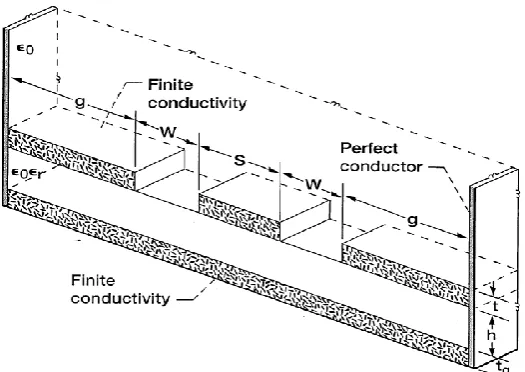
III.STUDY OF CONDUCTOR BACKED CPWANTENNA
CPW feeding technique eliminates all counter problems as it provides low Dispersion, reduces Radiation loss, supports surface mounting of active and passive devices, Bandwidth enhancement, Reduces cross-talk. CPW supports Quasi-TEM mode of propagation hence it has longitudinal components in the direction of propagation. Using
𝜆
𝑔/2
𝜆
𝑔/3
L
Fig. 2. Schematic of conductor Backed Co-planar Waveguide
CPW has ODD mode also called as Co-planar mode where the fields in the two slots are 180 out of phase and an EVEN mode known as coupled slotline mode where the fieldsare in-phase. Since the number of the electric and magnetic field lines in the air is higher than the number of the same lines in the microstrip case, the effective dielectric constant 𝜀𝑒𝑓𝑓 of CPW is typically 15% lower than the 𝜀𝑒𝑓𝑓 for microstrip, so the maximum reachable characteristic
impedance values are higher than the microstrip values. The effect of finite dielectric substrate is almost ignorable if h exceeds 2b = W+2s.
Fig. 3. Schematic of conductor Backed Co-planar Waveguide with finite thickness
IV.SIMULATION RESULTS
Computer Simulation Technology Software is used to simulate the proposed CPW fed slot antenna through inductive coupling. As shown in Table. II the Directivity and Gain of antenna is good with reduced back lobed. Fig. 4 shows the return loss with good impedance matching is observed at 975 MHz frequency with minimum reflection co-efficient.
Fig. 4. Return loss
TABLE II. Result values of the design antenna
Width of Slot Resonant
Frequency Return Loss Directivity Gain
X-Z plane
Y-Z plane 𝜆𝑔/3 975 MHz -20.88 dB 10.3dBi 2.2dB 43.0° 62.6°
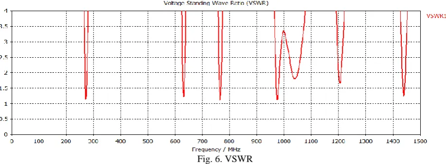
Fig. 6. shows Voltage Standing Wave Ratio.A standing wave in a transmission line is a wave in which the distribution of current, voltage or field strength is formed by the superimposition of two waves of same frequency propagating in opposite direction. The value of VSWR should be between 1 and 2 for efficient performance of an antenna. At frequency 975 MHz its value is nearby 1.
Fig. 6. VSWR
V. CONCLUSION AND FUTURE WORK
CPW-fed proposed antenna exhibit low dispersion, broadside radiation patterns and low cross polarization. The study of feeding techniques plays a vital role in field pattern and impedance matching concept. The dimension of the slot should be less to obtain high efficiency and gain of an antenna. Study of CPW fed inductive coupled slot antenna proposed model shows good efficiency and perfect impedance matching with low cross polarization. Good impedance matching is accomplished with inductive coupled slot antenna at frequency 975MHz with multi band characteristics. Based on these characteristics wide slot inductive coupled antennas fed by CPW with finite ground plane is suitable for navigation systems and in communication applications.
ACKNOWLEDGMET
The authors would like to thank Prof. Dr Nisha Sarwadefrom VJTI Mumbai, for her encouragement and inspiration to work on this current research topic.
REFERENCES.
1. H.-D. Chen, “Broadband CPW-fed square slot antennas with a widened tuning stub,” IEEE Trans. Antennas Proper., vol. 51, no. 4, pp. 1982–1986, Aug. 2003.
2. J.-W. Nia and S.-S. Hong, “A broadband CPW-fed bow-tie slot antenna,” in Proc. IEEE Antennas and Propagation Soc. Int. Sump, vol. 4, pp. 4483–4486, Jun.20–25, 2004.
3. A. A. Drawstring, A. Imani, “Printed wide-slot antenna for wide band applications,” IEEE Trans. Antennas Proper., vol. 56, no. 10, pp. 3097–3102, Oct. 2008.
4. K. P. Ray and Y. Rang, “Ultra wideband printed elliptical monopole antennas,” IEEE Trans. Antennas Proper., vol. 55, no. 4, pp. 1189– 1192, 2007.
5. R. Chair, A. A. Kick, and K. F. Lee, “Ultra wideband coplanar waveguide-fed rectangular slot antenna,” IEEE Antennas Wireless Propag.Lett., vol. 3, pp. 227–229, 2004.
6. B. K. Kormanyos, W. Harokopus, L. Katehi, and G. Rebeiz, “CPW-fed active slot antennas,” IEEE Trans. Microwave Theory Tech., vol. 42, pp. 541–545, Apr. 1994.
8. H. L. Lee, H. J. Lee, J. G. Yook, and H. K. Park, “Broadband planar antenna having round corner rectangular wide slot,” in Proc. IEEE Antennas and Propagation Society Int. Symp., vol. 2, pp. 460–463, Jun. 16–21, 2002.
9. A. U. Bhobe, C. L. Holloway, and M. Piket-May, “CPW fed wide-band hybrid slot antenna,” in Proc. IEEE Antennas Propag. Soc. Int. Symp. Dig, vol. 2, pp. 636–639, Jul. 2000.
10. H.-D. Chen, “Broadband CPW-fed square slot antennas with a widened tuning stub,” IEEE Trans. Antennas Propag., vol. 51, no. 4, pp. 1982–1986, Aug. 2003.
11. B. K. Kormanyos, W. Harokopus, L. Katehi, and G. Rebeiz, “CPW-fed active slot antennas,” IEEE Trans. Microwave Theory Tech., vol. 42, pp. 541–545, Apr. 1994.
12. J.-Y. Sze, C.-I. G. Hsu, and S.-C. Hsu, “Design of a compact dual-band annular-ring slot antenna,” IEEE Antennas Wireless Propag. Lett., vol.6, pp. 423–426, 2007.
13. H. L. Lee, H. J. Lee, J. G. Yook, and H. K. Park, “Broadband planar antenna having round corner rectangular wide slot,” in Proc. IEEE Antennas and Propagation Society Int. Symp, vol. 2, pp. 460–463,Jun. 16–21, 2002.
14. A. U. Bhobe, C. L. Holloway, and M. Piket-May, “CPW fed wide-band hybrid slot antenna,” in Proc. IEEE Antennas Propag. Soc. Int. Symp. Dig,vol. 2, pp. 636–639, Jul. 2000.
BIOGRAPHY
Arpan Shah is Master of Technology inElectronics and Telecommunication Engineering, from VeermataJijabai Technological Institute. Had an experience of two years in teaching profession. Area of interest is High power microwave devices and Antenna design.
Pooja Tendolkar is pursuing Master of Technology in Electronics and Telecommunication Engineering, from Veermata Jijabai Technological Institute. She had an experience of two years in Teaching Profession. Area of interest is Microwave and Antenna design devices.