Department of ECE, Adhiyamaan College of Engineering, Hosur, Tamilnadu, India.
Simulation Analysis of SRAM Cell
Structures Using Low Power Reduction
Techniques
S.Nijantha1, Prof. K.A.Dattathreya2
PG Scholar, Department of ECE, Adhiyamaan College of Engineering, Hosur, Tamilnadu, India1
Professor, Department of ECE, Adhiyamaan College of Engineering, Hosur, Tamilnadu, India2
ABSTRACT : SRAM is one of the common embedded memory for CMOS IC’s and it consists of Bistable
latching circuitry to store a bit. Power consumption and speed are the main factors for designing a chip along with the leakage power. The power consumption and speed of SRAMs are some important issues among a number of factors that provides a solution which describes many designs to minimize the consumption of power. Here this article presents the simulation of 6T,8T and 9T SRAM cells using Low power reduction techniques and develops a modified model which provides the consumer with less costs and reduced power delay product. Simulations have been carried out on 90nm at Tanner EDA tool and the overall circuit is verified using Tanner tool.
KEYWORDS : Various SRAM cells, CMOS Logic ,Low power and VLSI
I. INTRODUCTION
Memory Architecture is Random-access architecture and it is same as Asynchronous design. The SRAM IC is read write (R/W) memory circuit that permits the modification as well as their retrieval. The SRAM IC was developed by CDS IC446, cadence IC design environment. The most popular, full CMOS 6-transistor cell configuration was used to design the SRAM memory array. Fewer advantages are high switching speeds while using full CMOS SRAM configuration.
Department of ECE, Adhiyamaan College of Engineering, Hosur, Tamilnadu, India.
II. LOW POWER SRAM
SRAM cell introduces one control signal transistor for controlling these transistors, the below figure shows the write mode SRAM. Due to one more transistors area is increased in comparison to normal approach. This control transistor uses control select signals which are used to properly control the dissipation in power.
FIGURE 2. 6-T SRAM IN S-EDIT
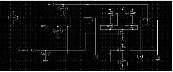
Figure 3 shows the dual-ported cell (8T-SRAM cell) created by adding two transistors; the read operation can be entirely decoupled from the write operation in an 8T cell by sensing the data through a separate read stack controlled by separate read word lines (RWL).
FIGURE 3. 8-T SRAM IN S-EDIT
Department of ECE, Adhiyamaan College of Engineering, Hosur, Tamilnadu, India.
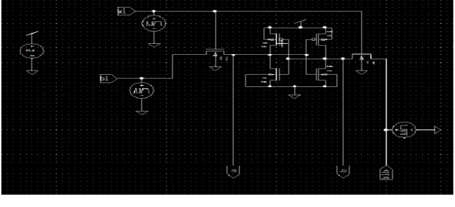
transistors in an SRAM cell.The 9T SRAM Schematic view is shown in the below figure , which is built using Tanner EDA tool using Schematic Edit (S-Edit) to compare their results.
FIGURE 4. 9T SRAM IN S-EDIT
III. SIMULATION ANALYSIS
All the above circuits taken for analysis are simulated using 90nm technology on Tanner EDA tool. To make impartial testing environment all the circuits has been simulated on the same input patterns.
IV. SIMULATION RESULTS
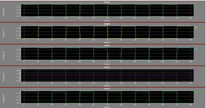
The below figure 5 ,6 and 7 shows output waveforms of different SRAM cells at 90nm technology.
Department of ECE, Adhiyamaan College of Engineering, Hosur, Tamilnadu, India.
FIGURE 6. OUTPUT WAVEFORM OF 8T SRAM
FIGURE 7. OUTPUT WAVEFORM OF 9T SRAM
V. COMPARISON RESULTS
The Power and Delay of different SRAM cells are observed
Design Style No.of transistors Minimum
length(micro meter)
Avg.power
consumption(watts)
Prop. Delay(nano sec)
Department of ECE, Adhiyamaan College of Engineering, Hosur, Tamilnadu, India.
VI. CONCLUSION
The techniques used to reduce the power dissipation is the reduction of the supply voltage. The power dissipation reduction in SRAMs is not considered only to power supply voltage reduction, but also due to operating frequency and temperature. The Average power consumption of 9T is less when compared to 6T and 8T To improve their reliability, the lifetime of battery is a prime concern at the cost of speed. The reduction in the power consumption reduces the problem associated with high temperature and also provides an extra advantage in terms of extended battery life.
REFERENCES
[1] Jawar Singh, Dhiraj K.Pradhan,” A single ended 6T SRAM cell design fro ultra low voltage applications”, IEICE Electronic Express,2008,pp-750-755.
[2] M. Tu et al., “A single-ended disturb-free 9T sub threshold SRAM with cross-point data-aware write word-line structure, negative bit-line, adaptive read operation timing tracing,” IEEE J. Solid-State Circuits, vol. 47, no. 6,Jun. 2012.
[3] A. Teman et al., “A 250 mV 8 kb 40 nm ultra-low power 9T supply feedback SRAM (SF-SRAM),” IEEE J. Solid- State Circuits, vol. 46, no. 11, Nov. 2011.
[4] T. Kim et al., “A voltage scalable 0.26 V, 64 kb 8T SRAM with lowering techniques and deep sleep mode,” IEEE J. Solid-State Circuits, vol. 44, no. 6, Jun. 2009.
[5] D. Jeon et al., “A super-pipelined energy efficiency sub threshold 240 MS/s FFT core in 65 nm CMOS,” IEEE J. Solid-State Circuits, vol. 47, no. 1, pp. 23–34, Jan. 2012.
[6] Y. Sinangil et al., “An embedded energy monitoring circuit for a 128kbit SRAM with body-biased sense-amplifiers,” in Proc. Asian Solid-State Circuits Conf. (A-SSCC), 2012, pp. 69–72.
[7] S. Lütkemeier et al., “A 65 nm 32 b sub threshold processor with 9T Multi-Vt SRAM and adaptive supply voltage control,” IEEE J. Solid- State Circuits, vol. 48, no. 1, pp. 8–19, Jan. 2013.
[8] M.-F. Chang et al., “A Sub-0.3 V Area-efficient L-shaped 7T SRAM with read bit line swing expansion schemes based on boosted read-bit line, asymmetric-vth read-port, offset cell VDD biasing techniques,” IEEE J. Solid-State Circuits, vol. 48, no. 10, pp. 2558–2569, Oct. 2013.
[9] S. Hanson et al., “A low-voltage processor for sensing applications with picowatt standby mode,” IEEE J. Solid-State Circuits, vol. 44, no. 4, pp. 1145–1155, Apr. 2009.