IJEDR1503092 International Journal of Engineering Development and Research (www.ijedr.org) 1
Design and Implementation of Serial Peripheral
Interface Protocol Using Verilog HDL
Fareha Naqvi 1 1 Student
Department of Electronics and Communication Engineering, Alfalah School of Engineering & Technology, Maharishi Dayanand University, Rohtak, Haryana, India
________________________________________________________________________________________________________
Abstract - The objective of this paper is the design and implementation of SPI (serial peripheral interface) master and slave using verilog HDL. The SPI (serial peripheral interface) is a type of serial communication protocol that transfers synchronous serial data in full duplex mode. There are two modes of communications in SPI viz., master and slave. While the master device generates serial clock, the slave devices are allowed with individual slave select lines and the whole design is simulated and synthesized with Xilinx ISE design suite 13.3.1
Keywords - SPI (serial peripheral interface), Verilog HDL.
________________________________________________________________________________________________________ I. INTRODUCTION
Serial to Peripheral Interface (SPI) is a hardware/firmware communications protocol developed by Motorola and later adopted by others in the industry. Sometimes SPI is also called a "four wire" serial bus.The Serial Peripheral Interface or SPI-bus is a simple 4-wire serial communications interface used by many microprocessor/microcontroller peripheral chips that enables the controllers and peripheral devices to communicate with each other. Even though it is developed primarily for the communication between host processor and peripherals, a connection of two processors via SPI is just as well possible. The SPI bus, which operates at full, is a synchronous type data link setup with a Master / Slave interface . Both single-master and multi-master protocols are possible in SPI. The SPI Bus is usually used only on the PCB. The SPI Bus was designed to transfer data between various IC chips, at very high speeds
II. SERIAL PERIPHERAL INTERFACE DESIGN
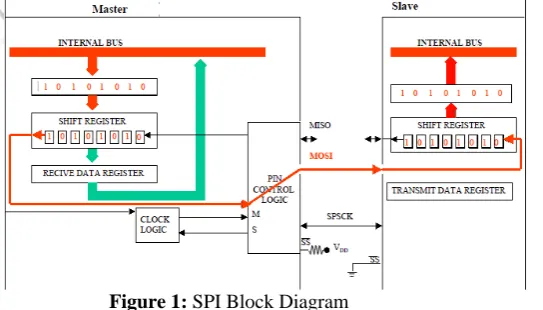
The internal architecture of SPI mainly consists of two modules, master module and slave module as shown in figure 1. The SPI module allows a full duplex, synchronous, serial communication between the MCU and peripheral devices [1]. The main parts of the SPI are status, control and data registers, shifter logic, baud rate generator, master/slave control logic and port control logic. Software can poll the SPI status flags or the SPI operation can be interrupt driven. The SPI module has a total of 4 external pins:
• Master out Slave in (MOSI) - Output data from the master to the inputs of the slaves. • Master in Slave out (MISO) - Output data from a slave to the input of the master.
• Serial Clock (SCLK) - Clock driven by the master to slaves, used to synchronize the data bits.
• Slave Select (SS) - Select signal driven by the master to individual slaves, used to select the target slave [2].
Figure 1: SPI Block Diagram
IJEDR1503092 International Journal of Engineering Development and Research (www.ijedr.org) 2 IV. SLAVE MODE OPERATION
The SPI operates in slave mode when the MSTR bit in SPI .In slave mode, SCK is the SPI clock input from the master, the function of the serial data output pin (MISO) and serial data input pin (MOSI) is determined by the SPC0 bit and BIDIROE bit in SPI Control Register 2. And the SS pin is the slave select input. Before a data transmission the SS pin is connected to ground if the single slave module is used. Once the byte is transferred from the SPI transmit register to the shift register, the SPTE control bit is set indicating that another byte can be written to the SPI transmit data register. The byte of data shifting a bit at time on the MISO pin synchronized with the master serial clock. The master shift register is then automatically transferred to the master SPI receive data register if it is empty. The SPRF control bit is set indicating that the SPI receive register is full and waiting to be read.
V. SPI DATA TRANSMISSION
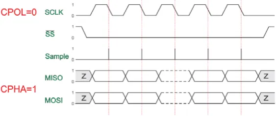
SPI interface allows to transmit and receive data simultaneously on two lines (MOSI and MISO). Clock polarity (CPOL) and clock phase (CPHA) are the main parameters that define a clock format to be used by the SPI bus. Depending on CPOL parameter, SPI clock may be inverted or non-inverted. When clock polarity is set to 1, the idle state for SCLK is high [4].CPHA parameter is used to shift the sampling phase. If CPHA=0 the data are sampled on the leading (first) clock edge. If CPHA=1 the data are sampled on the trailing (second) clock edge, regardless of whether that clock edge is rising or falling.
Clock polarity = 0, Clock phase = 0
Figure 2: Clock polarity = 0, Clock phase = 0
The data must be available before the first clock signal rising. The clock idle state is zero. The data on MISO and MOSI lines must be stable while the clock is high and can be changed when the clock is low. The data is captured on the clock's low-to-high transition and propagated on high-to-low clock transition.
Clock polarity = 0, Clock phase = 1
Figure 3: Clock polarity = 0, Clock phase = 1
The first clock signal rising can be used to prepare the data. The clock idle state is zero. The data on MISO and MOSI lines must be stable while the clock is low and can be changed when the clock is high. The data is captured on the clock's high-to-low transition and propagated on low-to-high clock transition.
IJEDR1503092 International Journal of Engineering Development and Research (www.ijedr.org) 3 Figure 4: Clock polarity = 1, Clock phase = 0
The data must be available before the first clock signal falling. The clock idle state is one. The data on MISO and MOSI lines must be stable while the clock is low and can be changed when the clock is high. The data is captured on the clock's high-to-low transition and propagated on low-to-high clock transition.
Clock polarity = 1, Clock phase = 1
Figure 5: Clock polarity = 1, Clock phase = 1
The first clock signal falling can be used to prepare the data. The clock idle state is one. The data on MISO and MOSI lines must be stable while the clock is high and can be changed when the clock is low. The data is captured on the clock's low-to-high transition and propagated on high-to-low clock transition.
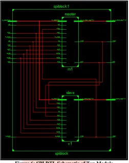
VI. SIMULATION AND RESULTS
IJEDR1503092 International Journal of Engineering Development and Research (www.ijedr.org) 4 Figure 6: SPI RTL Schematic of Top Module
IJEDR1503092 International Journal of Engineering Development and Research (www.ijedr.org) 5 Figure7: SPI Slave to Master Data Transmission
VII. CONCLUSION
The SPI Master and Slave has been implemented using verilog HDL and Xilinx ISE 13.3.1 was used for simulation. The basis of this paper is the focus on data transmission between master and slave modules. We have verified the data in slave device same as the data in the master device and various possible cases of clock polarity and clock phase are verified. Further, we have also done functional verification.
REFERENCES
[1] Motorola Inc., “SPI Block Guide V03.06,” February 2003
[2] Quartus II Handbook version 9.0 volume 5: Embedded Peripherals. Altera SPI core interval time core chapter in volume 5 of the Quartus II.
[3] Digital DNA from Motorola, “SPI Tutorial introduction”.
[4] F.Leens, “An Introduction to I2C and SPI Protocols,”IEEE Instrumentation & Measurement Magazine, pp. 8-13, February 2009.
[5] A.K. Oudjida et al, “FPGA Implementation of I2C and SPI Protocols: A Comparative Study”. Proceedings of the 16th edition of the IEEE International Conference on Electronics Circuits and Systems ICECS, pp. 507 -510, ISBN: 978-1-4244-5091-6,December 13-16 2009, Yasmine Hammamet, Tunisia.