ABSTRACT
PRIYADARSHI, SHIVAM. Dynamic Electrothermal Simulation using Compact Macromodel
of Standard Cells. (Under the direction of Michael B. Steer.)
c
Copyright 2010 by Shivam Priyadarshi
Dynamic Electrothermal Simulation using Compact Macromodel
of Standard Cells
by
Shivam Priyadarshi
A thesis submitted to the Graduate Faculty of
North Carolina State University
in partial fulfillment of the
requirements for the Degree of
Master of Science
Electrical Engineering
Raleigh, North Carolina
2010
APPROVED BY:
DEDICATION
BIOGRAPHY
Shivam Priyadarshi was born on 6th September 1983 in Patna, India. He received the
bachelor degree in Information and Communication Technology from Dhirubhai Ambani
Institute of Information and communication Technology (DA-IICT), India in May 2005.
During his undergraduate he worked as an research intern at Solid State Physics
Labora-tory, New Delhi on MESFET modeling. After graduating from DA-IICT, he worked for
2 years (March 2006- July 2008) as an engineer at Virage Logic (Now Synopsys), Noida.
At Virage Logic, he worked on design and development of Standard Cell libraries and
Memory Compilers.
ACKNOWLEDGEMENTS
I would like to thank my advisor Dr. Michael B. Steer for giving me an opportunity
to work in his supervision. I am deeply grateful for his guidance, motivation, financial
support and above all, for having continuous faith in my work. I would also like to thank
Dr. Paul D. Franzon and Dr. David Schurig for serving on my committee.
My special thanks to Dr. Nikhil Kriplani for helping me understand fREEDA. I am
thankful to Dr. Rhett Davis, Dr. Xun Liu and Dr. Sharon Lubkin for their invaluable
suggestions.
I would like to thank my NCSU colleagues T. Robert Harris, Christopher S. Saunders,
Thorlindur Thorolfsson, Samson Melamed, W. Shepherd Pitts, Daniel Schinke, Dr. Neil
Di Spigna, Suresh Venkatesh, Ojas Ashok Bapat, Harun Demircioglu and Akshay Shyam
Pavagada Raghavendra for brainstorming discussions and feedbacks.
TABLE OF CONTENTS
List of Tables
. . . .
vii
List of Figures
. . . .
viii
Chapter 1 Introduction
. . . .
1
1.1
Motivation . . . .
1
1.2
Original Contribution . . . .
2
1.3
Thesis Organization . . . .
3
Chapter 2 Literature Review
. . . .
5
2.1
Introduction . . . .
5
2.2
Electrothermal Simulation . . . .
5
2.3
Approaches to Electrothermal Simulation . . . .
7
2.4
Summary
. . . .
9
Chapter 3 Dynamic Electrothermal Simulation using Standard Cell
Macro-models
. . . .
10
3.1
Introduction . . . .
10
3.2
Standard Cells based Dynamic Electrothermal Simulation Methodology .
11
3.3
Compact Electrothermal Macromodel of Standard Cells . . . .
14
3.3.1
Inverter Macromodel . . . .
15
3.3.2
NAND Macromodel . . . .
23
3.3.3
NOR Macromodel
. . . .
31
3.3.4
Run time and memory usage comparison . . . .
39
3.3.5
Electrothermal simulation of Full Adder
. . . .
43
3.4
Thermal Network Extractor . . . .
47
3.5
Summary
. . . .
48
Chapter 4 Electrothermal Simulation of Three Dimensional Integrated
Circuit(3DIC)
. . . .
49
4.1
Introduction . . . .
49
4.5
Summary
. . . .
70
Chapter 5 Conclusions
. . . .
71
References
. . . .
73
Appendices
. . . .
77
Appendix A
. . . .
78
A.1 Netlists and Model Parameters . . . .
78
A.1.1 150 nm CMOS EKV model parameters . . . .
78
A.1.2 Netlist for CMOS Inverter DC transfer characteristic . . . .
79
A.1.3 Netlist for CMOS Inverter transient response . . . .
80
A.1.4 Netlist for electrothermal simulation of CMOS Inverter . . .
81
A.1.5 Netlist for 2-Input CMOS NAND DC transfer characteristic
82
A.1.6 Netlist for 2-Input CMOS NAND Transient response . . . .
83
A.1.7 Netlist for electrothermal simulation of 2-Input CMOS NAND
Gate . . . .
85
A.1.8 Netlist for 2-Input CMOS NOR DC transfer characteristic .
86
A.1.9 Netlist for 2-Input CMOS NOR transient response . . . .
87
A.1.10 Netlist for electrothermal simulation of 2-Input CMOS NOR
Gate . . . .
89
A.1.11 Netlist for 8 bit Shift Register . . . .
90
A.1.12 Netlist for Electrothermal Simulation of Frequency
Multiplier-Divider Chain . . . .
92
Appendix B
. . . .
100
B.1 fREEDA Element Codes . . . .
100
B.1.1
CMOS Inverter Macromodel . . . .
100
B.1.2
CMOS Inverter Electrothermal Macromodel . . . .
117
B.1.3
2-Input CMOS NAND Macromodel . . . .
135
B.1.4
2-Input CMOS NAND Electrothermal Macromodel . . . . .
157
B.1.5
2-Input CMOS NOR Macromodel . . . .
180
B.1.6
D-Flipflop Macromodel . . . .
203
B.1.7
XOR Macromodel . . . .
214
B.1.8
Single Tone AC Power Source . . . .
220
LIST OF TABLES
Table 2.1
Thermal-electrical analogy . . . .
7
Table 3.1
Run time and memory usage comparison for macromodel and
transistor-level implementations of CMOS Inverter.
. . . .
19
Table 3.2
Run time and memory usage comparison for macromodel and
transistor-level implementations of 2 input NAND gate. . . .
28
Table 3.3
Run time and memory usage comparison for macromodel and
transistor-level implementations of two input NOR gate. . . .
37
Table 3.4
Number of state variables, run time, and memory usage comparison
between macromodel and transistor-level implementations of various
designs. . . .
42
Table 3.5
Reduction in run time and memory usage due to macromodels,
compared to transistor-level implementations. . . .
42
Table 3.6
Worst case delay errors due to macromodels, compared to
transistor-level implementations. . . .
43
Table 4.1
Power dissipated by different cells present in one tile of the Tier C
and corresponding heat current fitting parameters (rth). . . .
61
Table 4.2
Electrical simulation statistics of complete chain. . . .
63
Table 4.3
Electrothermal simulation statistics of complete chain. . . .
63
Table 4.4
Electrothermal simulation statistics of fastest switching frequency
LIST OF FIGURES
Figure 3.1
Flowchart of proposed dynamic electrothermal simulation
method-ology.The first step is to create electrical macromodel of standard
cells. The second step is to create electrothermal macromodels and
generate thermal netlist. The third step is to build and simulate
target application circuitry using these macromodels. . . .
13
Figure 3.2
CMOS Inverter schematic with various current components
iden-tified. . . .
16
Figure 3.3
Comparison of DC transfer characteristic between macromodel
and transistor-level implementation of CMOS Inverter. . . .
19
Figure 3.4
Comparison of Transient characteristic between macromodel and
transistor-level implementation of CMOS Inverter. . . .
20
Figure 3.5
Schematic of the electrothermal macromodel of the CMOS Inverter. 21
Figure 3.6
Rise in channel temperature of the Inverter macromodel with time. 22
Figure 3.7
Two input CMOS NAND schematic with various current
compo-nents identified. . . .
23
Figure 3.8
Illustration of replacing multiple transistors in parallel by one
equivalent transistor. . . .
26
Figure 3.9
Comparison of DC Transfer characteristic between macromodel
and transistor-level implementation of two Input NAND Gate. . .
28
Figure 3.10 Comparison of transient characteristic between macromodel and
transistor-level implementation of two Input NAND Gate.
. . . .
29
Figure 3.11 Electrothermal macromodel of the NAND gate. . . .
30
Figure 3.12 Rise in channel temperature of the NAND macromodel with time.
31
Figure 3.13 Two input NOR gate schematic with various current components
identified. . . .
32
Figure 3.14 Comparison of DC Transfer characteristic between macromodel
and transistor-level implementation of two input NOR Gate. . . .
36
Figure 3.15 Comparison of transient characteristic between macromodel and
transistor-level implementation of two input NOR Gate.
. . . . .
36
Figure 3.16 Electrothermal macromodel of the 2 input NOR gate.
. . . .
37
Figure 3.17 Rise in channel temperature of the NOR macromodel with time.
39
Figure 3.18 SR Latch schematic built using the NAND macromodel.
. . . .
40
Figure 3.19 D-Flipflop schematic built using the NAND and Inverter
macro-models. . . .
41
Figure 3.20 An 8-bit shift register schematic built using the D-Flipflop
Figure 3.22 Transient temperature of sum node of full adder. . . .
45
Figure 3.23 Transient temperature of carry node of full adder. . . .
46
Figure 3.24 RC network associated to each grid block. . . .
48
Figure 4.1
Floor plan of the 3DIC chip [35]. . . .
51
Figure 4.2
Frequency multiplier-divider chain [35].
. . . .
52
Figure 4.3
Block diagram of one tile. . . .
53
Figure 4.4
The layout of a frequency multiplier. . . .
55
Figure 4.5
The layout of a frequency divider.
. . . .
56
Figure 4.6
Frequency multiplier circuits: (a) frequency multiplier circuit built
using electrothermal NAND macromodels and delay element in
fREEDA; and (b) chain of frequency multipliers built using
elec-trothermal XOR macromodels and delay element in fREEDA. . .
58
Figure 4.7
Frequency divider circuits: (a) frequency divider circuit built
us-ing electrothermal macromodel of D-Flipflop; and (b) chain of
fre-quency dividers. . . .
59
Figure 4.8
Layers extracted in the thermal network from the three-tier layout
structure.
. . . .
62
Figure 4.9
Transient waveform of multiplier-divider junction. . . .
65
Figure 4.10 Transient output of various frequency multipliers. . . .
65
Figure 4.11 Junction temperatures near various frequency multipliers. . . . .
66
Figure 4.12 Thermal profiles: (a) thermal profile of the die showing nine heat
spots each being the multiplier-divider junction of each tile; (b)
hottest point on the die, the multiplier-divider junction of tile (3,3)
1. 67
Figure 4.13 Transient rise in the surface temperature near the hottest point,
obtained from the thermal measurements
2. . . .
68
Chapter 1
Introduction
1.1
Motivation
breakdown and electromigration are accelerated at higher temperature [3]. Furthermore,
increase in temperature requires better heat sink and system cooling solutions which
increases the system cost [4]. So electrothermal issues are affecting the performance
and cost metrics of ICs hence they have become critical in IC design. It is very
impor-tant to address them early in the design phase to save design iterations. This requires a
methodology to perform fast and accurate electrothermal simulation. The electrothermal
simulation can be divided into two parts: static or steady-state simulation and dynamic
simulation. Given a power profile, steady-state simulation can determine the final
tem-perature to which an IC converges as time tends to infinity. Steady-state simulation can
provide a correct estimate of IC temperature only if the power profile does not change
with time or the thermal profile converges well before the power profile starts changing
[5]. Dynamic simulations are required to get the correct estimate of IC temperature when
IC power profile changes with time or varies before the thermal profile converges. It is
also useful in capturing transient variations in the electrical characteristics of signals due
to thermal effects. Furthermore, electrical response might be affected by instantaneous
temperature, causing possible malfunctions which also makes dynamic simulation
nec-essary. Since dynamic simulation is more computationally expensive than steady-state
simulation, it requires a computationally efficient simulation methodology.
1.2
Original Contribution
cuit simulator fREEDA [6]. In these models temperature-dependent electrical parameters
are automatically updated with temperature change. Due to this, the transient changes
in power profile is captured which gives an accurate transient temperature profile. These
macromodels have a reduced number of state variables compared to transistor-level
im-plementation; hence simulations based on these models are faster than transistor-level
simulations. Furthermore, these macromodels are based on transistor equations, hence
produce accurate results. Electrothermal macromodels integrated with a
correspond-ing physically extracted thermal netlist, are used as basic buildcorrespond-ing block for chip-level
dynamic electrothermal simulation. Using this methodology, both transient surface
tem-perature and junction temtem-perature can be simulated which can be a useful tool to study
relationship between them. Power dissipation in different parts of an IC is different and
failure mechanisms of devices depend strongly upon local operating temperature [7]. So
it is very important to locate heat spots due to local power dissipation. Each
electrother-mal standard cell macromodel has a temperature terminal as well as electrical terminals
and by monitoring temperature on these terminals, the local transient temperature
pro-file around that standard cell can be estimated. This information in the design phase
can be very helpful in designing reliable ICs. Application of this methodology is shown
in heat spot modeling of a three dimensional integrated circuit (3DIC).
1.3
Thesis Organization
Chapter 2
Literature Review
2.1
Introduction
In this chapter the basic principle of electrothermal simulation based on the electrical
thermal analogy is presented. The major requirements of electrothermal simulation are
discussed. Two major approaches to electrothermal simulation published in the literature
are described. Furthermore, trade-offs between these two approaches is presented and
reasoned why one of the approaches is used in this work. This gives a background for
standard cell based dynamic electrothermal simulation methodology.
2.2
Electrothermal Simulation
The time dependent three dimensional heat diffusion equation is
ρc
∂T
∂t
=
Q
(
x, y, z, t
) +
k
(
T
)
∂
2T
∂x
2+
∂
2T
∂y
2+
∂
2T
∂z
2where
T
is temperature,
t
is time,
ρ
is material density,
c
is specific heat, and
Q
(x, y, z,
t
) is the rate of heat generation and
k
is temperature dependent thermal conductivity.
The temperature profile can be obtained by solving Eq. 2.1. In Eq. 2.1, the heat
generation rate
Q
(x, y, z, t
) is equivalent to the power consumption in electrical system.
So electrothermal simulation requires close interaction between electrical and thermal
simulations. The electrical simulation is required to obtain information on power
dis-sipation which is fed to the thermal simulation. The thermal simulation is required to
obtain temperature information which is fed to electrical simulation and temperature
dependent device and interconnect parameters are updated accordingly. For a dynamic
electrothermal simulation the following is required:
1. An electrothermal device model. This is a device model in which
temperature-dependent electronic parameters should change according to change in temperature.
2. A fast and accurate dynamic electrical simulation methodology for calculation of
power consumption. Usually electrothermal simulation is required to run for longer
time to see thermal effects, so it is very important to have a fast simulation
method-ology.
3. A fast and accurate thermal simulation methodology. This requires a thermal model
accurately representing the physical structure of chip and a method to solve the
heat Eq. 2.1.
2.3
Approaches to Electrothermal Simulation
There are two main approaches to performing electrothermal simulation of ICs: the
re-laxation method; and the direct method or simultaneous iteration. In the rere-laxation
method electrical and thermal simulations are performed separately and both are
con-nected in an iteration loop [8, 9, 10, 11]. The loop is iterated repeatedly until electrical
and thermal convergence is reached. Usually Spice, ELDO, SABER, or similar circuit
simulator is used for electrical simulation and numerical techniques such as the finite
difference method, the finite element method or the boundary-element method is used
for thermal simulation.
In the direct method [12, 13, 14, 15], an electrical circuit model of a thermal system is
created based on the thermal-electrical analogies shown in Table 2.1 [16]. The electrical
and thermal circuit models are solved simultaneously as if they were one large electrical
circuit model. This effectively converts an electrothermal simulation to pure electrical
simulation.
Table 2.1: Thermal-electrical analogy
Thermal
Electrical
Temperature
T
[K]
Voltage
V
[V]
Heat,
Q
[J]
Charge,
Q
[C]
Heat transfer rate,
q
[W]
Current,
i
[A]
Thermal resistance,
R
T[K/W]
Electrical resistance,
R[V/A]
Thermal capacitance,
C
T[J/K]
Electrical capacitance,
C
[C/V]
Temperature rise ∆T = qR
TVoltage difference ∆V = iR
and voltage (V
). The heat transfer rate corresponds to power dissipation in an electrical
system. This method requires solving the following set of equations using iteration [14]:
Y
E0
0
Y
T H
V
T
=
i
(
V, T
)
q
(
V, T
)
(2.2)
In Eq. 2.2, Y
Ecorresponds to the electrical modified nodal admittance matrix and Y
T Hcorresponds to thermal admittance matrix.
The relaxation method is easier to implement as existing electrical and thermal
sim-ulators can be directly used but convergence of this method is slow in strongly coupled
thermal problems [12, 13]. Furthermore, very fast changes cannot be considered in this
method [14]. The direct method requires a more complex implementation than the
re-laxation approach but is capable of handling very fast changes [17]. The capability of
handling fast changes is very important for dynamic electrothermal simulation; hence in
this work the direct method is used. In the direct method there is the potential problem
of mixing of electrical and thermal currents. This problem has been addressed by
intro-ducing the concept of local reference nodes [18] in a multi physics simulator fREEDA [6].
In this work fREEDA is used for electrothermal simulation which has the capability of
simultaneously solving electrical and thermal circuits.
inte-mainly addressed the transistor-level electrothermal modeling and computationally
ef-ficient modeling of substrate heat conduction for calculating the junction temperature
profile. In this work, a dynamic electrothermal simulation methodology for VLSI circuits
is proposed which is not only computationally efficient and accurate but also has the
capability of estimating the transient profile of both junction temperature and surface
temperature. Furthermore, it is also capable of simulating the local temperature profile
in different parts of VLSI circuits and the transient thermal impact on the electrical
characteristics of signals.
2.4
Summary
Chapter 3
Dynamic Electrothermal Simulation
using Standard Cell Macromodels
3.1
Introduction
3.2
Standard Cells based Dynamic Electrothermal
Simulation Methodology
In today’s IC industry standard cell-based design methodology is a very common method
of designing application specific integrated circuits. Standard cells are like bricks by
which integrated circuits can be built. A standard cell is a group of transistors which
provides a logic function such as Inverter, NAND, NOR, etc, arithmetic function such
as adder, multiplier etc, and storage functions such as flipflop, latch etc. In this work
compact electrical and electrothermal macromodels of these cells are developed. The goal
is to build circuits using these models and perform dynamic electrothermal simulation.
Figure 3.1 shows the methodology proposed in this work. The first step is to create
layout and compact electrical macromodel of standard cells. The layout of standard cell
can be obtained from standard cell libraries on given technology node. The compact
macromodels of standard cells are created for a given technology node which gives the
same functionality as the transistor-level implementation but with fewer state variables.
It is shown in later sections that this gives major run time improvement over a
transistor-level implementation.
at the thermal terminal as current. From the voltage-temperature analogy presented in
Table 2.1, it is obvious that the voltage measured at the thermal terminal will represent
temperature. The thermal network extractor creates a thermal netlist from the layout
based on geometric proximity and material properties.
Layout of Standard Cells
Thermal Network Extractor
Thermal Network
Electrical Input
Compact Electrical Macromodel of Standard Cells
Electrical Output
Electrical Ground Power Supply
Thermal Ground Temperature
Terminal
Instantaneous Power calculated
in Macromodel Electrical
Input
Compact Electrothermal Macromodel of Standard Cells
Electrical Output
Electrical Ground Power Supply
Extracted Thermal Network Electrothermal Macromodel Creation
Build Circuits using Electrothermal Macromodel of Standard Cells integrated
with corresponding Thermal Network
Dynamic Electrothermal Simulation in fREEDA Automatic Dynamic
Updation of Temperature Dependent Device Parameters
+
-Tsnk
3.3
Compact Electrothermal Macromodel of
Stan-dard Cells
Finally, run time and memory usage comparison for macromodel and transistor-level
im-plementations of various designs are presented. This section is concluded by presenting
an electrothermal simulation example of a full adder.
In this work macromodels are implemented in fREEDA using the global modeling
approach [26]. In this approach, the port voltages and port currents are expressed as
functions of state variables and their derivatives as follows:
v
N L(
t
) =
u
x
(
t
)
,
dxdt, ....,
ddtmmx, x
D(
t
)
i
N L(
t
) =
w
x
(
t
)
,
dxdt, ....,
ddtmmx, x
D(
t
)
(3.1)
where
v
N L(t) and
i
N L(t) are vectors of port voltages and currents,
x
(t) is the vector of
state variable and
x
D(t) is vector of time delayed state variable. The derivatives are
cal-culated by automatic differentiation packages integrated in fREEDA. The characteristic
equations of devices used in the model define the functions given in Eq. 3.1.
3.3.1
Inverter Macromodel
The schematic of the CMOS Inverter with various current components is shown in
Fig-ure 3.2. In this macromodel electrical characteristic equations are formulated in terms
of 3 state variables as follows:
x
[0] =
V DD,
x
[1] =
V
in,
and
x
[2] =
V
out.
(3.2)
VDD
GND
IN OUT
I
inI
outI
VDDI
PI
NFigure 3.2: CMOS Inverter schematic with various current components identified.
equation of devices shown Figure 1 are based on EKV MOSFET [27] formulation. In the
EKV formulation, the drain, gate, and source voltages of the transistor are referenced
with respect to bulk. In this macromodel implementation these bulk- referenced voltages
are represented in terms of state variables given in Eq. 3.2 assuming source and bulk are
at same potential.
V
db N=
x
[2]
V
db P=
x
[2]
−
x
[0]
V
gb N=
x
[1]
In fREEDA [6], it is assumed that a current source is attached to each terminal and
pump-ing current inside the terminals. The current enterpump-ing in each terminal is composed of
static current i.e. DC current and dynamic current. The dynamic current can be
mod-eled using nonlinear capacitances but their calculation is complex. Hence the dynamic
current is modeled using charges associated with the ports. The following is the gate
current formulation:
I
in=
dQ
gNdt
+
dQ
gPdt
.
(3.4)
In Eq. 3.4,
Q
gNand
Q
gPare gate charge of NMOS and PMOS respectively. DC
current entering in gate is assumed to be zero. The output current is calculated as
I
out=
I
N+
I
P+
dQ
dNdt
+
dQ
dPdt
.
(3.5)
In Eq. 3.5,
I
Nand
I
Pare DC drain current of NMOS and PMOS respectively.
Q
dNand
Q
dPare drain charge of NMOS and PMOS respectively. The current entering from
the terminal VDD is given by:
I
V DD=
−
(
I
p+
dQ
V DDdt
)
.
(3.6)
where
Q
V DDis the source charge of PMOS.
Based on the EKV MOSFET [27] model equations, the static current and charges in
Eq. 3.4,Eq. 3.5,and Eq. 3.6 are formulated as functions of bulk referenced drain, and gate
voltage of NMOS and PMOS (see Eq. 3.3):
The time derivative of charge is partitioned in to multiplication of voltage derivative
of charge and time derivative of voltage. The time derivatives of voltages are calculated
using the TimeDomainSV class of fREEDA. This class provides time differentiation
meth-ods and it is also used to exchange information between an element and a state variable
based time domain analysis. The voltage derivative of charge is calculated using Sacado
[28], an automatic differentiation package.
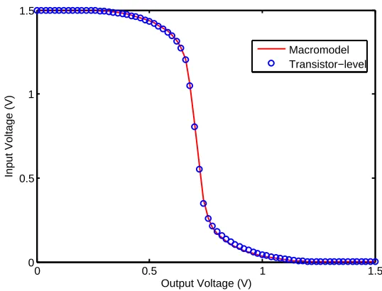
0 0.5 1 1.5 0
0.5 1 1.5
Output Voltage (V)
Input Voltage (V)
Macromodel Transistor−level
Figure 3.3:
Comparison of DC transfer characteristic between macromodel and
transistor-level implementation of CMOS Inverter.
The run time and memory usage of the macromodel and transistor level
implemen-tations are compared by running a transient simulation for 100
µ
s with a step size of 1
ns. The state variable-based fixed time step time marching transient analysis method is
used for these simulations. The simulations are performed on a 3 GHz Intel Xeon server
having 32 GB of RAM. Table 3.1 summarizes the results.
Table 3.1: Run time and memory usage comparison for macromodel and transistor-level
implementations of CMOS Inverter.
Implementation
# of State Variables
Run Time (sec)
% of RAM used
Compact Macromodel
3
6
0.2
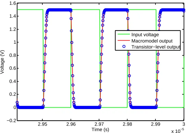
2.95 2.96 2.97 2.98 2.99 3 x 10⁻⁵ −0.2
0 0.2 0.4 0.6 0.8 1 1.2 1.4 1.6
Time (s)
Voltage (V)
Input voltage Macromodel output Transistor−level output
Figure 3.4: Comparison of Transient characteristic between macromodel and
transistor-level implementation of CMOS Inverter.
In the electrical macromodel described above, the temperature is specified as a model
parameter and is kept constant throughout the simulation. So, the device equations
are evaluated for a constant temperature and temperature change due to self heating is
not handled. To include thermal effects, the electrothermal macromodel of inverter is
created from its electrical macromodel by introducing temperature as an additional state
variable.
Thermal Ground
Iheat
VDD
GND
IN OUT
Iin Iout
IVDD
IP
IN
Thermal Network
Temperature
+
-Tsnk
Figure 3.5: Schematic of the electrothermal macromodel of the CMOS Inverter.
parameters include the long channel threshold voltage, bulk fermi potential, mobility,
longitudinal critical field, and the second impact ionization coefficient. As
x
[3] changes,
these parameters are automatically updated accordingly.
I
heatin Figure 3.5 is the heat
current flowing into the thermal network which is equal in magnitude to the power
dis-sipated in electrical macromodel.
I
heatis calculated as following:
I
heat=
−
((
I
N+
dQ
dNdt
)
V
ds N+ (
I
P+
dQ
dPdt
)
V
ds P)
.
(3.9)
where
V
ds Nand
V
ds Pare drain-source voltage of NMOS and PMOS respectively.
I
heatincludes all both dynamic and static power dissipation.
channel temperature with time.
0 0.1 0.2 0.3 0.4 0.5 0.6 0.7 0.8 0.9 1
x 10−3 −0.01
0 0.01 0.02 0.03 0.04 0.05 0.06
Time (s)
Temperature Rise (K)
3.3.2
NAND Macromodel
The schematic of the NAND macromodel with various current components is shown in
Figure 3.7. In this macromodel the electrical characteristic equations are formulated in
terms of 4 state variables as follows:
x
[0] =
V DD,
x
[1] =
V
in1,
x
[2] =
V
in2,
and
x
[3] =
V
out.
(3.10)
VDD
IN1
IN2
OUT
GND
I
P1I
P2I
VDDI
N+i
nI
outP1 P2
N1
N2
I
IN1I
IN2 xN1+N2
The complete transistor-level implementation requires 12 state variables, 3 for each
transistor. So the number of state variable in the macromodel is 1/3 of the state variables
required for transistor-level implementation.
The bulk referenced drain, gate and source voltages of each transistor are represented
in terms of state variables given in Eq. 3.10. The PMOS voltages are given by Eq. 3.11
assuming source and bulk are at same potential.
V
db P1=
x
[3]
−
x
[0]
,
V
gb P1=
x
[1]
−
x
[0]
,
V
sb P1= 0
,
V
db P2=
x
[3]
−
x
[0]
,
V
gb P2=
x
[2]
−
x
[0]
,
and
V
sb P2= 0
.
(3.11)
In the NAND schematic, see Figure 3.7, the ground path has two NMOS transistors
in series. In the macromodel formulation the internal node ‘x’ is eliminated by replacing
the two NMOS transistors in series with a single equivalent transistor. The
transcon-ductance of the equivalent transistor is given by
β
1β
2/(
β
1+
β
2)
where
β
1and
β
2are the
transconductances of individual NMOS transistors. This equivalent transconductance is
used for calculating the equivalent DC drain current
I
Nshown in Figure 3.7. The smaller
equations summarize the above formulation.
if (
x
[1]
> x
[2])
V
db N2=
x
[3]
V
gb N2=
x
[2]
V
sb N2= 0
β
eq=
β
1β
2/
(
β
1+
β
2)
i
n=
dQdtdN2.
else
V
db N1=
x
[3]
V
gb N1=
x
[1]
V
sb N1= 0
β
eq=
β
1β
2/
(
β
1+
β
2)i
n=
dQdtdN1.
(3.12)
where
i
nis dynamic current flowing through NMOS transistors.
Q
dN1and
Q
dN2are the
drain charges of N1 and N2 respectively.
N1 N2 Nn-1 Nn N1+N2+…..+Nn-1+Nn
βeq=β1+β2+---+βn-1+βn
Figure 3.8:
Illustration of replacing multiple transistors in parallel by one equivalent
transistor.
The output current
I
outshown in Figure 3.7 has DC components and dynamic
com-ponents. DC components are calculated using the EKV MOSFET [27] model equations
and the dynamic currents are calculated by taking the time derivative of corresponding
nodal charge.
I
outis given by
I
out=
I
P1+
I
P2+
I
N+
i
n+
dQ
dP1dt
+
dQ
dP2dt
.
(3.13)
In Eq. 3.13,
I
P1and
I
P2are DC drain currents flowing through P1 and P2 respectively.
I
Nis the equivalent DC drain current flowing through the NMOS series chain;
i
nis the
equivalent dynamic drain current flowing through the NMOS series chain which is given
by Eq. 3.12; and
Q
dP1and
Q
dP2are the drain charges of P1 and P2 respectively. The
current entering the VDD terminal is given by
I
V DD=
−
I
P1+
I
P2+
dQ
V DDdt
.
(3.14)
In Eq. 3.15,
Q
gN1and
Q
gN2are the gate charges of N1 and N2 respectively. Similarly,
Q
gP1and
Q
gP2are the gate charges of P1 and P2 respectively. The DC current entering
in each input terminal is assumed to be zero. The DC current and charge in Eq. 3.12,
Eq. 3.13, Eq. 3.14, and Eq. 3.15 are formulated as functions of the state variables given
in Eq. 3.11:
{
I
P1, I
P2, I
N, Q
V DD, Q
dP1, Q
dP2, Q
dN1, Q
dN2, Q
gP1, Q
gP2, Q
gN1, Q
gN2}
=
f
(
x
[0]
, x
[1]
, x
[2]
, x
[3])
.
(3.16)
0 0.5 1 1.5 0
0.5 1 1.5
Output Voltage (V)
Input Voltage (V)
Macromodel Transistor−level
Figure 3.9:
Comparison of DC Transfer characteristic between macromodel and
transistor-level implementation of two Input NAND Gate.
The run time and memory usage of the macromodel and transistor level
implemen-tations are compared by running a transient simulation for 100
µ
s with a step size of 1
ns. The state variable-based fixed time step time marching transient analysis method is
used for these simulations. The simulations are performed on a 3 GHz Intel Xeon server
having 32 GB of RAM. Table 3.2 summarizes the results.
Table 3.2: Run time and memory usage comparison for macromodel and transistor-level
implementations of 2 input NAND gate.
Implementation
# of State Variables
Run Time (sec)
% of RAM used
Compact Macromodel
4
9
0.3
2.8 2.9 3 3.1 3.2 3.3 3.4 3.5
x 10−5 −0.2
0 0.2 0.4 0.6 0.8 1 1.2 1.4 1.6
Time (s)
Output Voltage (V)
Macromodel Transistor−level
Figure 3.10: Comparison of transient characteristic between macromodel and
transistor-level implementation of two Input NAND Gate.
ature as an additional state variable. The electrothermal macromodel of the NAND has
two additional terminals: Temperature and Thermal Ground. It is shown in Figure 3.11.
The thermal network shown in Figure 3.11 represents the physical structure of the
NAND gate. It can be directly extracted from the layout using numerical techniques or
a compact thermal model can be developed to represent this structure.
if (
x
[1]
> x
[2])
I
heat=
−
((
I
N+
i
n)
∗
V
ds N2+ (
I
P1+
dQdtdP1)
∗
V
ds P1+ (
I
P2+
dQdtdP2)
∗
V
ds P2)
.
else
VDD
IN1
IN2
OUT
GND
IP1 IP2
IVDD
IN+in
Iout
P1 P2
N1
N2 IIN1
IIN2 x
N1+N2
Thermal Network Temperature
Iheat
Thermal Ground
+ -Tsnk
Figure 3.11: Electrothermal macromodel of the NAND gate.
0 0.2 0.4 0.6 0.8 1
x 10−3 0
0.05 0.1 0.15 0.2 0.25
Time (s)
Temperature Rise (K)
Figure 3.12: Rise in channel temperature of the NAND macromodel with time.
3.3.3
NOR Macromodel
The schematic of the NOR macromodel with various current components is shown in
Figure 3.13
The electrical characteristics of the NOR gate is formulated using following 4 state
variables:
x
[0] =
V DD,
x
[1] =
V
in1,
x
[2] =
V
in2, and
x
[3] =
V
out.
(3.18)
GND
VDD
IN1
IN2
OUT P1
P2
N1 N2
I
IN1I
IN2I
N1I
N2x
I
outI
P+i
pI
VDDFigure 3.13: Two input NOR gate schematic with various current components identified.
in this macromodel is 1/3 of the state variables required for transistor-level
implementa-tion.
V
gb N1=
x
[1]
,
V
db N1=
x
[3]
,
V
sb N1= 0
,
V
gb N2=
x
[2]
,
V
db N2=
x
[3]
,
and
V
sb N2= 0
.
(3.19)
The NOR gate has two PMOS transistors in series in the VDD path as shown in
Fig-ure 3.13. In the macromodel formulation, the internal node ‘x’ is eliminated by replacing
the two PMOS transistors in series with a single equivalent transistor. The
transcon-ductance of the equivalent transistor is given by
β
1β
2/(
β
1+
β
2)
where
β
1and
β
2are the
transconductances of individual PMOS transistors. This equivalent transconductance is
used for calculating equivalent DC drain current
I
Pshown in Figure 3.13. The bigger
if (
x
[2]
> x
[1])
V
db P2=
x
[3]
−
x
[0]
V
gb P2=
x
[2]
V
sb P2= 0
β
eq=
β
1β
2/
(
β
1+
β
2)i
p=
dQdtdP2.
else
V
db P1=
x
[3]
−
x
[0]
V
gb P1=
x
[1]
V
sb P1= 0
β
eq=
β
1β
2/
(
β
1+
β
2)
i
p=
dQdtdP1.
(3.20)
The output current
I
outshown in Figure 3.13 has DC components and dynamic
components. The DC components are calculated using the EKV mosfet model equations
and dynamic currents are calculated by taking the time derivative of corresponding nodal
charge.
I
outis given by Eq. 3.21.
I
out=
I
N1+
I
N2+
I
P+
i
p+
dQ
dN1dt
+
dQ
dN2dt
.
(3.21)
I
V DD=
−
I
P+
dQ
V DDdt
.
(3.22)
where
Q
V DDis taken as source charge of P2 if x[2]
>
x[1], otherwise it is taken as source
charge of P1.
The currents entering the input terminals are formulated as following:
I
IN1=
dQgN1
dt
+
dQgP1dt
I
IN2=
dQgN2
dt
+
dQgP2dt
.
(3.23)
whereQ
gN1and
Q
gN2are the gate charges of N1 and N2 respectively. Similarly,
Q
gP1and
Q
gP2are the gate charges of P1 and P2 respectively. The DC current entering in
each input terminal is assumed to be zero.
0 0.5 1 1.5 0
0.5 1 1.5
Output Voltage (V)
Input Voltage (V)
Macromodel Transistor−level
Figure 3.14:
Comparison of DC Transfer characteristic between macromodel and
transistor-level implementation of two input NOR Gate.
2.1 2.2 2.3 2.4 2.5 2.6 2.7 2.8 2.9 3
x 10−5 −0.2
0 0.2 0.4 0.6 0.8 1 1.2 1.4 1.6
Time (s)
Output Voltage (V)
Macromodel Transistor−level
Table 3.3: Run time and memory usage comparison for macromodel and transistor-level
implementations of two input NOR gate.
Implementation
# of State Variables
Run Time (sec)
% of RAM used
Compact Macromodel
4
10
0.3
Transistor Level
12
42
0.5
used for these simulations. The simulations are performed on a 3 GHz Intel Xeon server
having 32 GB of RAM. Table 3.3 summarizes the results.
The electrothermal macromodel of the NOR gate is shown in Figure 3.16. It was
created from the electrical macromodel by introducing temperature as an additional state
variable. All temperature-dependent device parameters are expressed as function of this
state variable. As temperature changes these parameters get updated automatically.
GND VDD
IN1
IN2
OUT P1
P2
N1 N2
IIN1
IIN2
IN1 IN2
x
Iout
IP+ip
IVDD
Thermal Network Temperature
Iheat
Thermal Ground
+ -Tsnk
I
heatis given by Eq. 3.24
if (
x
[2]
> x
[1])
I
heat=
−
((
I
P+
i
p)
∗
V
ds P2+ (
I
N1+
dQdtdN1)
∗
V
ds N1+ (
I
N2+
dQdtdN2)
∗
V
ds N2)
.
else
I
heat=
−
((
I
P+
i
p)
∗
V
ds P1+ (
I
N1+
dQdtdN1)
∗
V
ds N1+ (
I
N2+
dQdtdN2)
∗
V
ds N2)
.
(3.24)
where
V
ds N1,
V
ds N2,
V
ds P1, and
V
ds P2are drain source voltage of N1, N2, P1 and P2
respectively.
0 0.1 0.2 0.3 0.4 0.5 0.6 0.7 0.8 0.9 1 x 10⁻³ 0
0.05 0.1 0.15 0.2 0.25 0.3 0.35
Time (s)
Temperature Rise (K)
Figure 3.17: Rise in channel temperature of the NOR macromodel with time.
3.3.4
Run time and memory usage comparison
In this subsection the run time and memory usage comparison between electrical
simu-lations using macromodel and transistor-level implementations are presented. For these
comparisons, complex cells such as SR-Latch, D-Flipflop, and 8-bit shift register were
created using basic cells presented in Section 3.3. It is observed that for the large scale
circuits, the macromodel implementation gives major run time improvement. The
per-centage deviation of macromodel delay from transistor-level delay is also presented.
Figure 3.18 shows the schematic of an SR-Latch built using NAND macromodel. It
has 8 state variables whereas an equivalent transistor-level implementation requires 24
state variables. So the number of state variables is reduced by a factor of 3 which reduces
the run time by a factor of 4.
NAND
NAND
Q
Q
R
S
Figure 3.18: SR Latch schematic built using the NAND macromodel.
NAND
NAND
NAND
NAND
NAND
NAND NAND
NAND
Inverter D
CLK
Q
Q
Figure 3.19: D-Flipflop schematic built using the NAND and Inverter macromodels.
Q Q
D
CLK
Q Q
D
CLK
Q Q
D
CLK
Q Q
D
CLK
Q Q
D
CLK
Q Q
D
CLK
Q Q
D
CLK
Q Q
D
CLK
Input
CLK
Figure 3.20: An 8-bit shift register schematic built using the D-Flipflop macromodels.
stan-dard cells. Table 3.5 and Table 3.6 show that dynamic simulation using macromodel
of standard cells, run faster and consume lesser memory than transistor-level simulation
while maintaining the accuracy in an acceptable limit.
Table 3.4: Number of state variables, run time, and memory usage comparison between
macromodel and transistor-level implementations of various designs.
# of State Variable
Run time
% of RAM used
Design
Macro.
Trans.
Macro.
Trans.
Macro.
Trans.
Inverter
3
6
6
s9 s
0.2
0.3
2-input NAND gate
4
12
9 s
37 s
0.3
0.5
2-input NOR gate
4
12
10 s
42 s
0.3
0.5
SR-Latch
8
24
19 s
1 m 16 s
0.4
0.7
D-Flipflop
35
99
3 m 16 s
28 m 2 s
0.5
1.0
8-bit Shift Register
280
792
2.5 h 29 m
90 h 50 m
2.4
6.6
Table 3.5: Reduction in run time and memory usage due to macromodels, compared to
transistor-level implementations.
Design
Reduction in run time
Reduction in memory usage
Inverter
1.5x
1.5x
2-input NAND
4.11x
1.62x
2-input NOR
4.2x
1.62x
SR-Latch
4x
1.75x
D-Flipflop
8.58x
2.00x
Table 3.6:
Worst case delay errors due to macromodels, compared to transistor-level
implementations.
Design
Delay error (%)
Inverter
0.01
2-input NAND
0.32
2-input NOR
0.36
SR-Latch
0.54
D-Flipflop
0.62
8-bit Shift Register
0.80
3.3.5
Electrothermal simulation of Full Adder
The electrothermal schematic of full adder is shown in Figure 3.21.
The full adder
functionality is realized using 9 electrothermal NAND macromodels. The temperature
terminal of each electrothermal NAND macromodel is connected to a thermal heat sink
through a 10 Ω resistor.
3.4
Thermal Network Extractor
Grid Block