Realizing the potential of polyethylene oxide as new positive tribo-material:
over 40 W/m
2high power flat surface triboelectric nanogenerators
Peng Dinga,†, Jinkai Chena,†, Umar Farooqa, Pengfei Zhaob, Navneet Soinb, Liyang Yuc*, Hao Jina, Xiaozhi Wanga, Shurong Donga and Jikui Luoc,b*
aColl. of Info. Sci. & Electron. Eng., Zhejiang University, 38 Zheda Road, Hangzhou 310027, China. bInst. of Renew. Energy & Environ. Technol., Bolton University, Deane Road, Bolton BL3 5AB, UK cKey Lab of RF Circuits and Systems, Hangzhou Dianzi University, Hangzhou 310018, China
†
These authors contributed equally to the work.
*Corresponding authors emails: [email protected], [email protected]
Abstract:
The on-going research into the negative tribo-materials has led to significant improvements in the performance of triboelectric nanogenerators (TENGs), however, very little attention has been paid for positive tribo-materials. This work reports on the use of poly(ethylene oxide) (PEO) as the positive tribo-material for the fabrication of TENGs and shows that PEO has much higher positive tribo-polarity than the existing choice of polyamide-6 (PA6). A 2 × 2 cm2 TENG comprising of spin-coated flat PEO and polydimethylsiloxane (PDMS) films produces a voltage of up to 970 V, a current density of 85 mAm-2, and a power of ~40 Wm-2 under a 50 N contact force. Comparatively, the PA6/PDMS TENG only produces 630 V, 30 mAm-2, and a power of ~18 Wm-2, showing the remarkable property of the PEO as the positive tribo-material. The results are further supported by the contact potential difference between PEO (1.26 V) and PA6 (0.87 V) obtained using Kelvin Probe Force microscopy. Furthermore the triboelectric behavior of PEO is explained in the context of the positively charged oxygen functional groups and the lower work function of PEO as compared to PA6. The work thus expands the current portfolio of materials used for triboelectric nanogenerators with great prospects.
Keywords: triboelectric nanogenerator, poly(ethylene oxide), polyimide (PA6 Nylon), high surface
1. Introduction
With the development of intelligent electronic devices, such as smart portable/wearable devices, wireless sensor networks and so on, renewable and sustainable power sources, that can be utilized to build battery-free systems, are becoming increasingly important. Since the power consumption of these electronic systems is of hundreds of microwatts to tens of milliWatt levels, it is possible to power these electronic systems by harvesting ubiquitous ambient small-scale waste mechanical energy. Microgenerators based on piezoelectric [1-3], electromagnetic [4], pyroelectric [5] effects have been intensively studied and exploited for
such applications. Triboelectric nanogenerators (TENGs), invented by Wang et al in 2012 [6],
can convert the available mechanical energy such as vibration [7], wind [8, 9] and waves [10, 11] into usable electric energy, have gained great attention since then owing to their very high power output, excellent energy conversion efficiency and cost-effectiveness.
The TENGs have three basic operating modes: two electrode contact [12], single electrode contact [13] and sliding modes [14], with the first one being the preferred one owing to its simple architecture and high performance. The contact mode TENGs typically consist of two
insulators with electric polarities far apart in the triboelectric series [15], i.e. upon contact and
subsequent separation, one material has a high ability to donate electrons (hereafter called as the positive tribo-material), while the other material has a high ability to gain electrons (called as the negative tribo-material). Current efforts for the development of TENG
technology mainly focus on the enhancement of the output power via an increase in the
surface charge density. To this effect, the recent approaches rely on: (i) judicious selection of triboelectric materials, (ii) modification of tribo-materials, for instance, surface patterning
with micro-/nano-structures [16], chemical surface functionalization [17], and
the cost of the TENGs. For instance, the nano/micro-structured surfaces and injected charges tend to deteriorate with operation due to damage of the microstructures and thus may not provide the required stability and reliability of the devices, whereas the hybrid structures have the potential for high conversion efficiency [26], but are yet to achieve satisfactory results. Consequently, the selection of the optimal materials with high electron affinity difference is the simplest and most effective way to improve the performance of TENGs, but is currently restricted by the limited choices of existing materials.
Vigorous investigations have shown that polydimethylsiloxane (PDMS), polyvinylidene fluoride (PVDF) and polytetrafluoroethylene (PTFE) are among the best negative tribo-materials for high performance TENGs owing to their strong negative electron affinity [27-29]. On the contrary, not much attention has been paid to the selection of positive tribo-materials, even though they are equally important as the negative tribo-materials for enhancing the surface charge density and subsequent power density. It is clear from the triboelectric series, there are only very limited choices for positive insulator tribo-materials and mostly metals such as aluminum (Al) and copper (Cu) have been used as positive tribo-materials [30-32]. However, these metals do not rank high in triboelectric series in their ability to donate electrons. For example, flat surfaced Cu/PTFE TENG shown in the literature
was shown to have a charge density of 40 μCm-2 only [33], much smaller than those of other
reported TENGs. Several other positive triboelectric insulator materials have been employed to construct TENGs, such as silk [34], carbon nanotubes (CNTs) [35], glass [36] and polyamide-6 (PA6, Nylon) with varying degrees of success [37]. The silk/PET TENG
obtained a maximum peak power density of only 10 mWm-2, while the CNTs/PDMS TENG
produced about 5 Wm-2 which was mainly attributed to the high surface area of CNT arrays
[35]. Among the positive triboelectric insulator materials, PA6 is regarded as the best choice for making high performance TENGs as it has a strong positive tribo-polarity in triboelectric series. Our earlier works utilizing PA6 as the positive tribo-material against poly(vinylidene
fluoride), PVDF, was shown to perform excellently, providing an open-circuit voltage, VOC,
of 520 V, and a short-circuit current density, JSC, of 2.7 mAm-2 [37]. Similarly, in this work,
using PA6 against a PDMS counter-surface, the PA6/PDMS TENG was shown to provide a
with an effective maximum peak power density of 18 Wm-2.It is apparent that the search for positive materials for TENGs is lagging far behind that of negative tribo-materials and thus warrants the question: is there any other low-cost material which possesses higher positive polarity for enhancing the power output and surface charge density of TENGs?
Polyethylene oxide (PEO) is a synthetic, low-cost commodity polymer which is also bio-compatible and water-soluble [38]. Here, we report for the first time on the use of pristine PEO films as the positive tribo-material to fabricate high performance TENGs in combination with PDMS. Relying on a simple spin-coating process without the added complication of micro/nano-fabrication process, we demonstrate PEO/PDMS TENGs with a peak-to-peak
VOC of 970 V, a JSC of 85 mAm-2 (corresponding a charge density of 154 μCm-2), and a peak
power density of ~40 Wm-2, significantly higher than those of CNTs/PDMS and PA6/PDMS
TENGs, and is one of the best performances reported yet for TENGs comprising of pristine flat membrane structures. The higher positive electronic affinity of the PEO films as compared to that of PA6 is further verified by Kelvin probe force microscopy (KPFM), as the contact potential difference (CPD) values for PEO and PA6 are 1.26 V and 0.87 V, respectively. And the voltage and current density of the PEO/PDMS TENG increase with the increase in contact force, movement frequency and spacer distance. Considering the desirable properties of water solubility and bio-compatibility, we believe that the PEO based TENG devices have broad application prospects in implantable and bio-compatible electronic devices besides their use as high performance energy harvesters for conventional portable electronics.
2. Fabrication and experimental setup
2.1. Fabrication of triboelectric nanogenerators
Corning Co. Ltd.) solution was prepared by mixing the elastomer and cross-linker in a 10:1 ratio (w/w). The obtained solution was degassed prior to being spun onto the Ni electrode, initially at 500 rpm (rotations per minute) for 10 sec, followed by 1200 rpm for 10 sec. The as-obtained PDMS film was then thermally cured on a cleanroom paper on a hot plate at 105 °C for 40 min (note the temperature of the acrylic plate is lower than 105°C, and no deformation of the acrylic plate was observed). The thickness of the resulting PDMS films was measured to be ~140 μm, as confirmed using the profilometer.
PEO powders with different molecular weights (Mw) were purchased from Shanghai EKEAR
Biological Technology Co. Ltd (China). The samples prepared using PEO of molecular
weight (Mw) of 100000, 600000, 3000000 g.mol-1, are hereafter designated as PEO10,
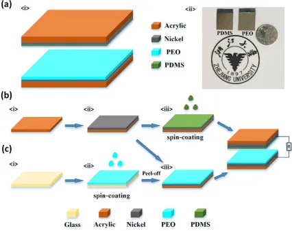
PEO60, PEO300, respectively. The PEO powders were dissolved in deionized (DI) water at different mass concentrations of 12% for PEO10, 9% for PEO60 and 2% (w/w) for PEO300 owing to the fact that polymers with different molecular weights have different viscosity levels [38]. The resulting PEO solutions were spun on glass substrates at different rotation speeds between 500 – 1500 rpm for 10 sec to obtain the films with different thicknesses and subsequently dried in an oven at 55 °C for 3 hr. Finally, the dried PEO films were peeled off from the glass substrate and attached to adhesive Ni electrodes, as shown in Fig. 1(c).
For comparison, PA6/PDMS TENGs were also fabricated. The PA6 (pellets obtained from Rhodia Ltd.) membranes were prepared by a phase-inversion process, in accordance with
earlier reports by Soin et al [37]. The obtained PA6 membranes with a thickness of ~150 µm
were glued to the Ni conductive tapes to assemble the TENGs.
2.2. Experimental setup and Characterization
A dynamic fatigue tester system (Popwil Model YPS-1) was utilized to characterize the TENGs by controlling the contact force, frequency and spacer distance of two substrates of different materials. An oscilloscope (Tektronix MDO3022) with an internal load resistance of 100 MΩ was used to test the open-circuit voltage. The short circuit current was measured
TENGs was connected to the positive side of the oscilloscope and picoammeter, with that of PDMS side of TENGs grounded. The measurements were conducted when the output performance of TENGs reached stable. In our experiments, the dynamic fatigue tester system contacts the two plates closely under a fixed force before dynamic contact and separation, which guarantees a full contact between them. This process reduces the time to reach the stable output, which is typically less than 100 cycles. In a typical test, the plate consisting of the positive tribo-material was moved vertically to make contact with the plate with negative
tribo-material. The active area of TENGs characterized is 2 × 2 cm2, unless specified. The
Kelvin Probe Force Microscopy (KPFM) measurements were performed using the KPFM mode in an atomic force microscopy (AFM) system (Veeco Dimension 3100) with a Pt-coated Si probe. The measurements were carried out at oscillation amplitude of 3 V, resonance frequency of 150 kHz at a distance of 20 nm between the probe tip and sample. The Fourier Transform infrared spectroscopy (FTIR) spectra of PEO and PA6 samples were
obtained using a Bruker TENSOR II at a nominal resolution of ±2 cm-1 for a total of 64 scans
and the data was analyzed using the vendor-provided software, OPUS.
3. Results and Discussion
3.1. Performance of TENGs with different materials
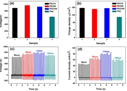
Using PEO films of various thicknesses and molecular weights, we have evaluated the output performance of the PEO/PDMS TENGs to gain an understanding of the role of physico-chemical properties of PEO on its triboelectric properties. Furthermore, to assess its performance against the benchmark PA6 material, a comparison of PA6/PDMS and PEO/PDMS TENGs was carried out at a fixed working condition of 50 N impact force, 5 Hz working frequency and 4 mm spacer distance, with the results presented in Fig 2. Considering
the effect of molecular weight first, Figs. 2(a) and (b) exhibit the peak-to-peak VOC and
charge density of the TENGs with PEO films with different molecular weights but
approximately similar thickness of ~110 μm. The VOC of the TENG with PEO300 film is 890
with values of 158 μCm-2, 153 μCm-2and 157 μCm-2
, for the TENGs prepared with PEO10, PEO60, PEO300 films, respectively. As the PEO60 films showed a slight higher output voltage, for further characterization we are only considering the PEO60 films unless specified.
Upon varying the thickness of the PEO films, it can be seen that both the VOC and JSC have a
similar variation trend with thickness as shown in Figs. 2(c) and (d). As the thickness of the
PEO60 film increases from 60 to 110 μm, the peak-to-peak VOC and JSC concurrently increase
from 800 to 970 V and 48 to 86 mAm-2, respectively. However, it can be observed that the
peak-to-peak VOC and JSC start to decay when the PEO film thickness increases continuously
with the corresponding values of 865 V and 61 mAm-2 at a PEO film thickness of 150 μm,
respectively. Thus, there exists an optimal thickness of the PEO film to maximize the electrical output of the TENGs. It can be explained that the thicker the friction layer, the more triboelectric charge that will be obtained [39]. When the thickness of friction layers reaches a certain value, the exceeding thickness does not contribute to the charge accumulation but rather enlarges the distance between triboelectrification charge and conducting layers, affecting the generation of electrostatic induction charge [39, 40]. It should be noted that the
VOC and charge density values obtained from the PEO/PDMS TENGs are significantly higher
than those obtained from PA6/PDMS TENGs which only produced 630 V and a charge
density of 110 μCm-2
. Based on these results, we can conclude that when measured against PDMS, the PEO films have a higher positive electron affinity as compared to PA6, and that the molecular weight has limited effect on electron affinity of PEO.
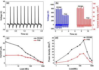
To further confirm the superior properties of PEO as the positive tribo-material for TENGs, a more specific and direct comparison between PEO60 and PA6 has been made. Fig. 3(a)
shows the VOC performance of a TENG prepared using the PEO/PA6 material combination,
with the Ni electrode of the PEO side connected to the positive lead of the oscilloscope, while the PA6 side was grounded. The structure shows a positive voltage of ~30 V, indicating that PEO is more positive in triboelectric series than that of PA6. Fig. 3(b) shows the comparison
of the VOC and JSC between the TENGs prepared with PDMS membranes in combination with
PEO60 and PA6 films respectively. For both the cases, PDMS films were used as the negative tribo-material, and tested at the same condition of 50 N force, 5 Hz frequency and 4 mm
mAm-2) of the PEO60/PDMS TENG are significantly greater than those of the PA6/PDMS
TENG (630 V, 30 mAm-2). The significantly higher output of the PEO/PDMS TENG can thus
be attributed to the higher positive electron polarity of the PEO material, and is further confirmed using the KPFM measurements as discussed later. The output powers of the PEO60/PDMS and PA6/PDMS TENGs were measured under different load resistances (R)
with the instantaneous peak power calculated as P=I2R. While the peak current of the
PEO60/PDMS TENG is much higher than that of the PA6/PDMS TENG, as shown in Fig. 3(c), with the increase in the load resistance, the value of the peak current drops off quite
rapidly. In fact, the instantaneous peak power density (Fig. 3(d)) reaches a value of 40 Wm-2
and 18 Wm-2 for the PEO60 and PA6 TENGs, respectively, both at a load resistance of about
200 MΩ. It is worth emphasizing that this reported value of ~40 Wm-2
is one of the best reported values for TENGs assembled using flat surface polymeric films. In fact, the value is
approximately three orders of magnitude (10 mWm-2) higher than that of the silk/PET TENG
[34], about ten times higher than that (5 Wm-2) of the CNTs/PDMS TENG [35], and even
higher than that (35.6 Wm-2) of the Al/PDMS TENG with nanostructured surface [16],
demonstrating the superior performance of the PEO/PDMS TENGs. It should be mentioned that the PA6 membranes prepared using the phase inversion process contains a high density of pores as compared to those of dense films formed by casting and spin-coating processes, which produces significantly higher power outputs when is utilized in TENGs [37].
Based on the above results, in order to systematically assess the performance of PEO/PDMS
TENGs, the electrical output of the PEO/PDMS (110 μm thick PEO60 film) TENG was
studied, including the VOC and JSC, under varying impact forces, impact frequencies and
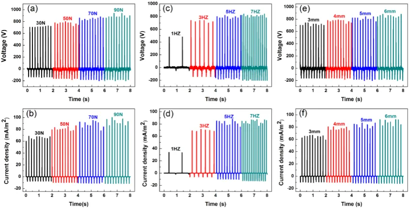
spacer distances. Figs. 4(a) and (b) show the VOC and JSC of the PEO60/PDMS TENG at
various contact forces of 30-90 N at a fixed driving frequency of 5 Hz and 4 mm spacer
distance. It can be clearly observed that the VOC increases steadily from 850 V (at 30 N) to
1070 V (at 70 N), and then slowly goes up to 1120 V (at 90 N force). The corresponding
current density shows a similar trend with the increase of force, and rises from 70 mAm-2 to
100 mAm-2 as the contact force increases from 30 to 90 N. This observed increase in the
force, which enhances the effective contact areas, thereby producing higher surface charge density and output power. The short circuit transferred charge density is one of the most important parameters for comparing the output of TENGs, and is calculated by integrating one cycle of short-circuit current pulse over time. At 50 N contact force, the charge density of
the PEO60/PDMS TENG is 154 μCm-2which further increases to 170 μCm-2 at a force of 90
N. From all the aforementioned values, it can be seen that as the contact force reaches a certain value (~80-90 N in this case), the increase in the contact area tends to saturate and the rise of voltage, current and transferred charge slowdown consequentially.
Figs. 4(c) and (d) show the VOC and JSC characteristics of the PEO60/PDMS TENG as a
function of contact frequency at a working condition of 50 N contact force and 4 mm spacer
distance. It can be clearly observed that both VOC and JSC show a similar trend wherein the
values increases rapidly with working frequency from 1-5 Hz and saturates at higher impact
frequency. In fact, the peak-to-peak VOC increases from 530 to 1020 V when the frequency
increases from 1 to 5 Hz, while the corresponding current density increases from 35 to 88
mAm-2. Such trend of electrical output can be attributed to increased contact speed under
higher frequency, leading to a faster transferring of electrons, hence higher current density and power outputs [37].
The effect of spacer distance on the VOC and JSC output of the PEO60/PDMS TENG was also
studied at a fixed 50 N contact force and 5 Hz contact frequency as shown in Figs. 4(e) and
(f). As the spacer distance is increased from 3 mm to 6 mm, the peak-to-peak VOC rises from
920 V to 1090 V, and the corresponding current density increases from 67 mAm-2 to 92
mAm-2. According to the previous work by Niu et al. [41], the VOC of the contact-mode
TENG increases with the increment of the spacer distance (x) and the inner surface charge
density (σ) via the relationship𝑉𝑂𝐶 = (𝜎.𝑥)/𝜀𝑜. Moreover, at a fixed frequency, the larger
spacer distance means a higher relative contact velocity of the PEO60 and PDMS films, which leads to a faster flow of electrons through the external circuit, thereby producing higher current density [36].
positive tribo-material is a general material property rather than specific to the PDMS. To
maintain parity with the testing conditions, the TENG contact area was kept at 2 × 2 cm2, and
tested under the same conditions as those for the PEO/PDMS TENGs: 50 N force, 5 Hz and 4
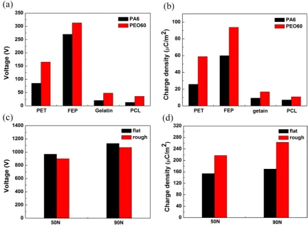
mm spacer distance. Fig. 5(a) shows the comparison of the peak-to-peak VOC for various
assembled TENGs utilizing PEO60 and PA6 as the positive tribo-materials in combination with different negative tribo-materials (PET, FEP, PCL, Gelatin), respectively. It can be seen that for all of these negative tribo-materials, TENGs with PEO60 always shows higher performance than those with PA6 membrane. Accordingly, the charge density shows the same trend wherein the PEO60 film based TENGs show higher charge density, as shown in Fig. 5(b), thus proving the suitability of PEO against not only PDMS but also other negative tribo-materials.
As triboelectrification is a surface charging effect, the surface charge density of TENGs is
expected to improve via surface treatment and nanostructuring. In order to demonstrate how
surface modification and structuring can potentially improve the output performance of PEO60/PDMS TENGs, a facile method was adopted. The method involved spin coating of PEO60 and PDMS films on sand papers (P1200, MATADOR Co.) using the same conditions as that for the synthesis of flat surface films, then peeling them off from the sand papers and gluing to the conductive adhesive Ni electrodes, with the patterned side as the contact surfaces. Surface SEM images of the PDMS and PEO films with flat and rough surfaces are shown in Fig. S1 (Supporting Information). We produced this surface structured PEO60/PDMS TENGs and tested at 4 mm spacer and 5 Hz frequency at two contact forces
(50 N, 90 N). For peak-to-peak VOC, as compared to the TENGs comprising of flat surface
films (970 V at 50 N and 1130 V at 90 N), the rough-surfaced TENGs showed a slight decrease in outputs (900 V at 50 N and 1070 V at 90 N), as shown in Fig. 5(c). However, for the rough-surfaced TENGs, the measured charge density showed significantly higher values
of 217 μCm-2 at 50 N and 263 μCm-2 at 90 N, respectively, as compared to the flat-surfaced
TENGs which displayed values of 154 μCm-2 under 50 N and 170 μCm-2 under 90 N, as
surface has a slightly higher peak-to-peak VOC than that of TENG with rough surfaces even it
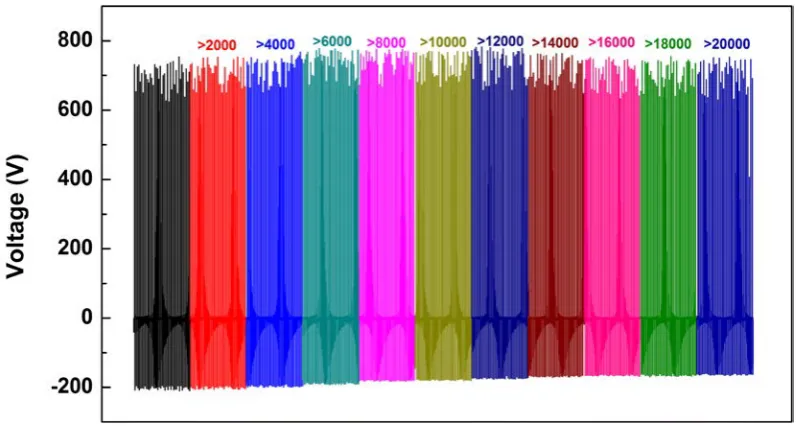
has much lower charge density. The reason is probably as follows. Since PDMS is soft with high viscosity, when the flat surface PDMS film contacts the flat surface PEO film, and they adhere very well. A relatively stronger force is needed to separate them, resulting in a faster instantaneous velocity of separation as compared to the rough surface case. This means a faster charge transferring speed through external circuit. According to the definition of current (I=dQ/dt) and voltage (V=IR, the voltage meter in our experiment is similar to a load resistance), the faster charge transferring speed can lead to a greater current and voltage value. Although the peak voltage decreases slightly for the rough-surfaced TENG, it should be noted that the total transferred charge increases significantly, so the roughness of the TENG surface leads to an improvement in the electrical performance of the PEO-based TENGs. To assess the stability of the PEO based TENGs for self-powered systems, we operated the
PEO60/PDMS TENG for over 20,000 cycles at a 5 Hz frequency for which the VOC output is
shown in Fig. 6. Within the 20,000 cyclic tests, no large deterioration of VOC was observed,
indicating that the PEO60/PDMS TENGs have excellent stability and reliability.
3.2. Mechanism for high performance TENGs with PEO film
For a contact-separation mode TENG, when the surfaces of two triboelectric materials (i.e.
PEO and PDMS) are in contact under the influence of an external mechanical force, opposite
triboelectric charges i.e. negative charges on the PDMS and positive charges on the PEO
is amply clear from the results shown above that as compared to PA6, the PEO shows a significantly higher positive tribo-effect. Let us now discuss the possible reasons for this behavior. To understand why the positive tribo-polarity of PEO polymer is greater than PA6, we characterized the surface potential between the PA6 and PEO with different molecular weights using KPFM [43].
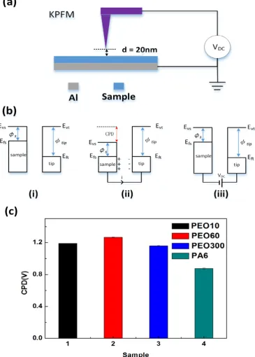
According to the working principle of KPFM, the surface potential of a sample can be
visualized as a voltage (VCPD) applied between the tip and sample to nullify the contact
potential difference (CPD), as schematically shown in Fig. 7(a). The work function of the
sample, φsample, is defined as:
𝜑𝑠𝑎𝑚𝑝𝑙𝑒 = 𝜑𝑡𝑖𝑝 − 𝑒𝑉𝐶𝑃𝐷 (1)
where φtip is the work function of the tip, VCPD is the measured contact potential difference
(CPD) between the tip and the sample, and e is the electronic charge. Firstly, the energy
levels of the tip and sample surface are presented in Fig. 7(b) <i>, with the aligned vacuum and different Fermi energy levels. Upon bringing the tip closer to the sample surface, the tip and sample surface come into electrical contact, causing the Fermi levels of the tip and sample to be aligned and thus reaching a steady-state equilibrium (as shown in Fig. 7(b) <ii>).
An external VDC is applied to the tip to nullify the electrical force, which has the same
magnitude with the developed CPD, as shown in Fig. 7(b) <iii>. The amount of applied
external bias VDC that nullifies the electrical force due to the VCPD is equal to the work
function difference between the tip and sample. Therefore, it can be seen from Equation 1
that a higher VCPD value represents a lower sample work function and it is known that for two
materials with work functions of φ1 and φ2, ifφ1 > φ2, then the φ1 material will charge
negative against the φ2 material [44], while the material with φ2 has a higher tendency to
1.160 V for PEO10, PEO60 and PEO300, respectively. It can be seen that the molecular weight has only a limited effect on the surface potential, yet the PEO60 film shows a slightly
higher CPD value than other two PEO films. As compared with PA6, a higher VCPD value for
the PEO means that PEO is more triboelectric positive, thus having a higher ability to donate electrons, and explains why the PEO/PDMS TENGs have higher outputs than that of PA6/PDMS TENGs. The detailed CPD images obtained by KPFM for the PA6, PEO10, PEO60, PEO300 films can be found in Fig. S2.
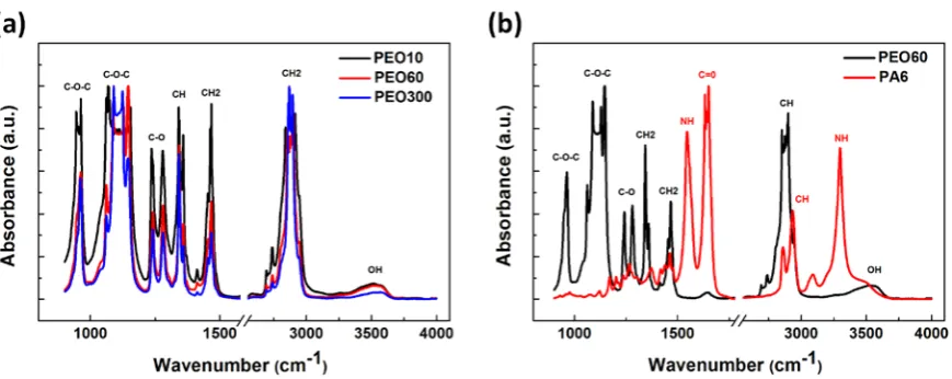
Since the surface potential of an organic material is mainly determined by its functional groups on its surface [45], FTIR measurements were conducted to investigate the functional
groups on the PA6 and PEO films (see Fig. 8(a)). The peaks at 1340 and 1466 cm-1 originate
from the vibrations of the CH2 group. The strong band from 920 to 1200 cm-1 from PEO is
attributed to the C-O-C bonds, that around 2880 cm-1 corresponds to the symmetric and
asymmetric CH stretching, while that at 3560 cm-1 is from the OH group. It can be obviously
seen that there is no significant difference between the PEO films with different molecular weights in the FTIR spectra, confirming that they have similar functional groups. This can explain the similar surface potential and triboelectric polarity for PEO10, PEO60, PEO300, and similar performance of TENGs with those PEO films. As for the PA6, the peaks are
observed at 1545 and 3300 cm-1, corresponding to the NH group, as shown in Fig. 8(b). The
peak at around 1640 cm-1 is from the ketone group, and is the most prominent, while that
around 2920 cm-1 belongs to the CH group but shows a smaller intensity than that for the
PEO films. By looking at any of the published triboelectric series of materials in the literature,
it can be observed that the nitrogen containing polymers, i.e. polymers with pyridine, amine
triboelectric series for the PEO material [47].
3.3. Applications of the PEO/PDMS TENGs
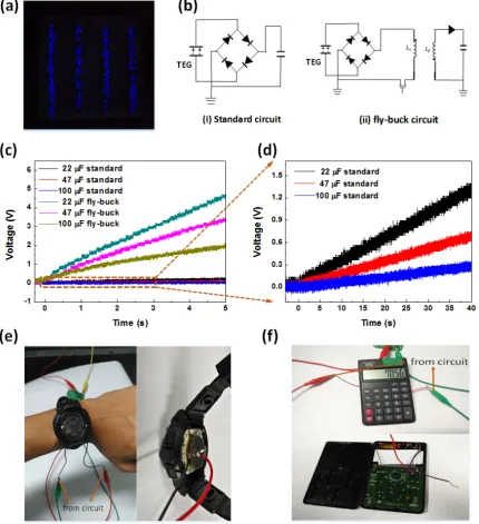
The instantaneous power being delivered by the PEO/PDMS TENGs has been exploited for
applications to power electronic devices. A 2 × 2 cm2 PEO60/PDMS TENG was found to be
able to directly light up hundreds of LEDs without any charge storage circuit as shown in Fig.
9(a) and in Supplementary video 1. For many applications, the pulsed AC nature of output
current from TENGs at a large voltage is not very useful owing to the requirements of a constant DC current with low voltage amplitude for most cases. To overcome this, a standard charge circuit is typically used to store the charges produced by a TENG (Fig. 9(b) <i>) in a
capacitor or a battery via a full-wave rectifier which is then used to power external electronic
devices. However, this also poses a problem as the TENGs normally have very high optimal
impedance (~200 MΩ in our study) with a voltage output of several hundreds of volts and
low current density, leading to low efficiency in direct charging storage. In this work, we have adopted a fly-buck circuit to improve the storage rate of the TENG output as shown in Fig. 9(b) <ii>. The fly-buck converter itself is composed of a DB107S rectifier bridge, a BSS127 MOSFET transistor; a COTS coupled inductor with a 20:1 turn ratio, a MBRM110L Schottky diode, and a storage capacitor. The transistor is controlled by a signal nanogenerator.
Figs. 9(c) and (d) show the charging curves for 22, 47 and 100 μF capacitors, respectively, by
a standard circuit and the fly-buck circuit under 5 Hz, 50 N and 4 mm operation condition for the TENG. It is clear that the charging speed of the fly-buck circuit is much faster than the standard circuit. As the TENGs were operated at the same conditions, the fast charging means
high conversion/storage efficiency. For example, while the voltage on the 100 μF capacitor
rises from 0 V to 2 V in 5 sec using the fly-buck charging circuit, the standard circuit can
only charge up to 0.04 V, corresponding to a charging speed of 0.4 Vs-1 and 0.008 Vs-1,
respectively, i.e. the charging speed of the fly-buck convertor is 50 times of the standard
circuit! Due to the fast charging abilities of the fly-buck circuit, the TENGs can be used to
drive electronic devices in real time. We utilized a 2×2 cm2 PEO60/PDMS TENG working at
digital watch as shown in Figs. 9(e) and (f). After operating the TENG for only a few cycles, the calculator and the digital watch, whose internal coin cell batteries were removed, started to work. Even after the TENG stopped working, they can still work for times up to tens of minutes because of the energy stored in the capacitor (Supplementary video 2 and 3).
4. Conclusions
In summary, poly(ethylene oxide), for the first time has been explored for the fabrication of high-performance TENGs which as compared to the existing material of choice, polyamide-6, shows a higher positive electronic polarity. In fact, when used in conjunction with PDMS as the negative tribo-material, the flat-surfaced PEO/PDMS TENG produced a power output (40
Wm-2, at 50 N contact force) more than twice that of the PA6/PDMS TENG (18 Wm-2).
Further exploration of the material properties and structure reveals that the electrical output is affected more by the thickness of the PEO film (optimal value of 110 µm) than by its molecular weight, while increasing the surface roughness led to a significant increase in the
output charge density from 170 to 263 µCm-2 at 90 N of force. The improvement of the
performance of the PEO/PDMS TENGs is mainly attributed to the high surface potential of PEO as confirmed by higher values of contact potential difference (CPD) measured using
KPFM. The work unambiguously shows a simple, cost-effective way to improve the
performance of TENGs by using PEO as the positive tribo-material. Taking into account the
bio-compatibility and environmental-friendly nature of the PEO polymer, the PEO-based
TENGs are not just good for powering electronics, but can also have broad future prospects for implantable and biodegradable electronic devices applications.
Acknowledgements
References
[1] Z.L. Wang, J.H. Song, Science, 312 (2006) 242-246.
[2] P.K. Panda, J. Mater. Sci., 44 (2009) 5049-5062.
[3] R.M. Yu, C.F. Pan, J. Chen, G. Zhu, Z.L. Wang, Adv. Funct. Mater., 23 (2013) 5868-5874.
[4] I. Sari, T. Balkan, H. Kulah, Sens. Actuator A-Phys., 145 (2008) 405-413.
[5] S.R. Hunter, N.V. Lavrik, S. Mostafa, S. Rajic, P.G. Datskos, Review of pyroelectric thermal energy harvesting and new MEMs based resonant energy conversion techniques, in: N.K. Dhar, P.S. Wijewarnasuriya,
A. Dutta (Eds.) Energy Harvesting and Storage: Materials, Devices, and Applications Iii, Spie-Int Soc Optical
Engineering, Bellingham, 2012.
[6] F.R. Fan, Z.Q. Tian, Z.L. Wang, Nano Energy, 1 (2012) 328-334.
[7] W. Tang, T. Jiang, F.R. Fan, A.F. Yu, C. Zhang, X. Cao, Z.L. Wang, Adv. Funct. Mater., 25 (2015) 3718-3725.
[8] J. Bae, J. Lee, S. Kim, J. Ha, B.S. Lee, Y. Park, C. Choong, J.B. Kim, Z.L. Wang, H.Y. Kim, J.J. Park, U.I. Chung, Nature communications, 5 (2014) 9.
[9] Y. Yang, G. Zhu, H.L. Zhang, J. Chen, X.D. Zhong, Z.H. Lin, Y.J. Su, P. Bai, X.N. Wen, Z.L. Wang, ACS Nano, 7 (2013) 9461-9468.
[10] Z.H. Lin, G. Cheng, W.Z. Wu, K.C. Pradel, Z.L. Wang, ACS Nano, 8 (2014) 6440-6448.
[11] G. Zhu, Y.J. Su, P. Bai, J. Chen, Q.S. Jing, W.Q. Yang, Z.L. Wang, ACS Nano, 8 (2014) 6031-6037.
[12] G. Zhu, Z.H. Lin, Q.S. Jing, P. Bai, C.F. Pan, Y. Yang, Y.S. Zhou, Z.L. Wang, Nano Lett., 13 (2013)
847-853.
[13] J.K. Chen, P. Ding, R.Z. Pan, W.P. Xuan, D.P. Guo, Z. Ye, W.L. Yin, H. Jin, X.Z. Wang, S.R. Dong, J.K.
Luo, Nano Energy, 34 (2017) 442-448.
[14] G. Zhu, J. Chen, Y. Liu, P. Bai, Y.S. Zhou, Q.S. Jing, C.F. Pan, Z.L. Wang, Nano Lett., 13 (2013)
2282-2289.
[15] G. Zhu, C. Pan, W. Guo, C.-Y. Chen, Y. Zhou, R. Yu, Z.L. Wang, Nano Lett., 12 (2012) 4960-4965.
[16] S.H. Wang, L. Lin, Z.L. Wang, Nano Lett., 12 (2012) 6339-6346.
[17] S.H. Wang, Y.L. Zi, Y.S. Zhou, S.M. Li, F.R. Fan, L. Lin, Z.L. Wang, J. Mater. Chem. A, 4 (2016)
3728-3734.
736-744.
[19] X.N. Xia, J. Chen, H.Y. Guo, G.L. Liu, D.P. Wei, Y. Xi, X. Wang, C.G. Hu, Nano Res., 10 (2017) 320-330.
[20] X.M. He, H.Y. Guo, X.L. Yue, J. Gao, Y. Xia, C.G. Hu, Nanoscale, 7 (2015) 1896-1903.
[21] Z. Wang, L. Cheng, Y.B. Zheng, Y. Qin, Z.L. Wang, Nano Energy, 10 (2014) 37-43.
[22] P. Bai, G. Zhu, Y.S. Zhou, S.H. Wang, J.S. Ma, G. Zhang, Z.L. Wang, Nano Res., 7 (2014) 990-997.
[23] F.R. Fan, W. Tang, Z.L. Wang, Adv. Mater., 28 (2016) 4283-4305.
[24] H.Y. Shao, Z. Wen, P. Cheng, N. Sun, Q.Q. Shen, C.J. Zhou, M.F. Peng, Y.Q. Yang, X.K. Xie, X.H. Sun,
Nano Energy, 39 (2017) 608-615.
[25] L. Jin, W.L. Deng, Y.C. Su, Z. Xu, H. Meng, B. Wang, H.P. Zhang, B.B. Zhang, L. Zhang, X.B. Xiao, M.H.
Zhu, W.Q. Yang, Nano Energy, 38 (2017) 185-192.
[26] L. Jin, J. Chen, B.B. Zhang, W.L. Deng, L. Zhang, H.T. Zhang, X. Huang, M.H. Zhu, W.Q. Yang, Z.L.
Wang, ACS Nano, 10 (2016) 7874-7881.
[27] X.S. Zhang, M.D. Han, R.X. Wang, F.Y. Zhu, Z.H. Li, W. Wang, H.X. Zhang, Nano Lett., 13 (2013)
1168-1172.
[28] Y.B. Zheng, L. Cheng, M.M. Yuan, Z. Wang, L. Zhang, Y. Qin, T. Jing, Nanoscale, 6 (2014) 7842-7846.
[29] Y. Yang, H.L. Zhang, J. Chen, Q.S. Jing, Y.S. Zhou, X.N. Wen, Z.L. Wang, ACS Nano, 7 (2013)
7342-7351.
[30] S.M. Niu, X.F. Wang, F. Yi, Y.S. Zhou, Z.L. Wang, Nature communications, 6 (2015) 8.
[31] M.H. Yeh, H.Y. Guo, L. Lin, Z. Wen, Z.L. Li, C.G. Hu, Z.L. Wang, Adv. Funct. Mater., 26 (2016)
1054-1062.
[32] Y. Jie, N. Wang, X. Cao, Y. Xu, T. Li, X.J. Zhang, Z.L. Wang, ACS Nano, 9 (2015) 8376-8383.
[33] J. Wang, Z. Wen, Y.L. Zi, P.F. Zhou, J. Lin, H.Y. Guo, Y.L. Xu, Z.L. Wang, Adv. Funct. Mater., 26 (2016)
1070-1076.
[34] X.S. Zhang, J. Brugger, B. Kim, Nano Energy, 20 (2016) 37-47.
[35] H. Wang, M.Y. Shi, K. Zhu, Z.M. Su, X.L. Cheng, Y. Song, X.X. Chen, Z.Q. Liao, M. Zhang, H.X. Zhang,
Nanoscale, 8 (2016) 18489-18494.
[36] J.K. Chen, H.W. Guo, P. Ding, R.Z. Pan, W.B. Wang, W.P. Xuan, X.Z. Wang, H. Jin, S.R. Dong, J.K. Luo,
Nano Energy, 30 (2016) 235-241.
[38] J.H. Lee, H.B. Lee, J.D. Andrade, Prog. Polym. Sci., 20 (1995) 1043-1079.
[39] N.Y. Cui, L. Gu, Y.M. Lei, J.M. Liu, Y. Qin, X.H. Ma, Y. Hao, Z.L. Wang, ACS Nano, 10 (2016)
6131-6138.
[40] Y.G. Feng, Y.B. Zheng, G. Zhang, D.A. Wang, F. Zhou, W.M. Liu, Nano Energy, 38 (2017) 27.
[41] S.M. Niu, S.H. Wang, L. Lin, Y. Liu, Y.S. Zhou, Y.F. Hu, Z.L. Wang, Energy Environ. Sci., 6 (2013)
3576-3583.
[42] K.E. Byun, Y. Cho, M. Seol, S. Kim, S.W. Kim, H.J. Shin, S. Park, S. Hwang, ACS Appl. Mater. Interfaces,
8 (2016) 18519-18525.
[43] W. Melitz, J. Shen, A.C. Kummel, S. Lee, Surf. Sci. Rep., 66 (2011) 1-27.
[44] D.W.V. Krevelen, K.T. Nijenhuis, Properties of Polymers, Springer-Verlag1980.
[45] J.E. Huheey, J. Phys. Chem., 69 (1965) 3284-&.
[46] A.F. Diaz, R.M. Felix-Navarro, J. Electrost., 62 (2004) 277-290.
Fig. 1. Device structure, photo image and fabrication process of the TENG using PEO and PDMS films as the
positive and negative tribo-materials, respectively. (a) Schematic diagram and a photo of the fabricated device,
showing the structural design of the TENG, (b) and (c) fabrication flowchart for PDMS and PEO films,
Fig. 2. Peak-to-peak open-circuit voltage (a) and charge density (b) obtained from the TENGs assembled using
different molecular weights of PEO (Mw:10000-300000) in conjunction with PDMS. Comparison with the
PA6/PDMS TENG is also shown in the same figures. The open-circuit voltage and current density of
PEO60/PDMS TENGs with different PEO film thickness (60 μm, 95μm, 110 μm and 150 μm) are presented in
Fig. 3. (a) VOC of the TENG composed of a PEO/PA6 material combination with the PEO side connecting to the
(+), and PA6 to the (-) cable of the oscilloscope, (b) presents the specific VOC and current density comparison
between the PEO60/PDMS and PA6/PDMS TENGs, showing significantly higher performance for the
PEO60/PDMS TENG than those of the PA6/PDMS TENG. (c) shows the short-circuit current and (d) the
instantaneous peak power density of the PEO60/PDMS and PA6/PDMS TENGs as a function of electrical load.
Fig. 4. Performance of the PEO60/PDMS TENG (with a 110 μm thickness PEO60 film), the open-circuit
voltage (a) and current density (b) of the TENG under different contact forces, showing the similar increasing
trend of outputs; influence of the contact frequency on the open-circuit voltage (c) and the current density (d),
which increases when values of impact frequency is less than 5 Hz and saturates beyond that; the open-circuit
voltage (e) and current density (f) with different spacer distances,again showing an increase with the increase of
Fig 5. Output performance of TENGs assembled using various negative tribo-materials with PA6 and PEO60
films as the positive tribo-materials, respectively. The obtained peak-to-peak open-circuit voltage (a) and charge
density (b) of the TENGs with PET, FEP, gelatin and PCl as the negative materials, respectively, clearly shows
the higher positive electronic affinity for PEO; (c) the variation of peak-to-peak VOC and (d) charge density of
Fig. 6. Stability of a PEO60/PDMS TENG for more than 20000 energy generation cycles at a working
Fig. 7. Working principle and measurement result of KPFM characterization on the sample surface potential. (a)
experimental setup of the KPFM; (b) working principle of the KPFM. An applied voltage on the tip is used to
eliminate the potential difference; (c) the CPD histogram of KPFM measurement for PEO films with different
Fig. 8. FTIR measurement results for different molecular weights of PEO and PA6 polymers. Comparison of
Fig. 9. Applications for a 2 ×2 cm2 PEO60/PDMS TENG. (a) Hundreds of LEDs were directly powered by a TENG without any storage capacitor; (b) schematic diagram of the standard and fly-buck charging circuits for
TENGs; (c) the comparative charge curves for 22 μF, 47 μF, 100 μF capacitors via the standard and fly-buck
charging circuits using a PEO60/PDMS TENG are shown, wherein the fly-buck circuit shows a much faster
charge speed; (d) an expanded view of the charge curves using the standard charging circuit shown in (b); and