IJE TRANSACTIONS C: Aspects Vol. 30, No. 6, (June 2017) 830-838
Please cite this article as: A. H. MogheyseandH. Miar Naimi,Effective Design of a 3×4 Two Dimensional Distributed Amplifier Based on Gate Line Considerations, International Journal of Engineering (IJE), TRANSACTIONS C: Aspects Vol. 30, No. 6, (June 2017) 830-838
International Journal of Engineering
J o u r n a l H o m e p a g e : w w w . i j e . i rEffective Design of a 3×4 Two Dimensional Distributed Amplifier Based on Gate
Line Considerations
A. H. Mogheyse*, H. Miar Naimi
Department of Electrical and Computer Engineering, Babol Noshirvani University of Technology, Babol, Iran
P A P E R I N F O
Paper history: Received 17 March 2016
Received in revised form 09 April 2017 Accepted 21 April 2017
Keywords:
Distributed Amplifier
Two Dimensional Distributed Amplifier Electrical Funnel
Power Combining
A B S T R A C T
In this paper two dimensional wave propagation is used for power combining in drain nodes of a distributed amplifier (DA). The proposed two dimensional DA uses an electrical funnel to add the currents of drain nodes. The proposed structure is modified due to gate lines considerations. Total gain improvement is achieved by engineering the characteristic impedance of gate lines and also make appropriate variation in the output of gain cells. All variations are done with respect to input and output reflection loss considerations. Analytical expression for the gain of the proposed DA is presented and design considerations for electrical funnel are discussed. Based on two dimensional power combining a wide band DA is simulated using TSMC 0.18 CMOS model in ADS which consumes 49.42 mw from 1.2V power supply. Good agreement between the proposed DA gain and calculated value is achieved. Although one stage DA is used, the final results yield a high figure of merit (FOM) in 0.18 CMOS technology. The final design shows 11.1 dB gain from near DC to 23.6 GHz, noise figure between 3 to 5.2dB and maximum output power of 7.1dBm at 1-dB output compression point (OP1dB).
doi: 10.5829/ije.2017.30.06c.02
1. INTRODUCTION1
Wideband amplifiers operating in high frequency ranges are of great interest for various applications like high speed links, high resolution radars, imaging systems, multi-mode transceivers, broadband transceivers and instrumentation systems. To achieve a broad band amplification, distributed amplifiers were first introduced in reference [1]. The idea was to absorb parasitic capacitances of transistors into transmission lines.
To enhance the characteristics of distributed amplifiers, self-equalized technique [2], matrix DA [3], gate–drain transformer feedback technique [4], tapered drain line technique [5], loss compensation technique [6, 7], cascaded multi-stage distributed amplifier (CMSDA) [8], DA with active termination [9], DA with RC gate terminal network [10], cascaded single-stage distributed amplifier (CSSDA) [11], Conventional DA (CDA)-CSSDA-CDA configuration [12], DA with
*Corresponding Author’s Email: [email protected] (A. H. Mogheyse)
Internal feedback [13] and DA with cascaded gain stages [14] have been presented since now.
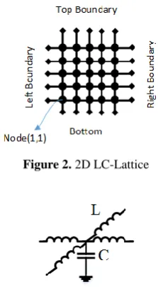
One dimensional (1D) wave propagation is used in all above techniques. Figure 1 shows some of these configurations which are always limited to 1D transmission line properties for power combining. Figure 2 shows two dimensional (2D) LC-Lattice which supports 2D wave propagation. In this figure each line represents an inductor, and each dot represents a capacitor to ground.
2D LC-Lattice has been studied before. In reference [15] for wideband signal shaping and combining, in literature [16] for ultra-fast Fourier transformer, in reference [17] for harmonic generation, in reference [18] for harmonic generation and efficient combining, in [19] for high quality factor filter and in [20] for high speed quantizer.
Electrical funnel has been used in reference [22] in drain nodes and a new structure for distributed amplification was introduced for the first time. The structure used two dimensional wave propagation. Delay time engineering and gate lines with lower impedances were used in reference [22] to achieve a better design.
In this paper another design technique is presented which helps to enhance the gain of two dimensional distributed amplifiers (2D-DA). The new technique is based on reasonable variation in the characteristic impedance of gate lines and also using output transistors proportional to the calculated output capacitance. Hence, larger widths are achieved for input and output transistors which yield a higher gain against the constant one.
The new technique and the other previous ones are used to achieve a high performance two dimensional distributed amplifier (2D-DA). Final results are extracted from one stage amplifier simulations. They lead to a high FOM which show the effectiveness of the presented techniques and 2D-DA structure.
The remainder of this paper is organized as follows. Section 2 reviews electrical funnel. In section 3 the proposed structure is introduced and all design techniques, especially the new one, are discussed. Due to the new technique, gain calculations for the proposed structure are presented in section 4. In section 5 simulation results are presented and parasitic effects are discussed. Finally, section 6 concludes this paper.
2. 2D-LC LATTICE AND ELECTRICAL FUNNEL
A unit cell of 2D LC-lattice is shown in Figure 3. By connecting number of unit cells a circuit like Figure 2 is achieved which is a 2D LC-lattice. In this figure each line represents an inductor and each node is a capacitor to ground. By this structure waves can propagate in two dimensions and we call it “lattice” for the rest of this paper.
For a straight forward propagation the characteristic impedance (Z), cutoff frequency (fcut-off) and delay per
section (T) of each node in a lattice are defined in literature [15]:
( , ) ,
( , )
1 ,
( , ) ( , )
T , ( , ) ( , )
cut off
L x y Z x y
C x y
f x y
L x y C x y
x y L x y C x y
(1)
in which L(x,y) and C(x,y) are the values of inductance and capacitance in xy-th unit cell. Electrical funnel is constructed by engineering the straight forward characteristic impedance along the wave propagation path. Assume a lattice with a characteristic impedance
like Figure 4 and a constant delay per section in all nodes. The lattice is terminated to matched loads in right and left boundaries and is opened in top and bottom boundaries. Assume that the electrical funnel is stimulated by in- phase and equal current sources (Figure 5).
Figure 1.a CDA, b CSSDA, c Matrix DA, DC biases are not shown
Figure 2. 2D LC-Lattice
A. H. MogheyseandH. Miar Naimi / IJE TRANSACTIONS C: Aspects Vol. 30, No. 6, (June 2017) 830-838 832
In this structure, current waves see parallel paths and they are guided to lower impedance paths (middle path). Each straight path from left to right is parallel to the neighbors and voltages for parallel nodes are equal. Equal voltage amplitude in vertical columns and gathering currents leads to power combining in the middle path. In this paper electrical funnel is a part of the DA. This differs from combining output power of several amplifiers by a power combiner.
3. PROPOSED STRUCTURE
Figure 6 shows the proposed two dimensional distributed amplifier (2D-DA) which is constructed by three transmission lines in the gate section and an electrical funnel for power combining in the drain section.
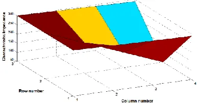
Figure 4. Characteristic impedance of a 3×4 electrical funnel
Figure 5. A 2D LC-Lattice
Inductors in the lattice and gate lines are not shown separately. Twelve gain stages are used in the structure which are arranged in three rows and four columns.
In this 2D-DA, gate artificial transmission lines are formed by inductors and gate capacitances and the drain lattice is constructed by inductors and drain capacitances. As illustrated in Figure 6, the input signal stimulates three parallel gate lines and the output power is delivered to the load at the end of electrical funnel middle path.
In this design, right and left boundaries of the drain lattice and all gate lines are terminated to match resistive loads. Terminating top and bottom boundaries of the drain lattice leads to power dissipation along the wave propagation path which is not desired.
For the best input matching, the characteristic impedances of the three parallel gate lines should be three times larger than the characteristic impedance of the input line.
To have a larger characteristic impedance while keeping cut-off frequency constant, it is necessary to have smaller capacitances in gate lines. This is due to the relations of characteristic impedance and cut-off frequency of a transmission line.
According to the straight relation between trans-conductance of each gain cell and input capacitance of gain cells, using gain cells with smaller capacitances leads to gain reduction.
A reduction in noise figure is also achievable by smaller characteristic impedance for gate lines due to lower gate line termination resistance. Furthermore, with increasing transistor widths a higher output power can be achieved.
For a distributed amplifier |S11|<-10dB is acceptable. One can easily write:
0 11
0
g sensed InputLine
g sensed InputLine
Z Z
S
Z Z
(2)
In which ZInputLine is the input line impedance, S11 is the
input reflection coefficient and Z0g-sensed is the sensed
characteristic impedance from the input of the structure.
For ZInputLine=50Ω, three parallel gate lines with 80Ω
characteristic impedance yield Z0g-sensed=26.7Ω which
can satisfy the input matching condition.
Inductors are short circuits in low frequencies, Hence in low frequencies, the equivalent of three terminating resistors of gate lines are sensed from input. But in high frequencies the square root of L/C is sensed from the first column of gate lines. The main idea of this paper is to reduce the characteristic impedance of the middle gate line from 80Ω to 50 Ω which yields larger transistors in middle path. This increases the gain of 2D-DA. A 50Ω resistor is used for termination of middle gate line. To have a reasonable input reflection loss in low frequencies, a 115Ω resistor is used for termination of top and bottom gate lines.This leads to sense 26.7Ω impedance in the input of the structure for all frequencies (Z0g-sensed=26.7Ω). Hence, Equation (2) is
satisfied for all frequencies. The characteristic impedance of each node in gate lines, Zg(x,y), is shown
in Figure 7.Zg(x,y) has been obtained by:
-3 x-2Z (x,y)=80-10g y-1 e (3)
In the proposed 2D-DA, gate lines are stimulated from left. Therefore, gain cells in a vertical column are stimulated in phase. Neglecting loss, all gain cells are assumed to be stimulated with equal voltage amplitude.
Electrical funnel is made by appropriate variation in inductors and sufficient design of gain cells. Each gain cell is designed in such a way that it achieves the desired capacitance from the output node.
The characteristic impedance in each unit cell of the proposed electrical funnel is shown in Figure 4. These values are achieved by Equation (4). In this equation, x and y represent the row and column numbers of the drain lattice and Zd(x,y) represents the value of L C/ in
each unit cell.
-3 x-2Z (x,y)=300-83.33d y-1e (4)
The right boundary of the middle path has been designed for 50Ω load.
Figure 7. Characteristic impedances of gate lines
Termination resistances for the proposed structure and reasonable bypass capacitances for a good low frequency response are listed in Table 1.
In Figure 8 two current sources with equal column number are shown. In the proposed structure, gate lines are stimulated in phase. Therefore, these two sources are in phase. If all paths have a constant delay time, due to longer path between B and G nodes in comparison with A and G nodes, signal A and B do not arrive simultaneously to G and effective power combining dose not occurr. As path B is 2times longer than path A, the delay time of node B can be designed equal to 1/ 2times shorter than the node A delay time. This design method leads to wide band power combining. The middle path has the longest delay time (Td). Hence,
it determines the lattice minimum cut off frequency (f
cut-off,min) and the total bandwidth. Td=10ps is considered
for the middle path of the proposed 2D-DA. Therefore,
fcut-off,min=1/(πTd)=31.83GHz is achieved for this
structure.
The lattice delay times are designed by assuming in phase stimulation in each column. Hence, for effective power combining in middle path, the delay time of the middle gate line is kept equal to the delay time of the drain middle path. Also the delay time of the other two gate lines should be kept equal to the delay time of the drain middle path.
By planning the desired characteristic impedance and delay time in each node, calculating the inductances (Ld(x,y)) and capacitances (Cd(x,y)) of the lattice is
done by:
,
, , , , ,
,
d d d
T x y
C x y L x y T x y Z x y
Z x y
(5)
For gate lines the inductances, Lg(x,y), and
capacitances, Cg(x,y), are calculated by:
( , ) , ( , ) ,
,
d
g g d g
g
T
C x y L x y T Z x y
Z x y
(6)
TABLE 1. Termination resistances values
Rleft R2 RGate1 RGate2 C bypass
300 Ω 300 Ω 115 Ω 50 Ω 25 pF
A. H. MogheyseandH. Miar Naimi / IJE TRANSACTIONS C: Aspects Vol. 30, No. 6, (June 2017) 830-838 834
The inductance and capacitance of each node (unit cell of the lattice) is calculated by Equation (5) and the desired lattice is achieved by inserting the equivalent values of two series inductors between two adjacent nodes. Figure 9 shows the proposed 2D-DA inductance and capacitance values.
Each gain cell has been designed to have input and output capacitances equal to the calculated values. Figure 10 shows the structure of the gain cells. As discussed in [14], due to input–output isolation, stability and bandwidth considerations and gain cells are implemented like Figure 10.
Figure 9. Calculated values for the proposed DA
Figure 10. The schematic of gain cells
In this gain cell, Li is an inductor which is used to
enhance the bandwidth. Choosing an appropriate value for Li is important to enhance the total bandwidth.
Figure 9 shows that the gain cells of the top and bottom rows should have equal input capacitances and equal output capacitances. It also shows that the input and output capacitances of gain cells vary through middle path. A 2pF capacitor is used to bypass the gates of devices. Common gate stages are biased separately through high-resistivity resistors according to stability consideration.
All parameters of Gain cells (Li, transistors widths and
necessary DC bias values in accordance with Figure 6 and Figure 10) are tabulated in Table 2. These values lead to equal trans-conductances for top and bottom rows and different trans-conductances for middle path. All trans-conductances of the proposed structure are also listed in Table 2. The trans-conductance of each gain cell in low frequencies can be calculated simply by basic relations [23].
TABLE 2. Gain cells parameters and DC bias values
Bias Conditions For All Gain Cells
VDC_gate1=0.8 V VDC_gate2=1.38 V
VDC-drain=1.2 V
For All transistors in this design
Length: 0.18 µm Unit gate width: 2 µm
Gain Cells [1-4] & [9-12]
M2 M1 Li gm
Fingers: 21 Fingers: 19 390 pH 14.45 mmho
Gain Cell [5]
M2 M1 Li gm
Fingers: 25 Fingers: 19 495 pH 14.58 mmho
Gain Cell [6]
M2 M1 Li gm
Fingers: 29 Fingers: 22 750 pH 17.1 mmho
Gain Cell [7]
M2 M1 Li gm
Fingers: 38 Fingers: 26 810 pH 21.19 mmho
Gain Cell [8]
M2 M1 Li gm
4. GAIN CALCULATION
Figure 1(a) shows CDA with N gain cells. The gate and the drain lines of the CDA are terminated in matched impedance.
Assume that gate and drain lines are matched in phase for effective power combining and have equal propagation constant. By stimulating the gate line from left boundary one can easily write the drain current of k-th transistor:
1 2 ,
j k
d k m in
I g V e
(7) in which, in
V is the amplitude of input voltage, gm is the
trans-conductance of each transistor which is assumed to be equal for all transistors and β is the phase shift per section along the propagating path. Fifty percent of drain currents flows to the load. Total output current is derived by adding all output currents:
1 2 , 1 1 2 2
N j N k
out d k m in
k
N
I I e g V
(8)Hence voltage gain (AV) and power gain (GP) are
calculated by:
0
0 2
out out d
V m d
in in
V I Z N
A g Z
V V
(9)
2
0 2 2
0 0
0 4
g
P V m d g d
Z N
G A g Z Z
Z
(10)
in which Z0g and Z0d are characteristic impedances of
the gate and the drain lines, respectively.
In the proposed structure, input signal stimulates the gate lines from the left boundary. By neglecting the loss, one can easily write the drain current of lk-th transistor:
1 2
, ,
j k
d lk m lk in
I g V e
(11)
in which l and k represent the row and column numbers. β is the phase shift per section along the wave propagation path in the gate lines and the drain lattice. In Equation (11), gm,lk is the trans-conductance of the
lk-th transistor.
In the proposed structure each incident current to the drain lattice first senses two paths. One path is to the left and the other is to the right. The current is divided between these two paths inverse proportional to the sensed resistances.
In Figure 8, the right travelling part of the drain current is calculated by Cdivision1 coefficient which is:
1
1 2
3
3 || 2
left division
left R C
R R R
(12)
in which R1=ZLoad is the load impedance and Rleft & R2
are terminating resistances (Figure 6). The right travelling current is then divided again between right boundary resistors. The load current part can be shown by Cdivision2 coefficient:
2 2 2 1 2 2 division R C R R (13)
Hence the load current by stimulating lk-th transistor, is calculated by:
2 2
1 2
1
( 1) 2 1 2 2
,
load lk division division
j k j M l N k
m lk in
I C C
g V e e
(14)
in which
2 2
(M1) 2l N k 1 2 represents the phase shift from lk-th node of the drain lattice to the load. M and N are the numbers of rows and columns which are 3 and 4 in this design. By adding all drain currents, total load current is achieved by:
2 2
1 2
1
( 1) 2 1 2 2
, 1 1
load division division in
M N j k j M k N l
m lk l k
I C C V
g e e
(15)and the power gain is calculated by:
2 2
2
2
0 2
1 2 0
2 1
( 1) 2 1 2
2 , 1 1 1 2 1 2 load load P in g sensed
division division load g sensed
M N j k j M l N k m lk l k Z I G V Z
C C Z Z
g e e
(16)Designing the drain lattice in such a way that all drain currents can arrive in-phase, the power gain is calculated by:
2
1 2 , 0
1 1
M N
P division division m lk load g sensed l k
G C C g Z Z
(17)5. SIMULATION RESULTS
For the proposed 2D-DA, in-phase additive gain mechanism has been used. Hence, the gain can be calculated by Equation (17). According to the designed input impedance, M=3&N=4 and Table 2, one can easily calculate the power gain GP=15 which yields
|S21|=11.76 dB. This value has been achieved by
neglecting the loss of inductors.
A. H. MogheyseandH. Miar Naimi / IJE TRANSACTIONS C: Aspects Vol. 30, No. 6, (June 2017) 830-838 836
the total bandwidth. However, there is another limiting factor in an optimized design. Taking limited self-resonant frequency (SRF) of inductors into account, it should be noted that in this wide bandwidth structure and with today’s inductor implementation methods, we are restricted to self-resonance property of inductors instead of the total cutoff frequency.
The maximum value of inductors in the proposed structure is 2.68nH. A 2.68nH inductor has been simulated by ADS electromagnetic (EM) simulator with TSMC 0.18 CMOS layout specifications. Simulation shows that the SRF of inductors is a problem in the proposed structure.
To solve the problem, some simulations in schematic level are made. These simulations show that if all inductors of the drain lattice are restricted to 1.5 nH, the bandwidth of the proposed circuit does not change seriously and it just dictates a little reasonable ripple in pass band. It is not desired but it helps to make the circuit implementable. It is shown that the total performance of the circuit covers this problem perfectly.
Other aspects of layout implementations are discussed in [22]. Especially the effect of connections in the sensed inductance between two nodes should be considered.
The proposed circuit has been simulated by ADS with TSMC 0.18 CMOS model. Using inductors with Q=14 at 5 GHz degrades the gain.
Figure 11 shows the results of four simulations. The proposed 2D-DA with the discussed change in the value of inductances is the first simulation. The second one is the simulation of the proposed 2D-DA with no change in the values of inductances. As Figure 11 shows, just a little ripple has been dictated to the passband.
According to the results of the first simulation, the proposed circuit shows 11.1 dB gain. There is a good agreement between calculated values and simulation results. Simulation shows 23.6 GHz bandwidth which yields 84.71 GHz gain bandwidth. The amplifier consumes 41.18 mA from 1.2 V DC source which yields 49.42 mw DC power consumption.
The other two simulations are done to show how the proposed technique can improve the performance of DAs. Simulation three is done with no change in the characteristic impedance of the middle gate line. The last one is the simulation of a CDA (one dimensional conventional distributed amplifier) which uses the largest transistors of the ones in Table 2 for all gain cells. The CDA is constructed by 4 gain cells. These conditions help to make the results of CDA and final 2D-DA comparable.
It is concluded from Figure 11 that the considered techniques have improved the gain of the proposed 2D-DA while acceptable input and output reflection losses are also achieved (Figure 12). This has been achieved by the appropriate design based on Equation (2) and other discussed considerations.
Although |S12| is not perfect, the overall performance of the proposed DA is good. This structure can be cascaded with other ones or even with itself to cover this problem while other aspects like gain, NF, S11, S22
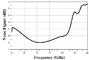
and OP1dB are constant or have a reasonable value. Figure 13 shows the NF of the proposed 2D-DA. The amplifier has a good NF which is between 3-5.2 dB across the bandwidth.
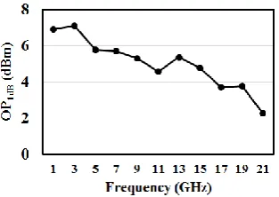
Output power in one dB compression point (OP1dB)
is shown in Figure 14. Maximum value of OP1dB is 7.1
dBm at 2GHz which is a good result.
Table 3 summarizes these work specifications against previous works. Table 3 shows that the circuit has FOM1=66 which is a comparable result against other design methods in 0.18 CMOS technology.
Figure 11. Gain of the proposed 2D-DA, (simulation 1) and three other DA’s
Figure 12. Scattering parameters of the proposed 2D-DA (from Simulation 1)
Figure 14. OP1dB of the proposed 2D-DA (with Simulation 1 conditions)
6. CONCLUSION
A new structure of 2D-DA was designed for wideband amplification. In this circuit, power combining was performed by electrical funnel. Appropriate values for gate lines characteristic impedance was chosen according to output power delivery, noise and gain considerations. Gain relation for the proposed circuit was reported and a delay time engineering method was considered to achieve broad band amplifier design. Very good agreement between simulations and relations were realized. The proposed circuit was simulated by TSMC 0.18 COMS model in ADS.
TABLE 3. Performance summary and comparison with prior works
Results
From Process
Gain (dB)
BW (GHz)
GBW (GHz)
fT
(GHz) PDC
(mw)
OP1dB
(dBm)
NF
(dB) FOM1 FOM2 Ref
FAB 0.18 µm
CMOS 20 39.4 394 50 250
6.5 @20GHz
8-9.4
<18 GHz 19 1.58 [14]
FAB 0.18 µm
CMOS 24 33 523 50 238
7.5 @5GHz
6.5-7.5
<18GHz 51 2.19 [12]
SIM 0.18 µm
CMOS 7.3 14 32.5 - 52 - 4.3-6.1 - 0.62 [2]
FAB 0.18 µm
CMOS 6 27 53.9 - 68 - 6 - 0.79 [24]
FAB 0.18 µm
CMOS 9.5 32 95.5 - 71 - - - 1.34 [4]
FAB 0.13 µm
CMOS 8.5 52 138 - 142 - - - 0.97 [25]
SIM 0.18 µm
CMOS 11.1 23.6 84.71 50 49.42
7.1
@ 2 GHz 3-5.2 66 1.71
This Work
1 ,
1 1000 dB , 2
T DC N avg DC
OP
GBW GBW
FOM FOM
f P F P
, FAB: Fabrication, SIM: Simulation
This 2D-DA shows 78.3 GBW with 49.42 mw DC power consumption. Noise figure was achieved from 3dB to 5.2dB and the maximum OP1dB was 7.1dBm.
The simulated 2D-DA shows a high FOM in 0.18 CMOS. Although the gain improvements were achieved by changing the gate line characteristic impedance, simulations show acceptable input and output reflection losses.
7. REFERENCES
1. Percival, W., "Thermionic valve circuits", British patent, Vol. 460562, No., (1937), 25-32.
2. Mohammad-Taheri, M., "Self-equalized distributed amplifier for wide band optical transceivers", International Journal of Engineering-Transactions A: Basics, Vol. 17, No. 3, (2004), 263-270.
3. Chien, J.-C., Chen, T.-Y. and Lu, L.-H., "A 9.5-db 50-ghz matrix distributed amplifier in 0.18-/spl mu/m cmos", in VLSI Circuits,. Digest of Technical Papers. Symposium on, IEEE., (2006), 146-147.
4. Hsiao, C.-Y., Su, T.-Y. and Hsu, S.S., "Cmos distributed amplifiers using gate–drain transformer feedback technique",
IEEE Transactions on Microwave Theory and Techniques, Vol. 61, No. 8, (2013), 2901-2910.
5. Sinsoontornpong, P., Roopkom, I. and Worapishet, A.,
"Cascaded high-gain distributed amplifier configuration for
enhanced gain-bandwidth product", in Electrical
Engineering/Electronics, Computer, Telecommunications and Information Technology (ECTI-CON), 10th International Conference on, IEEE., (2013), 1-5.
6. Li, Y., Goh, W.-L., Tang, H., Liu, H., Deng, X. and Xiong, Y.-Z., "A 10 to 170 ghz distributed amplifier using 130-nm sige hbts", in Integrated Circuits (ISIC), International Symposium on, IEEE., (2016), 1-4.
7. Mohammad-Taheri, M. and Elmasry, M.I., "Ultra-widband distributed amplifier using loss compensation technique on both input and output circuit", International Journal of Engineering-Transactions A: Basics, Vol. 17, No. 4, (2004), 377-383.
8. Arbabian, A. and Niknejad, A.M., "Design of a cmos tapered cascaded multistage distributed amplifier", IEEE Transactions on Microwave Theory and Techniques, Vol. 57, No. 4, (2009), 938-947.
9. Mesgari, B., Saeedi, S. and Jannesari, A., "A wideband low noise distributed amplifier with active termination", in Telecommunications (IST), 7th International Symposium on, IEEE., (2014), 170-174.
209 A. H. MogheyseandH. Miar Naimi / IJE TRANSACTIONS C: Aspects Vol. 30, No. 6, (June 2017) 830-838
terminal network for ultra-wideband pulse radio systems", IET Microwaves, Antennas & Propagation, Vol. 6, No. 2, (2012), 127-134.
11. Beheshti, I., Uysal, S., Farokhiyan, F. and Azar, F., "Design of broadband bandpass cascaded singlestage distributed amplifier in 0.13 μm cmos technology for uwb applications", in Business, Engineering and Industrial Applications (ISBEIA), IEEE Symposium on, IEEE. (2012), 33-36.
12. Chen, P., Kao, J.-C., Huang, P.-C. and Wang, H., "A novel distributed amplifier with high gain, low noise and high output power in 0.18-µm cmos technology", in Microwave Symposium Digest (MTT), IEEE MTT-S International, IEEE., (2011), 1-4. 13. Arbabian, A. and Niknejad, A.M., "A broadband distributed
amplifier with internal feedback providing 660ghz gbw in 90nm cmos", in Solid-State Circuits Conference, 2008. ISSCC 2008. Digest of Technical Papers. IEEE International, IEEE., (2008), 196-606.
14. Chien, J.-C. and Lu, L.-H., "40-gb/s high-gain distributed amplifiers with cascaded gain stages in 0.18-$\ mu {\ hbox {m}} $ cmos", IEEE Journal of Solid-State Circuits, Vol. 42, No. 12, (2007), 2715-2725.
15. Afshari, E., Bhat, H.S., Hajimiri, A. and Marsden, J.E., "Extremely wideband signal shaping using one-and two-dimensional nonuniform nonlinear transmission lines", Journal of Applied Physics, Vol. 99, No. 5, (2006), 054901.
16. Afshari, E., Bhat, H.S. and Hajimiri, A., "Ultrafast analog fourier transform using 2-d lc lattice", IEEE Transactions on Circuits and Systems I: Regular Papers, Vol. 55, No. 8, (2008), 2332-2343.
17. Lilis, G.N., Park, J., Lee, W., Li, G., Bhat, H.S. and Afshari, E., "Harmonic generation using nonlinear lc lattices", IEEE
Transactions on Microwave Theory and Techniques, Vol. 58, No. 7, (2010), 1713-1723.
18. Bhat, H.S. and Afshari, E., "Nonlinear constructive interference in electrical lattices", Physical Review E, Vol. 77, No. 6, (2008), 066602.
19. Momeni, O. and Afshari, E., "Electrical prism: A high quality factor filter for millimeter-wave and terahertz frequencies",
IEEE Transactions on Microwave Theory and Techniques, Vol. 57, No. 11, (2009), 2790-2799.
20. Tousi, Y.M. and Afshari, E., "2-d electrical interferometer: A novel high-speed quantizer", IEEE Transactions on Microwave Theory and Techniques, Vol. 58, No. 10, (2010), 2549-2561. 21. Afshari, E., Bhat, H., Li, X. and Hajimini, A., "Electrical funnel:
A broadband signal combining method", in Solid-State Circuits Conference, 2006. ISSCC 2006. Digest of Technical Papers. IEEE International, IEEE. Vol., No. Issue, (2006), 751-760. 22. Mogheyse, A.H. and MiarNaimi, H., "Two-dimensional
distributed amplifier by 2d-lc lattice", IET microwaves, antennas & propagation, Vol. 10, No. 14, (2016), 1581-1590. 23. Razavi, B. Design of Analog CMOS Integrated Circuits”, New
York: McGraw-Hill, (2001).
24. Amaya, R.E., Tarr, N. and Plett, C., "A 27 ghz fully integrated cmos distributed amplifier using coplanar waveguides", in Radio Frequency Integrated Circuits (RFIC) Symposium, 2004. Digest of Papers. 2004 IEEE, IEEE. Vol., No. Issue, (2004), 193-196. 25. Egels, M., Gaubert, J., Pannier, P. and Bourdel, S., "A 52-ghz
8.5-db traveling-wave amplifier in 0.13-$\ mu $ m standard cmos process", IEEE Transactions on Microwave Theory and Techniques, Vol. 56, No. 5, (2008), 1226-1233.
Effective Design of a 3×4 Two Dimensional Distributed Amplifier Based on Gate
Line Considerations
A. H. Mogheyse, H. Miar Naimi
Department of Electrical and Computer Engineering, Babol Noshirvani University of Technology, Babol, Iran
P A P E R I N F O
Paper history: Received 17 March 2016
Received in revised form 09 April 2017 Accepted 21 April 2017
Keywords:
Distributed Amplifier
Two Dimensional Distributed Amplifier Electrical Funnel
Power Combining
ديكچ ه
تیوقت .تسا هدش هدافتسا ،هدش عیزوت هدننک تیوقت نیرد رد ناوت بیکرت یارب جاوما یدعب ود راشتنا زا هلاقم نیا رد
کی زا رظن دروم یدعب ود هدننک
Electrical Funnel
دروم راتخاس .دنک یم هدافتسا نیرد طاقن نایرج ندرک عمج یارب
زا .دوش یم حلاصا تیگ تاظحلام هب هجوت اب رظن رد بسانم تارییغت داجیا و اه تیگ طوطخ سنادپما یسدنهم قیرط
تاظحلام هب هجوت اب هدش لامعا تارییغت یمامت .دوش یم لصاح هدننک تیوقت یلک نیگ دوبهب ،نیگ یاه لولس یجورخ
رظن دروم هدش عیزوت هدننک تیوقت نیگ یارب یلیلحت طباور .تسا هدش ماجنا یجورخ و یدورو رد ساکعنا تافلت هئارا
یحارط تاظحلام و تسا هدش
Electrical Funnel
تیوقت کی یدعب ود ناوت بیکرت ساسا رب .تسا هدش ثحب
لدم زا هدافتسا اب دناب نهپ هدش عیزوت هدننک
TSMC 0.18 CMOS
رد
ADS
اب ربارب یناوت هک تسا هدش یزاس هیبش
49.42
عبنم زا تاو یلیم
1.2
تسدب خساپ .دنک یم فرصم یتلو هب هدش عیزوت هدننک تیوقت نیگ یزاس هیبش زا هدمآ
،ییاهن جیاتن ،دراد هقبط کی اهنت رظن دروم هدش عیزوت هدننک تیوقت هکنیا اب .تسا کیدزن هدش هبساحم رادقم هب یبوخ
FOM
یژولونکت رد ییلااب
0.18 CMOS
اب ربارب ینیگ ،ییاهن حرط .دنا هداد تسدب
11.1 dB
ابیرقت زا
DC
ات
23.6
GHz
نیب رگیف زیون ،
3 dB
ات
5.2 dB
اب ربارب یجورخ ناوت نیرتشیب و
7.1 dBm
یگدرشف هطقن رد
1 dB
تسدب