© Author(s) 2017. This work is distributed under the Creative Commons Attribution 3.0 License.
Channel Analysis for a 6.4 Gb s
−
1
DDR5
Data Buffer Receiver Front-End
Stefanie Lehmann and Friedel Gerfers
Chair of Mixed Signal Circuit Design, Technische Universität Berlin, Einsteinufer 17, 10587 Berlin, Germany
Correspondence to:Stefanie Lehmann (s.lehmann@tu-berlin.de)
Received: 29 December 2016 – Revised: 28 April 2017 – Accepted: 7 May 2017 – Published: 21 September 2017
Abstract. In this contribution, the channel characteristic of the next generation DDR5-SDRAM architecture and possible approaches to overcome channel impairments are analysed.
Because modern enterprise server applications and net-works demand higher memory bandwidth, throughput and capacity, the DDR5-SDRAM specification is currently under development as a follow-up of DDR4-SDRAM technology. In this specification, the data rate is doubled to DDR5-6400 per IO as compared to the former DDR4-3200 architecture, resulting in a total per DIMM data rate of up to 409.6 Gb s−1. The single-ended multi-point-to-point CPU channel architec-ture in DDRX technology remains the same for DDR5 sys-tems. At the specified target data rate, insertion loss, reflec-tions, cross-talk as well as power supply noise become more severe and have to be considered. Using the data buffer re-ceiver front-end of a load-reduced memory module, sophisti-cated equalisation techniques can be applied to ensure target BER at the increased data rate.
In this work, the worst case CPU back-plane channel is analysed to derive requirements for receiver-side equalisa-tion from the channel response characteristics. First, chan-nel impairments such as inter-symbol-interference, reflec-tions from the multi-point channel structure, and crosstalk from neighboring lines are analysed in detail. Based on these results, different correction methods for DDR5 data buffer front-ends are discussed. An architecture with 1-tap FFE in combination with a multi-tap DFE is proposed. Simulation of the architecture using a random input data stream is used to reveal the required DFE tap filter depth to effectively elimi-nate the dominant ISI and reflection based error components.
1 Introduction
Modern server applications require a high capacity, high speed and low latency memory architecture. Using a high speed link between CPU and memory, data has to be trans-mitted at increasing data rates to the memory known as dual inline memory modules (DIMM). The IO frequencies in DDR-SDRAM show the trend to double with every tech-nology and reach up to 3.2 Gb s−1dual data rate in DDR4. Hence, DDR5-SDRAM is expected to achieve data rates as high as 6.4 Gb s−1per line. Modern CPUs support up to four channels in parallel, with 3 DIMM slots per channel being supported in DDR4, and 2 DIMM slots in DDR5. Increas-ing the memory capacity by populatIncreas-ing multiple DIMM per channel also increases the capacitive load. This decreases the channel’s bandwidth and results in lower IO frequencies. Therefore, buffered memory modules with reduced load have been developed. Depending on the application, variants of DIMMs differing in performance are available. Unbuffered DIMM is used in consumer applications with low require-ment in memory capacity and achieves high data rates in single DIMM per channel configurations. Registered DIMM (RDIMM) and load reduced DIMM (LRDIMM) are both of-ten used in server applications. There, high data rates can be maintained while populating multiple DIMM per chan-nel, resulting in increased memory capacity. A configuration for LRDIMM is depicted in Fig. 1.
oppor-RCD SDRAM DB SDRAM DB SDRAM DB SDRAM DB SDRAM DB SDRAM DB SDRAM DB SDRAM DB
CPU
M em ory c o
nt ro ll er RCD SDRAM DB SDRAM DB SDRAM DB SDRAM DB SDRAM DB SDRAM DB SDRAM DB SDRAM DB 8 224 8 8 8 8 8 8 8
Figure 1.Configuration of a DDR5 memory architecture. The CPU is connected to two LRDIMMs in parallel. The data signals are con-nected to the data buffers (DB), the clock and control signals to the register-clock-driver (RCD).
tunity to equalise the received data signals and improve the signal integrity to obtain target data rates. However, the la-tency resulting from equalisation and post processing must be kept reasonably low to avoid large memory access times. The interface between CPU and memory modules is speci-fied in an open standard provided by theJEDECorganisation to achieve inter-operability with different components. For DDR5, the standard has not yet been published. Therefore, requirements for a data buffer receiver front-end are derived from channel characteristics and from former standards such as DDR4-SDRAM (JEDEC Solid State Technology Associ-ation, 2015).
2 Channel characteristics
The channel between CPU and DIMM is a FR4 copper back-plane channel. Due to bandwidth limitations, the expected channel characteristic shows a low pass behavior. To consider the worst case scenario of a lossy channel, a model for a long back-plane channel is used for simulation and receiver front-end design, because it has the highest attenuation and is most prone to channel impairments. The frequency response of the channel is shown in Fig. 2.
In this example, the attenuation of the victim decreases to −9.8 dB at 3.2 GHz bandwidth. The response observed at the aggressors resembles the crosstalk that would be re-ceived from the respective line due to parasitic capacitive coupling1. The frequency response from the dominant ag-gressor is−18.5 dB at 3.2 GHz bandwidth.
DDR memory architecture is a single-point to multi-point channel architecture. In CPU write mode, the CPU transmits data to one of the DIMMs, referred to asactivemodule. The 1The port order does not resemble the physical routing position
of the data lines within the motherboard. Hence, crosstalk of the first and second neighboring lines is independent of port order because it depends on the wire routing on the back-plane. Therefore, a second neighbor port can have higher coupling than the direct neighbor.
Figure 2.Long channel frequency response of the backplane chan-nel between CPU and DIMM for a modern server configuration. Stimulus is applied tovictim, with two DIMMs per channel popu-lated.Aggressors are first order (dashed) and second order (dotted) neighboring ports tovictim. The targeted bandwidth of 3.2 GHz cor-responding to a data rate of 6.4 Gb s−1is marked.
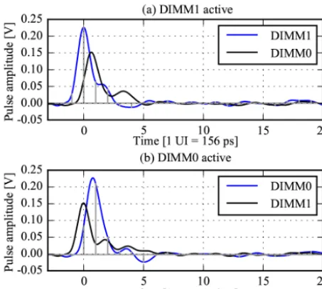
termination resistance on both modules is adjusted so that the signal amplitude received at the active module is increased. An example for a long channel impulse response is shown in Fig. 3. Due to impedance mismatch, reflections can occur at each connection point. E.g., an impulse transmitted from the memory controller is observed at DIMM1 and partially reflected at DIMM0. The reflection reoccurs at DIMM1 after the round-trip time has passed. As of Fig. 3, the round-trip time is of order 1.5 UI2.
In Fig. 3b, it can be observed that DIMM0 shows a differ-ent response pattern as compared to the DIMM1 response. Stems within Fig. 3a indicate ideal sampling points for DIMM1 and are in the following referred to as cursors, with the main cursor being located at 0. It can be seen that pre-and post cursor inter-symbol-interference (ISI) is present. It can be concluded that the channel has different forms of im-pairments that have to be considered in the receiver front-end design. Channel bandwidth limitation causes severe ISI such as pre cursor interference as well as post cursor interference. Reflections result in a long tail impulse response, interfering symbols with up to 6 unit intervals delay. The receiver eye of a random bit stream is shown in Fig. 4. Crosstalk is in-creased at target frequency and has to be canceled as well. Due to the link being single ended, also supply noise has to be considered.
3 Equalisation Methods
A selection of different equalisation methods implemented in modern wireline receivers is presented in Liu and Lin (2004). A continuous time linear equaliser (CTLE) is a com-mon method to compensate for a linear low pass behavior
Figure 3.Long channel impulse response with two DIMM popu-lated.(a)DIMM1 set active,(b)DIMM0 set active. Time scale is normalised to unit intervals (UI) with 1 UI=156 ps, corresponding to target data rate of 6.4 Gb s−1, and 0 being the ideal sampling point for the pulse at DIMM1.
0.0 0.2 0.4 0.6 0.8 1.0 Time [1 UI = 156 ps] 0.6
0.7 0.8 0.9 1.0
DB input
Y
oltage [V]
DIMM1 without xtalk
0.0 0.2 0.4 0.6 0.8 1.0 Time [1 UI = 156 ps] 0.6
0.7 0.8 0.9 1.0
DIMM1 with xtalk
Figure 4.Receiver eye of active DIMM1 with and without crosstalk and no equalisation applied. Time scale is normalised to unit inter-vals (UI) with 1 UI=156 ps, corresponding to target data rate of 6.4 Gb s−1.
of a channel by amplification of high frequencies. As can be seen in Fig. 2, the frequency response is rather complex and therefore the CTLE requires a complex high pass filter for compensation. The major drawback is that by amplifying higher frequencies, crosstalk is also amplified, which is al-ready a severe issue at the targeted frequency. Therefore, and also because of the complex compensation, a CTLE is not applicable for the equalisation in a data buffer front-end.
Feed forward equalisers (FFE) filter the input signal with a finite impulse response (FIR). Depending on the filter co-efficients, pre cursor as well as post cursor ISI can be can-celed (Agrawal et al., 2012). Cancellation of the pre cursor at
t= −1 UI involves the delay of the input signal by 1 UI. This delay adds up to the overall latency of the receiver front-end, thus the benefit of a FFE has to be compared to a possibly increased access time. The complexity of an analog multi-tap FFE does not scale linearly with the number of multi-taps and can get complex due to the required analog delay line. Be-cause post cursor cancellation requires up to 6 taps, a FFE is not sufficient for post cursor ISI cancellation. For the data buffer front-end, a FFE can be used efficiently for 1-tap pre cursor cancellation in combination with another architecture that cancels the remaining post cursor ISI, such as a decision feedback equaliser (DFE).
A DFE compensates post cursor ISI by subtracting fixed tap values from the input signal, depending on the quantised (sliced) signal of previous received symbols. The slicer out-put is a digital signal and can be delayed more efficiently than an analog signal. Therefore, multiple taps can be im-plemented to cancel post cursor ISI and also back reflec-tion from CPU, which requires compensareflec-tion after a delay of about 20 UI. As an advantage of the DFE, noise and crosstalk is not amplified. Due to its dependence on previous symbols, it can only compensate for post cursor ISI and must be com-bined with a pre cursor cancellation method such as the FFE. If the slicer decision is false due to e.g. crosstalk or noise, the applied tap sequence distorts the input signal and can lead to a propagation of the error.
The proposed architecture for a data buffer receiver front-end is shown in Fig. 5. Because crosstalk is an increasing issue at higher data rates, the use of a DFE is most beneficial as it does not amplify crosstalk. However, signal amplitudes below slicer threshold are not detected and will further prop-agate through the system. This happens e.g. for pre cursor signals, which must be equalised using a FFE.
4 Simulation
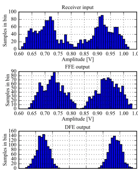
The proposed architecture in Fig. 5 with a 1-tap FFE and a multi-tap DFE is used for the equalisation of a random data stream. Concluding from channel analysis, 6 DFE taps are sufficient to cancel the most severe post cursor ISI. The chan-nel output signal is sampled in time at ideal sampling points and then filtered by the proposed architecture. The effect of crosstalk is simulated by applying random data streams to all data lines. The result is shown in Fig. 6 in the form of histograms, which resemble the receiver eye opening of the input being sampled at the specified sampling points3. It can be seen that without equalisation, the eye is closed at the re-ceiver input (top plot). Filtering with a 1-tap FFE removes the pre cursor ISI, but the eye is still fairly closed. After equali-sation by a 6-tap DFE, most of the post cursor ISI is removed and the eye is opened (bottom plot).
3The histogram can be considered as a vertical slice of the
FFE
DFE
Memory
c
ontroller
TX
Channel
z-1
z-1
a1 1
z-1
z-n+2
b2
bn
b1
D
FE
o
ut
H(s) ZOH
DB front-end
RODT,TX
VDD
RODT,RX
VDD
Figure 5.Proposed data buffer front-end architecture with 1-tap FFE and multi-tap DFE.
0.60 0.65 0.70 0.75 0.80 0.85 0.90 0.95 1.00 1.05
Amplitude [V]
0
20
40
60
80
100
Samples in bin
Receiver input
0.60 0.65 0.70 0.75 0.80 0.85 0.90 0.95 1.00 1.05
Amplitude [V]
0
10
20
30
40
50
60
70
80
90
Samples in bin
FFE
output
0.70
0.75
0.80
0.85
0.90
0.95
1.00
1.05
Amplitude [V]
0
20
40
60
80
100
120
140
160
Samples in bin
DFE
output
Figure 6.Histograms showing the distribution of voltage levels ob-tained from a data stream of 2 k samples. The respective plots show the distribution without equalisation at the receiver input (top), after FFE filtering (middle) and after DFE equalisation (bottom).
The bit error ratio (BER) is estimated by statistical eval-uation of the data (Balamurugan et al., 2009). At a target BER of 10−12, the proposed structure opens the receiver eye with 80 mV without crosstalk. However, with consideration of crosstalk, the receiver eye is closed at a BER of 10−12. Increasing the number of DFE taps does not improve perfor-mance condsidering crosstalk, therefore additional measures for crosstalk cancellation have to be taken.
5 Conclusions
In this paper, the worst case DDR5 channel characteris-tics have been analysed at the maximum target data rate of 6.4 Gb s−1. Results have shown that the LRDIMM receive signal at the data buffer input suffers from severe ISI, reflec-tions from the multi-point channel architecture, and crosstalk originating from neighbouring IOs. As an example, pre- and post cursor interference is introduced by the limited channel bandwidth.
Based on the obtained results, different correction meth-ods for DDR5 data buffer front-ends have been discussed. A 1-tap FFE architecture is demanded to cancel the pre cursor impairment on the receiver side. The drawback of the FFE is a 1 UI receiver latency. In addition to the FFE a multi-tap DFE is proposed. Channel simulations reveal a 6 tap DFE filter depth to effectively eliminate both, ISI and reflection based error components.
The proposed channel equalisation using the combination of a FFE and a DFE reliably opened the receiver eye with 80 mV @ 10−12BER excluding crosstalk. Crosstalk cancel-lation is required to open the receiver eye and obtain target BER.
Data availability. Proprietary channel model from company was
used and is not publicly available.
Competing interests. The authors declare that they have no conflict
of interest.
Edited by: J. Anders
Reviewed by: two anonymous referees
References
both 4-tap FFE and 5-tap DFE functions in 45 nm SOI CMOS, in: Proc. IEEE Int. Solid-State Circuits Conf., 19–23 February 2012, San Francisco, USA, 134–136, https://doi.org/10.1109/ISSCC.2012.6176951, 2012.
Balamurugan, G., Casper, B., Jaussi, J. E., Mansuri, M., O’Mahony, F., and Kennedy, J.: Modeling and Analysis of High-Speed I/O Links, IEEE T. Adv. Packaging, 32, 237–247, https://doi.org/10.1109/TADVP.2008.2011366, 2009.
JEDEC Solid State Technology Association: DDR4 SDRAM Load Reduced DIMM Design Specification, available at: https://www. jedec.org (last access: 24 May 2017), 2015.