Vol. 4, No. 1-2, 2015, 11-22
11
Jo
u
rn
a
l o
f
M
a
th
e
m
a
ti
c
a
l N
a
n
o
S
c
ie
n
c
e
Band gap modulation of graphyne: A density
functional theory study
ROYA MAJIDI
Department of Physics, Faculty of Science, Shahid Rajaee
Teacher Training University, Tehran, 16785 – 136, I R. Iran
Email: [email protected], [email protected]
ABSTRACT. Modifying the electronic properties of graphyne via doping, organic molecule adsorption, and chemical functionalization was reviewed. The electronic band structure and density of states were studied by using density functional theory. The α-graphyne was considered due to its analogous to graphene. The results indicate α-graphyne is a semimetal with zero band gap. It was shown that doping, adsorbing organic molecule, and chemical functionalization can open a band gap in α-graphyne. The size of the band gap was dependent on the concentration of impurity, adsorbed TCNE or CCl2 molecules. The mentioned methods
provide the possibility of opening an energy band gap in α-graphyne as required for fabricating high-performance nanoelectronic devices based on graphyne.
Keywords: α-graphyne, doping, organic molecule adsorption, functionalization, electronic properties
1. INTRODUCTION
Carbon’s hybridization states (sp, sp2, and sp3) can lead to form various carbon
allotropes such as diamond (sp3), graphite (sp2), fullerene (sp2), carbon nanotube
(sp2), and graphene (sp2) [1]. Among these carbon based nanomaterials, a two
12
Jo
u
rn
a
l
o
f
M
a
th
e
m
a
ti
c
a
l
N
a
n
o
S
c
ie
n
c
e
a single point at the Fermi level. It means graphene is a semiconductor with zero band gap known as a semimetal [1, 5]. Beyond these well known allotropes, new members named as graphyne was predicted and added to the carbon family in recent years [6, 7]. Graphyne, a single atomic layer of carbon sheet, was obtained by replacing some of carbon bonds in graphene with acetylenic linkages [7]. The resulting networks include
sp-hybridized carbon atoms together with sp2-hybridized carbon atoms. Three various
types of graphyne (α, β, γ) were built by inserting carbon triple bond into carbon single bonds in graphene. The presence of acetylenic groups in these structures introduces a rich variety of electrical, optical, and mechanical properties [6, 8]. One of the most exciting features of graphynes is related to its unusual electronic properties. It was reported that some graphynes have gapless band structure with unusual Dirac-like electronic excitations [9, 10]. It means the Dirac cone Dirac-like feature is not a unique characteristic of graphene [10] and does not depend on the hexagonal symmetry of carbon sheets. The interesting electronic properties of graphene and graphyne promise the use of these materials in nanoelectronic devices.
It should be mentioned that the lack of an energy gap is one of the biggest challenges for use of graphene and graphyne in nanoelectronic devices. Because of these requisites, several physical and chemical methods including doping with impurity, applying electric and magnetic fields, chemical functionalization, and organic molecules adsorption, etc. were proposed to open a band gap in graphene [11-31]. As an example, the possibility of modifying the electronic properties of graphene and graphyne was reported by doping with B and N atoms [20, 21]. It was also reported that the electronic properties of graphene was modified and the energy band gap was opened by adsorption of different functional groups such as H, F, OH, COOH, O, acryne and carbene groups [22-26]. In addition, it was found that a single graphene layer, when deposited on substrates such as silicon dioxide or silicon carbide, loses its semimetallic characteristic due to strong chemical interaction with the underlying substrate [13, 15-17]. Moreover, charge transfer doping by organic molecules is a promising way to create a band gap in graphene [18, 19, 27]. As an example, it was shown that surface modification of graphene by organic molecule such as tetracyanoethylene (TCNE) is an effective method to control the electronic structure of graphene [18, 19]. Furthermore, it was found that the Dirac cones in the electronic structures of monolayer graphene are very stable against external stress and electric field [28-30]. While the electric field changes significantly the electronic properties of bilayer graphene [31].
In the present work, we have reviewed the possibility of opening a band gap by various methods such as doping, organic molecule adsorption, and chemical functionalization.
2. Methods
13
Jo
u
rn
a
l o
f
M
a
th
e
m
a
ti
c
a
l N
a
n
o
S
c
ie
n
c
e
approximation (GGA) was used with the Perdew-Burke-Ernzerhof (PBE) functional for the exchange-correlation potential [33]. The long range van der Waals interactions were included by the DFT-D2 approach proposed by Grimme [34]. The electron wave function was expanded in plane waves with cutoff of 100-150 Ry. The cutoff energy was chosen such that a proper convergence of total energy is achieved. All atomic coordinates were fully relaxed using the convergence threshold of 0.01 eV/Å in force. For calculations of the electronic band structures, 41 k-points were chosen along each high symmetry line in the first Brillouin-Zone.
3. Results and Discussion
3.1 Monolayer α-graphyne
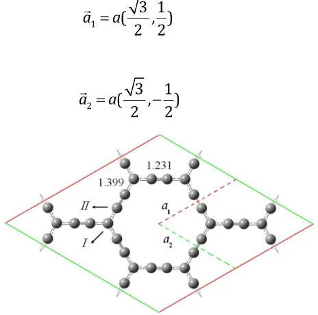
First, the electronic properties of an intrinsic α-graphyne sheet were studied. The 2×2 supercell with 32 carbon atoms was considered to simulate graphyne sheet (Fig. 1). In this figure, the unit cell of α-graphyne which consists of 8 carbon atoms was defined by the primitive lattice vectors:
1
3 1
( , )
2 2
a a (1)
and
2 ( 3, 1)
2 2
a a (2)
Figure 1. Atomic structure of a supercell of α-graphyne.
14
Jo
u
rn
a
l
o
f
M
a
th
e
m
a
ti
c
a
l
N
a
n
o
S
c
ie
n
c
e
Figure 2. Electronic band structure and DOS of monolayer α-graphyne [35].
3.2 Doped monolayer α-graphyne
The α-graphyne doped with impurity was modeled by replacing one of C atoms with one impurity atom (B, N, or O). It means 3.1% impurity was introduced in graphyne. We have considered two different doping sites labeled by I and II in Fig. 1.
One B atom that substitutes one C atom lacks one electron to complete the bonding with its all neighbors. It means B impurity creates additional holes in the valence band. As shown in Fig. 3, linear dispersion near Dirac cone is not destroyed. The Fermi level was shifted significantly due to electron acceptor character of B atom and an energy band gap was introduced around the Dirac point. As a result of B doping, an unoccupied acceptor level is created close to the top edge of the valence band. Hence, B doping changes the behavior of α-graphyne from semimetal to p-type semiconductor [35].
15
Jo
u
rn
a
l o
f
M
a
th
e
m
a
ti
c
a
l N
a
n
o
S
c
ie
n
c
e
The N or O atoms may also enter to the α-graphyne by replacing one C atom. These impurities that enhance the carrier density by contributing additional electrons to the conduction band are called donor. On account of having these extra electrons for the purpose of conduction, the N-doped and O-doped graphyne become n-type semiconductors. In the n-type semiconductor, the donor levels, located closely below the lower edge of the conduction band, are the top occupied levels. In Fig. 4 and Fig. 5, the electronic band structures and DOSs of N-doped and O-doped graphynes with impurity atom in site I are presented,
Figure 4. Electronic band structure and DOS of N-doped α-graphyne [35].
Figure 5. Electronic band structure and DOS of O-doped α-graphyne [35].
3.3 BN doped bilayer α-graphyne
16
Jo
u
rn
a
l
o
f
M
a
th
e
m
a
ti
c
a
l
N
a
n
o
S
c
ie
n
c
e
usual Bernal AB-stacking. This arrangement is commonly found in nature [36], and previous calculations were shown that it is the most energetically favorable configuration [37]. Similarly, a bilayer graphyne with two graphyne layers placed on top of the center of each other were considered (Fig. 6). The BN-doped bilayers were modeled by replacing one of the carbon atoms of the first layer by a B atom and putting a N atom instead one of the carbon atoms of the second layer. It means 3.1% B in the first layer and 3.1% N in the second layer were doped [39].
Figure 6. Atomic structure of bilayer α-graphyne [39].
The electronic band structure and DOS of the bilayer α-graphyne are presented in Fig. 7. As shown, two nearly parallel valence bands (π1and π2levels) are presented
below two nearly parallel conduction bands ( * 1
π and
* 2
π levels). Similar to the monolayer α-graphyne, the lowest conductance band and highest valence band cross each other at the K point and the DOS is zero at the Fermi energy. Interestingly, the bilayer α-graphyne is also a semimetal with no energy gap and zero DOS [38, 39].
17
Jo
u
rn
a
l o
f
M
a
th
e
m
a
ti
c
a
l N
a
n
o
S
c
ie
n
c
e
To clarify the effect of BN doping on the electronic properties of the bilayer graphyne, the electronic band structure and DOS of bilayer graphyne doped with 3.1% B and 3.1% N impurities are presented in Fig. 8. Because of the presence of B and N impurities, one unoccupied level and one occupied level are created close to the Fermi energy, respectively. A small band gap opens in the presence of these impurities and BN-dopedbilayer graphyne is a semiconductor [39].
Figure 8. Electronic band structure and DOS of BN-doped bilayer α-graphyne [39].
3.4 Adsorption of organic molecule
18
Jo
u
rn
a
l
o
f
M
a
th
e
m
a
ti
c
a
l
N
a
n
o
S
c
ie
n
c
e
Figure 9. Atomic structures of α-graphyne in the presence of 1 and 9 TCNE molecules
[40].
Figure 10. Electronic band structures and DOS of α-graphyne in the presence of 1 TCNE molecule [40].
3.5 Functionalization
Atomic structure of α-graphyne with one CCl2 molecule is shown in Fig. 11. The
electronic band structures and DOS of α-graphyne with CCl2 molecule was studied to
clarify the possibility of using functionalization for band gap opening in α-graphyne. As an example, the electronic band structure and DOS of functionalized α-graphyne with a single CCl2 molecule were shown in Fig. 12. Upon CCl2 adsorption, energy band
gap was opened between the valence and conduction band edges. Hence, α-graphyne functionalized with a single CCl2 molecule show semiconducting properties. Here, the
hybridization state of C atoms with CCl2 molecules attached to them was transformed
from sp2 into sp3 and opened the band gap in α-graphyne. It was also found that the
19
Jo
u
rn
a
l o
f
M
a
th
e
m
a
ti
c
a
l N
a
n
o
S
c
ie
n
c
e
Figure 11. Atomic structures of functionalized α-graphyne with four CCl2 molecules [42].
Figure 12. Electronic band structures and DOS of α-graphyne with one CCl2 molecules [42].
4. Conclusions
We have reviewed different possible methods for modifying the electronic properties of α-graphyne. Opening band gap in α-graphyne with doping, adsorption of organic molecule, and chemical functionalization was investigated. The energy band gap and
DOS were calculated by DFT. It was found that monolayer and bilayer α-graphyne
sheets are semimetals. They show semiconducting properties when doped (with B, N, or O), functionalized with CCl2, or TCNE molecule adsorbed on them. The results
20
Jo
u
rn
a
l
o
f
M
a
th
e
m
a
ti
c
a
l
N
a
n
o
S
c
ie
n
c
e
REFERENCES
[1] M.S. Dresselhaus, G.Dresselhaus, and P. Avouris, Carbon Nanotubes: Synthesis, Structure, Properties, and Applications, Springer-Verlag Berlin Heidelberg (2001).
[2] K.S. Novoselov, A.K. Geim, S.V. Morozov, D. Jang, Y. Zhang, S.V. Dubonos, I.V. Grigorieva, and A.A. Firsov, Electric Field Effect in Atomatically Thin Carbon Films, Science 306 (2004) 666.
[3] A.K. Geim, and K.S. Novoselov, The Rise of Grapheen, Nat. Mater. 6 (2007) 183.
[4] A.K. Geim, Graphene Status and Prospects, Science 324 (2009) 1530.
[5] S. Jalili, and R. Majidi, The Effect of Gas Adsorption on Carbon Nanotubes Properties, J. Comput. Theor. Nanosci. 3 (2006) 664.
[6] A.L. Ivanovskii, Graphynes and Graphdyines, Progress in Solid State Chemistry, 41 (2013) 1.
[7] R.H. Baughman, H. Eckhardt, and M. Kertesz, Structure-Property Predictions for New Planar Forms of Carbon: Layered Phases Coating sp2 and sp Atoms, J. Chem. Phys.
87 (1987) 6687.
[8] S.W. Cranford, and M.J. Buehler, Mechanical Properties of Graphyne, Carbon 49 (2011) 4111.
[9] B.G. Kim, and H.J. Choi, Graphyne: Hexagonal Network of Carbon with Versatile Dirac Cones, Phys. Rev. B 86 (2012) 115435.
[10] D. Malko, C. Neiss, F. Viñes, and A. Görling, Completition for Graphene: Graphynes with Direction-Dependent Dirac Cones, Phys. Rev. Lett. 108 (2012) 086804.
[11] D. Haberer, D.V. Vyalikh, S. Taioli, B. Dora, M. Farjam, J. Fink, D. Marchenko, T. Pichler, K. Ziegler, S. Simonucci, M.S. Dresselhaus, M. Knupfer, B. Büchner, and A. Grüneis, Tunable Band Gap in Hydrogenated Quasi-Free-Standing Graphene, Nano Lett. 10 (2010) 3360.
[12] J. Nilsson, and A.C. Neto, Impurities in a Biased Graphene Bilayer,Phys. Rev. Lett. 98 (2007) 126801.
[13] T. Ohta, A. Bostwick, T. Seyller, K. Horn, and E. Rotenberg, Controlling the Electronic Structure of Bilayer Graphene,Science 313 (2006) 951.
21
Jo
u
rn
a
l o
f
M
a
th
e
m
a
ti
c
a
l N
a
n
o
S
c
ie
n
c
e
[15] P. Shemella, and S.K. Nayak, Electronic Structure and Band-Gap Modulation of Graphene via Substrate Surface Chemistry, Appl. Phys. Lett. 94 (2009) 032101.
[16] K. Novoselov, Graphene: Mind the Gap, Nature Matter 6 (2007) 720.
[17] X. Li, X. Wang, L. Zhang, S. Lee, and H. Dai, Chemically Derived, Ultrasmooth Graphene Nanoribbon Semiconductors, Science 319 (2008) 1229.
[18] Y.H. Lu, W. Chen, Y.P. Feng, and P.M. He, Tuning the Electronic Structure of Graphene by an Organic Molecule, J. Phys. Chem. B 113 (2009) 2.
[19] M. Chi, and Y-P, Zhao, First principle study of the interaction and charge transfer between graphene and organic molecules, Comp. Mat. Sci. 56 (2012) 79.
[20] X. Wang, X. Li, L. Zhang, Y. Yoon, P.K. Weber, H. Wang, J. Guo, and H. Dai, N-Doping of Graphene Through Electrothermal Reactions with Ammonia, Science (2009) 768.
[21] T.B. Martins, R.H. Miwa, A.J.R. da Silva, and A. Fazzio, Electronic and Transport Properties of Boron-Doped Graphene Nanoribbons, Phys. Rev. Lett. 98 (2007) 196803(1-4).
[22] D.C. Elias, R.R Nair, T.M.G. Mohiuddin, S.V. Morozov, P. Blake, M.P. Halsall, A.C. Ferrari, D.W. Boukhvalov, M.I. Katsnelson, A.K. Geim, and K.S. Novoselov, Control of Graphene's Properties by Reversible Hydrogenation: Evidence for Graphane, Science 323 (2009) 610.
[23] R.R. Nair, W. Ren, R. Jalil, I. Riaz, V.G. Kravets, L. Britnell, V.G. Kravets, L. Britnell, P. Blake, F. Schedin, A.V. Mayorov, S. Yuan, M.I. Katsnelson, H.M. Cheng, W. Strupinski, L.G. Bulusheva, K.S. Novoselov, and A.K. Geim, Fluorographene: A Two-Dimensional Counterpart of Teflon, Small 6 (2010) 2877.
[24] L. Wang, Y.Y. Sun, K. Lee, D. West, Z.F. Chen, J.J. Zhao, and S.B. Zhang, Stability of Graphene Oxide Phases from First-Principles Calculations, Phys. Rev. B 82 (2010) 161406.
[25] Z. Xu, and K. Xue, Engineering Graphene by Oxidation: A First-Principles Study, Nanotechnol. 21 (2010) 045704.
[26] J-X. Zhao, H-X. Wang, B. Gao, X-G. Wang, Q-H. Cai, and X-Z. Wang, Chemical Functionalization of Graphene via Aryne Cycloaddition: A Theoretical Study, J. Mol. Model, 18 (2012) 2868.
22
Jo
u
rn
a
l
o
f
M
a
th
e
m
a
ti
c
a
l
N
a
n
o
S
c
ie
n
c
e
[28] M. Farjam, and R. Rafii-Tabar, Bandgap Opening of Bilayer Graphene by Dual Doping from Organic Molecule and Substrate, Phys. Rev. B. 80 (2009) 167401 (1-3).
[29] M. Mohr, K. Papageelis, J. Maultzsch, and C. Thomsen, Two-Dimensional Electronic and Vibrational Band Structure of Uniaxially Strained Graphene from ab
initio Calculations, Phys. Rev. B 80 (2009) 205410 (1-4).
[30] S.M. Choi, S.H. Jhi, and Y.W. Son, Effects of Strain on Electronic Properties of Graphene, Phys. Rev. B 81 (2010) 081407 (1-4).
[31] R. Majidi, and K. Ghafoori Tabrizi, Electronic Properties of Defect-Free and Defective Bilayer Graphene in an Electric Field, Fuller. Nanotub. Car. N. 19 (2011) 532.
[32] T. Ozaki, H. Kino, J. Yu, M.J, Han, N. Kobayashi, and M. Ohfuti, et al. (2011) User’s manual of OpenMX version 3.6. http://www.openmx-square.org.
[33] J.P. Perdew, K. Burke, and M. Ernzerhof, Generalized Gradient Approximation Made Simple, Phys. Rev. Lett. 77 (1996) 3865.
[34] S. Grimme, Band Gap Modulation of Graphyne via Chemical Functionalization: A Density Functional Theory Study, J. Comput. Chem. 27 (2006) 1787.
[35] R. Majidi, Effect of Doping on the Electronic Properties of Graphyne, Nano 8 (2013) 1350060.
[36] A.H. Castro Neto, F. Guinea, N.M.R. Peres, K.S. Novoselov, and A.K. Geim, The Electronic Properties of Graphene, Rev. Mod. Phys. 81 (2009) 109.
[37] S.B. Trickey, F. Muller-Plathe, G.H.F. Diercksen, and J.C. Boettger, Interplanar Binding and Lattice Relaxation in a Graphite Dilayer, Phys. Rev. B 45 (1992) 4460.
[38] R. Majidi, and A.R. Karami, Electronic Properties of Bilayer and Trilayer Graphyne in the Presence of Electric Field, Struct. Chem. 25 (2014) 853.
[39] R. Majidi, and A.R. Karami, A Biosensor for Hydrogen Peroxide Detection based on Electronic Properties of Carbon Nanotubes, Mol. Phys. 111 (2013) 3194.
[40] R. Majidi, A.R. Karami, Band Gap Opening in α-Graphyne by Adsorption of Oranic Molecule, Physica E 63 (2014) 264.
[41] R. Majidi, and A.R. Karami, Band Gap Modulation of Graphene and Graphyen via Tetracyanoethylene Adsorption, Studia. UBB. Chemia. 1 (2016) 177.
![Figure 2. Electronic band structure and DOS of monolayer α-graphyne [35].](https://thumb-us.123doks.com/thumbv2/123dok_us/10065520.1992914/4.612.196.415.519.675/figure-electronic-band-structure-dos-monolayer-a-graphyne.webp)
![Figure 4. Electronic band structure and DOS of N-doped α-graphyne [35].](https://thumb-us.123doks.com/thumbv2/123dok_us/10065520.1992914/5.612.206.405.445.609/figure-electronic-band-structure-dos-n-doped-graphyne.webp)
![Figure 7. Electronic band structure and DOS of bilayer α-graphene [38, 39].](https://thumb-us.123doks.com/thumbv2/123dok_us/10065520.1992914/6.612.199.408.477.651/figure-electronic-band-structure-dos-bilayer-a-graphene.webp)
![Figure 8. Electronic band structure and DOS of BN-doped bilayer α-graphyne [39].](https://thumb-us.123doks.com/thumbv2/123dok_us/10065520.1992914/7.612.195.411.217.384/figure-electronic-band-structure-dos-doped-bilayer-graphyne.webp)
![Figure 9. Atomic structures of α-graphyne in the presence of 1 and 9 TCNE molecules [40]](https://thumb-us.123doks.com/thumbv2/123dok_us/10065520.1992914/8.612.182.430.268.438/figure-atomic-structures-a-graphyne-presence-tcne-molecules.webp)
![Figure 11. Atomic structures of functionalized α-graphyne with four CCl2 molecules [42]](https://thumb-us.123doks.com/thumbv2/123dok_us/10065520.1992914/9.612.175.436.263.471/figure-atomic-structures-functionalized-a-graphyne-ccl-molecules.webp)
