DESIGN AND STABILITY ANALYSIS TECHNIQUES
FOR SWITCHING-MODE NONLINEAR CIRCUITS:
POWER AMPLIFIERS AND OSCILLATORS
Thesis by
Sanggeun Jeon
In Partial Fulfillment of the Requirements
for the Degree of
Doctor of Philosophy
CALIFORNIA INSTITUTE OF TECHNOLOGY
Pasadena, California
2006
ii
© 2006
Sanggeun Jeon
iii
Acknowledgements
First, I would like to thank my advisor, Prof. David Rutledge, for giving me this
opportunity to pursue the Ph.D. at Caltech as a member of his research group. In addition to
his keen advice and guidance, the kind support and encouragement that he showed me make
this thesis possible.
I am equally grateful to Prof. Almudena Suárez who guided and taught me with her
endless passion and expertise. Without her technical guidance, any part of this thesis would
not be possible. It was such a pleasant and enlightening experience to work under her tutelage
and encouragement.
I also want to thank Dr. Sander Weinreb for his valuable advice and suggestions given
during the weekly group meeting and Prof. Ali Hajimiri, Prof. Daniel Stancil, and Prof. John
Doyle for serving on my defense committee.
I was glad to have the opportunity to work with many talented people on 4th floor,
Moore laboratory. Special thanks should be given to Kent Potter for his unfailing advice on
building practical circuits in the laboratory. Dr. Feiyu Wang deserves much credit for
valuable discussions on switching-mode amplifiers from which I got many ideas. My
research and life at Caltech were also enriched by many conversations and discussions with
my friends in the RF/Microwave group, including Dr. Lawrence Cheung, Dr. Matthew
Morgan, Dr. Dai Lu, Dr. Seonghan Ryu, Dr. Younkyu Chung, Min Park, Niklas Wadefalk,
Ann Shen, Patrick Cesarano, Yulung Tang, Guangxi Wang, Edwin Seodarmadji, Motofumi
Arii, Rohit Gawandi, Paul Laufer, Glenn Jones, and Hamdi Mani. I’d like to wish all the best
to the new group members, Sebastien Lasfargues and Joe Bardin. I was also pleased to have
many chances to talk with visitors to this group: Prof. Yoshizumi Yasuoka and Prof. Yoshio
iv
Patama Taweesup for their continuous support and help. Dale told me many interesting
stories and gave me advice useful in life at Caltech.
I would like to express many thanks to George Sopp, Jennifer Arroyo, Rick Nicklaus,
and Dr. Cynthia Hang at Raytheon, as they gave me the opportunity to work with them and to
successfully apply the techniques developed in this thesis to industrial sections.
I also want to thank Dr. Franco Ramirez, Dr. Sergio Sancho, Ana Collado, Dr. Apostolos
Georgiadis, and Prof. Juan-Mari Collantes for their kind hospitality and technical discussions
during my stay in Santander. Especially, Prof. Juan-Mari Collantes deserves special credit for
the development of stability analysis tools, without which my stability work would not be
possible.
I am deeply grateful to my parents, Young-Tae Jeon and Pil-Rye Kim, and my departed
grandmother, Im Kang. Without their endless inspiration and dedicated support, I would not
have achieved this goal in my life. To my sisters, Seo-Young and Hye-Sook, and my brother,
Hyung-Geun, I give thanks for their love and encouragement. Finally, I would like to thank
my wife, Hyekyung, for her unlimited patience and encouragement, which has been the
greatest source of energy for me to keep going forward during the entire of this work. She has
gone through many challenges along with me including giving birth to our son, Heesoo
v
Abstract
A design technique for kW-level switching-mode power amplifiers is presented. Several
push-pull pairs, independently tuned to Class-E/Fodd, are combined by a distributed active
transformer. The zero voltage switching (ZVS) condition is investigated and modified for the
Class-E/Fodd amplifier with a non-ideal output transformer. All lumped elements including
the DAT, the transistor package, and the input-power distribution network are modeled and
optimized to achieve the ZVS condition and the high drain efficiency. Two power amplifiers
are implemented at 29 MHz, following the technique. The amplifier with two push-pull pairs
combined exhibits 1.5 kW output power with 85 % drain efficiency and 18 dB gain. When
four push-pull pairs are combined, an output power of 2.7 kW is achieved with 79 % drain
efficiency and 18 dB gain.
Nonlinear stability analysis techniques, based on an auxiliary generator and pole-zero
identification, are introduced to predict and eliminate the instabilities of power amplifiers.
The techniques are applied to two switching-mode power amplifiers that exhibited different
instabilities during the measurements. Self-oscillation, chaos, and hysteresis of a Class-E/Fodd
amplifier with a distributed active transformer are investigated by the stability and bifurcation
analysis tools. An in-depth analysis of the oscillation mechanism is also carried out, which
enables an efficient determination of the topology and location of the required global
stabilization network. As the other application, the anomalous behavior observed in a Class-E
power amplifier is analyzed in detail. It involves hysteresis in the power-transfer curve,
self-oscillation, harmonic synchronization, and noisy precursors. To correct the amplifier
performance, a new technique for elimination of the hysteresis is proposed, based on
bifurcation detection through a single simulation on harmonic-balance software. Also
vi
practical circuits and a technique is derived for their elimination from the amplifier output
spectrum. All of the stabilization and correction of the amplifiers are experimentally validated.
A simple nonlinear technique for the design of high-efficiency and high-power
switching-mode oscillators is presented. It combines existing quasi-nonlinear methods and
the use of an auxiliary generator in harmonic balance. The auxiliary generator enables the
oscillator optimization to achieve high output power and DC-to-rf conversion efficiency
without affecting the oscillation frequency. It also imposes a sufficient drive on the transistor
to enable the switching-mode operation with high efficiency. The oscillation start-up
condition and the steady-state stability are analyzed with the pole-zero identification
technique. The influence of the gate bias on the output power, efficiency, and stability is also
investigated. A Class-E oscillator is demonstrated using the proposed technique. The
vii
Table of Contents
Chapter 1 Introduction ... 1Chapter 2 Design Considerations of Switching-Mode Power Amplifiers... 5
2.1 Performance Criteria of Switching-Mode Power Amplifiers ...7
2.1.1 Efficiency...7
2.1.1.1 Definitions...7
2.1.1.2 Why High Efficiency? ...10
2.1.2 Linearity...11
2.1.3 Output Power ...15
2.1.4 Operating Frequency...16
2.1.5 Gain and Bandwidth ...17
2.2 Operating Classes of Power Amplifiers...18
2.2.1 Transconductance Amplifiers ...19
2.2.1.1 Class-A...19
2.2.1.2 Class-B, AB ...21
2.2.1.3 Class-C...22
2.2.2 Switching-Mode Amplifiers ...22
2.2.2.1 Class-D...23
2.2.2.2 Class-E ...24
2.2.2.3 Class-F ...27
2.2.2.4 Class-E/F...28
2.3 Stability...30
2.3.1 Types of Instabilities...31
2.3.2 Stability Analysis Techniques...34
Chapter 3 Switching-Mode Power Amplifiers for ISM Applications ... 35
viii
3.2 Discrete Implementation of DAT ...38
3.3 1.5-kW, 29-MHz Class-E/Fodd Amplifier with a DAT ...40
3.3.1 Active Device...42
3.3.2 Input-power Distribution Network ...44
3.3.3 Performance Simulation...46
3.3.4 Implementation of the Amplifier ...48
3.3.5 Experimental Results ...49
3.4 2.7-kW, 29-MHz Class-E/Fodd Amplifier with a DAT ...54
3.4.1 Performance Simulation and Implementation ...55
3.4.2 Experimental Results ...56
Chapter 4 Nonlinear Stability Analysis Techniques... 59
4.1 Linear Stability Analysis Techniques ...59
4.2 Nonlinear Stability Analysis Techniques...61
4.2.1 Pole-Zero Identification ...62
4.2.2 Auxiliary Generator ...64
Chapter 5 Global Stability Analysis and Stabilization of a Class-E/F Amplifier with a DAT ... 69
5.1 Instabilities of a Class-E/Fodd Power Amplifier ...70
5.2 Transistor Modeling...73
5.3 Stability Analysis ...74
5.3.1 Local Stability Analysis...74
5.3.2 Instability Contour ...77
5.3.3 Analysis of the Self-Oscillating Mixer Regime...79
5.3.4 Hysteresis Prediction ...83
5.3.5 Envelope-Transient Analysis of the Oscillating Solution...84
5.4 Stabilization Technique ...88
5.5 Measurements of the Stabilized Amplifier ...94
ix
6.1 Experimental Measurements on the Class-E Power Amplifier ...97
6.2 Nonlinear Analysis of the Class-E Power Amplifier...101
6.2.1 Analysis of the Power-Transfer Curve ...101
6.2.2 Stability Analysis ...103
6.2.3 Analysis of the Oscillatory Solution ...107
6.3 Analysis of Noisy Precursors...110
6.3.1 Precursor Model and Analysis Techniques...110
6.3.2 Application to the Class-E Amplifier ...112
6.4 Elimination of the Hysteresis in the Pin-Pout Curve...115
6.5 Elimination of Noisy Precursors...122
Chapter 7 Nonlinear Design Technique for High-Power Switching-Mode Oscillators... 127
7.1 Optimization of Class-E Amplifier and Synthesis of Embedding Network ...129
7.1.1 Optimization of Class-E Amplifier...130
7.1.2 Synthesis of Embedding Network ...133
7.2 Nonlinear Optimization of the Oscillator Performance ...136
7.2.1 Nonlinear Optimization through the AG Technique ...137
7.2.2 Stability Analysis ...140
7.3 Analysis of the Oscillating Solution versus the Gate Bias ...142
7.4 Experimental Results ...149
x
List of Tables
Table 3.1: Extracted result of slab transformer parameters ...40 Table 3.2: Component values of the power amplifier...54 Table 5.1: Phase of signals with different frequencies at each drain terminal of the four
transistors (Vd1 ~ Vd4 are defined in Figure 3.5)...81
Table 7.1: Optimized terminal voltages and currents at fundamental frequency...135 Table 7.2: Evaluated element values of embedding network and corresponding circuit
elements...135
xi
List of Figures
Figure 2.1: Typical power flow in a generalized amplifier. ...8Figure 2.2: Comparison of qualitative power-transfer curves between an ideally linear amplifier (a) and a typical switching-mode amplifier (b)...12
Figure 2.3: Simplified envelope elimination and restoration (EER) system...14
Figure 2.4: Simplified linear amplification using nonlinear components (LINC) system. . ...14
Figure 2.5: Definition of bandwidth in terms of output power. ...18
Figure 2.6: Bias points and load lines of transconductance amplifiers. ...20
Figure 2.7: Drain voltage and current waveforms of ideal Class-A amplifiers...20
Figure 2.8: Drain voltage and current waveforms of ideal Class-B amplifiers...21
Figure 2.9: Drain voltage and current waveforms of ideal Class-C amplifiers...22
Figure 2.10: Drain voltage and current waveforms of ideal Class-D amplifiers...24
Figure 2.11: Basic schematic of a Class-E amplifier. ...26
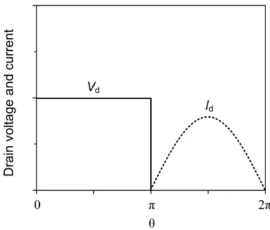
Figure 2.12: Drain voltage and current waveforms of ideal Class-E amplifiers. ...26
Figure 2.13: Drain voltage and current waveforms of ideal Class-F amplifiers. ...27
Figure 2.14: Conceptual schematic of a Class-F amplifier. ...28
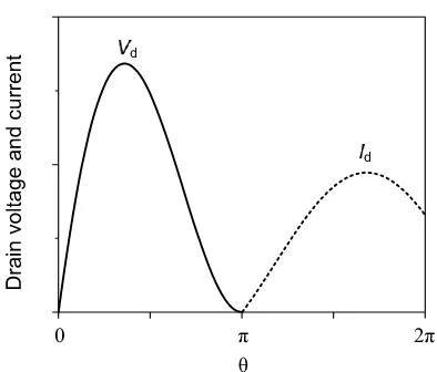
Figure 2.15: Basic schematic of a Class-E/Fodd amplifier. ...29
Figure 2.16: Drain voltage and current waveforms of ideal Class-E/Fodd amplifiers...30
Figure 2.17: Types of instability commonly observed in power amplifiers. (a) Sub-harmonic oscillation. (b) Spurious oscillation at frequency unrelated with the input drive. (c) Chaos. (d) Noisy precursors. (e) Hysteresis and jump of solutions. ...33
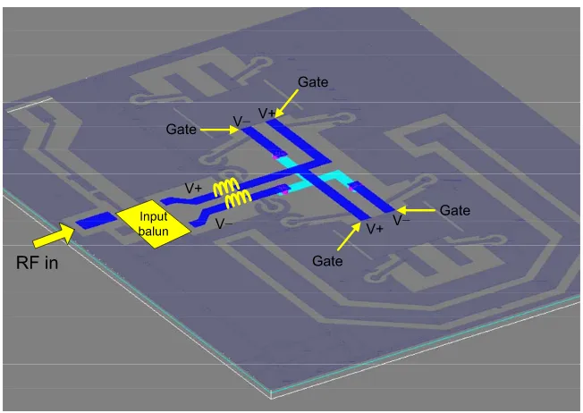
Figure 3.1: A Class-E/Fodd push-pull amplifier with a non-ideal output transformer. ....38
Figure 3.2: Structure of the slab transformer: a section of the DAT...39
xii
Figure 3.4: Measured (symbol) and simulated (line) S-parameters of the slab transformer: slab length of 7.5 cm, 50−200 MHz...40
Figure 3.5: Complete schematic of a 1.5-kW, 29-MHz power amplifier. Desired voltage waveforms at gates and drains are represented...41
Figure 3.6: Simple switch model of the transistor used for amplifier simulation. ...43
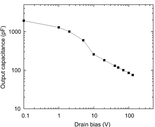
Figure 3.7: Extracted output capacitance of ARF 473 VDMOS...43
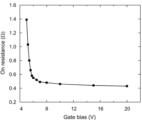
Figure 3.8: Extracted on-resistance of ARF 473 VDMOS...44
Figure 3.9: Input-power distribution network in a multi-layered board. Blue and cyan traces are on the top and middle layers, respectively...45
Figure 3.10: Simulated voltage waveforms at each of four gate terminals fed by input-power distribution network. ...46
Figure 3.11: Simulated output power and drain efficiency versus slab length of the DAT. . ...47
Figure 3.12: Simulated switch voltage and current waveforms for 1.6 kW output power.... ...47
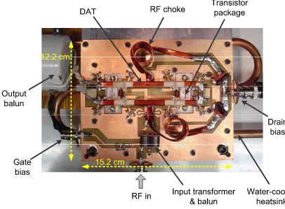
Figure 3.13: Photo of the 1.5-kW, 29-MHz power amplifier...48
Figure 3.14: Block diagram of measurement setup for high-power amplifiers. ...50
Figure 3.15: Photo of the measurement setup. ...50
Figure 3.16: Measured gain and drain efficiency versus output power at 29 MHz. ...52
Figure 3.17: Output power spectrum for 1.5 kW. (a) Measured, (b) Simulated. ...52
Figure 3.18: Measured drain voltage waveforms for 1.5 kW. Two drain terminals in the same push-pull pair are taken. ...53
Figure 3.19: Thermal image of the amplifier driven at 1.5 kW for 30 seconds. ...53
Figure 3.20: Complete schematic of a 2.7-kW, 29-MHz power amplifier...54
Figure 3.21: Photo of the 2.7-kW, 29-MHz power amplifier...55
Figure 3.22: Measured (solid lines) drain voltage waveforms of eight transistors for 2.7 kW output power. Simulated (dotted lines) waveforms of two transistors are superimposed. ...57
xiii
Figure 3.24: Measured output power and input VSWR vs. input frequency for a drain voltage of 72 V...58 Figure 3.25: Measured output power spectrum for 2.7 kW. The harmonics power level is
normalized by the fundamental...58 Figure 4.1: Three common types of bifurcation. (a) Hopf bifurcation. (b) Flip bifurcation. (c) D-type bifurcation. ...62 Figure 4.2: Example of pole-zero identification result...64
Figure 4.3: Schematic for obtaining the impedance function calculated from a
large-signal harmonic balance solution. ...64
Figure 4.4: Implementation of an auxiliary generator in harmonic balance simulation. A
nonlinear circuit is driven by a large input signal of Vin and fin...65
Figure 4.5: Illustrative bifurcation locus traced by the auxiliary generator technique....68
Figure 4.6: Illustrative oscillating solution curve traced by the auxiliary generator
technique. ...68
Figure 5.1: Variation of the output power spectrum when increasing the input power. (a)
Pin= 4 W, showing leakage power at the input-drive frequency. (b)
Pin = 10W, showing a chaotic spectrum. (c) Pin= 16.5 W, showing the
proper spectrum in switching-mode operation. ...72
Figure 5.2: Quasi-periodic output power spectrum observed near the bifurcation
boundary when the input power is decreased. The circuit behaves in a
self-oscillating mixer regime, at the input-drive frequency fin = 29 MHz and the
oscillation frequency fa≈ 4 MHz. ...73
Figure 5.3: Evolution of the critical poles with increasing input power for VDD = 72V.
For simplicity, only poles in the upper half of the complex plane have been represented. The input power has been increased from 5 W to 15 W by 1-W steps...76
Figure 5.4: Instability contour (solid line). The Hopf-bifurcation locus delimits the VDD
and Pin values for which the amplifier periodic solution is unstable.
xiv
border. In the lower border, triangles indicate the onset of instability for increasing input power, whereas stars indicate recovering of stable behavior for decreasing power. The dashed line shows the input power variation in the pole-zero identification of Figure 5.3. Note that both analyses show good consistency in bifurcation points. ...79
Figure 5.5: Comparison of two simulated drain voltage waveforms Vd1 and Vd2 in the
same push-pull pair. ...82
Figure 5.6: Schematic of the push-pull amplifier, showing the virtual-ground and the
virtual-open planes at the oscillation frequency. ...82
Figure 5.7: Simulation of the undesired self-oscillating mixer regime of the PA.
Variation of the oscillation amplitude at the drain terminal is represented with the input-drive power. The points at which the different bifurcations
occur are indicated. H stands for a Hopf bifurcation and T stands for a
turning point. Hl1and Hu1 are Hopf bifurcations from amplifier periodic
regime. Hl2 is a Hopf bifurcation from self-oscillating mixer regime. J1 and
J2 indicate jumps of the solution. Chaotic solutions are observed from Hl2,
which is analyzed in Section 5.3.5...84
Figure 5.8: Envelope-transient simulation of the amplifier. (a) Time-domain evolution
of the magnitude of the fin harmonic component of the drain voltage when a
two-fundamental basis at fin and fa is considered. (b) Spectrum of the
harmonic component, showing the presence of two oscillation frequencies. ...86
Figure 5.9: Expanded view of the experimental output power spectrum about the
input-drive frequency. VDD = 72 V and Pin = 5.15 W. ...87
Figure 5.10: Simplified equivalent circuit of the PA at the oscillation frequency after considering the virtual-open and virtual-ground planes. ...91 Figure 5.11: Amplifier schematic with stabilization network. The stabilization network
consists of a stabilization resistor Rstab, a second harmonic trap, and a
xv
Figure 5.12: Stabilization action of the parallel resistance, analyzed by means of admittance plots. Three resistance values have been considered. (a) No stabilization resistor. (b) Rstab = 100 Ω. (c) Rstab = 50 Ω. (d) Rstab = 15 Ω. In
(a), (b), and (c), the oscillation condition is satisfied for a certain parameter range, and thus the global stability is not achieved. ...92
Figure 5.13: Variation of the maximum value of stabilization resistance R0stab versus the
input-drive power Pin, obtained through bifurcation analysis. Three different
drain bias voltages have been considered. ...93 Figure 5.14: Variation of the amplifier drain efficiency and output power versus the value
of the stabilization resistance. The drain bias voltage is assumed as
VDD = 72 V. ...93
Figure 5.15: Measured drain efficiency versus the output power. Solid line: the stabilized PA, dashed line: the original PA...94
Figure 6.1: Schematic of the Class-E power amplifier at 7.4 MHz [35]...99
Figure 6.2: Measured output power spectrum of the Class-E power amplifier, for
different input power values. Resolution bandwidth = 3 kHz. (a) Pin = 0.5 W.
Pronounced noise bumps are observed about the frequencies fc = 560 kHz
and fin±fc. (b) Pin = 0.8 W. The bump frequency fc is lower and its power is
higher. (c) Pin = 0.83 W. An oscillation suddenly arises at the frequency
fa = 1 MHz. (d) Pin = 0.89 W. Frequency division by 7. The seventh
harmonic of the oscillation is synchronized to the input frequency. (e) Pin =
4.0 W. Proper operation of the amplifier. ...100
Figure 6.3: Multi-valued Pin-Pout curve of the Class-E power amplifier, obtained with
the AG-based switching-parameter technique. The section in which the amplifier behaves in self-oscillating mixer regime is indicated by stars. ...103
Figure 6.4: Pole evolution along the Pin-Pout curve of Figure 6.3. (a) Section ζ1-ζ2-ζ4 of
Figure 6.3. The two pairs of poles σ1 ± j2πf1 andσ2 ± j2πf2 closest to the
imaginary axis are represented. (b) Section ζ2-T1-ζ3. The complex-conjugate
xvi
two different real poles, γ1, γ2 and, from that point, follow opposite
directions. One of the real poles crosses the imaginary axis at Pin = 0.790 W,
corresponding to the turning point T1, and the solution becomes unstable.
(c) Section ζ3-T2-H1-ζ4-ζ5. The real poleγ1 crosses the imaginary axis back
to the left-hand side at Pin = 0.777 W, corresponding to the turning point T2.
The pair of complex-conjugate poles σ2 ± j2πf2 crosses the imaginary axis to
the right-hand side at the Hopf bifurcation H1, obtained for Pin = 0.781 W.
...105
Figure 6.5: Bifurcation diagram of the Class-E power amplifier versus the input power
Pin. The dashed curve represents the output power of the unstable periodic
solution. For the self-oscillating mixer regime, the power variations at both the oscillation frequency and input-drive frequency are represented. The turning points and Hopf bifurcations are also indicated. ...109
Figure 6.6: Synchronization diagram versus Pin for frequency division by 7. The closed
curve with butterfly shape represents the synchronized solution. This solution is unstable in the dashed-line sections. The power at the oscillation frequency, outside the synchronization region, is also traced. ...109
Figure 6.7: Validation of sideband amplification. Frequency variation of the current gain
from the channel-noise current source to the amplifier output, calculated
with the conversion matrix. Three different Pin values have been considered.
...114
Figure 6.8: Analysis of noisy precursors. Comparison of the simulated output spectrum
using the conversion-matrix and the envelope-transient methods. Higher power is obtained at the upper sideband, in agreement with the higher gain value obtained in Figure 6.7...115
Figure 6.9: Locus of turning points in the plane defined by the stabilization parameter
Clpf and the input power Pin. The two power values obtained for each Llpf and
Clpf correspond to the two turning points of Pin-Pout curves, like the ones in
xvii
no turning points are obtained and no hysteresis phenomenon is observed. ...120
Figure 6.10: Elimination of the hysteresis phenomenon, with Llpf = 257 nH. The
hysteresis interval becomes narrower as the capacitance Clpf is reduced, in
agreement with the loci in Figure 6.9. For capacitor values smaller than
Clpf = 85 pF, corresponding to the cusp point of this locus, no hysteresis is
observed. ...121
Figure 6.11: Variation of the real pole γ1 versus the input-drive power for different values
of the capacitance Clpf. At the cusp point, the curve is tangent to the
horizontal axis...121
Figure 6.12: Measured Pin-Pout transfer characteristics before and after the elimination of
the hysteresis. For the stabilized PA, only the curves without oscillation are presented. ...122 Figure 6.13: Corrected amplifier. Frequency variation of the current gain from the
channel-noise current source to the circuit output, calculated with conversion matrix. ...124 Figure 6.14: Simulated output power spectrum of the corrected amplifier, in which no
noise bumps are observed. ...125
Figure 6.15: Measured output power spectrum of the corrected amplifier at Pin = 0.95 W.
The noise from the input-drive source is still present about fin. However, the
noise bumps have disappeared, which validates the proposed correction technique. ...125 Figure 6.16: Comparison of the measured gain and drain efficiency versus the output
power between the original and corrected amplifiers. The input power is 9 W for saturated switching operation in the entire measurements. ...126
Figure 7.1: Schematic of the Class-E amplifier. The input-drive frequency is set to the
oscillation frequency. TLin is a transmission line added at the gate to
xviii
Section 7.1.2. Dashed lines represent the reference planes for the synthesis. ...131
Figure 7.2: Simulated output power (a) and drain efficiency (b) of the Class-E amplifier
as functions of detuning inductance and load resistance. The drain and gate bias voltages are 25 V and 4 V, respectively. ...132
Figure 7.3: Simulated output power and drain efficiency as a function of the input-drive
level Vin. Ldetune and RL are tuned to the maximum drain efficiency point. The
dotted line at 40 V represents the determined input-drive level for the
saturated operation. ...132
Figure 7.4: Basic structure of the Class-E oscillator, consisting of a transistor, a series
LC tank, and an embedding network. The embedding network substitutes for the input-drive source and output load circuitry of the Class-E amplifier in Figure 7.1, keeping the same set of terminal voltages and currents. ...134
Figure 7.5: Complete schematic of the Class-E oscillator. The embedding network is
implemented by capacitors (C2, C3, Co), transmission lines (TLind, TLo), and
a 50 Ω load (RL). The AG, consisting of a voltage source and an ideal
bandpass filter inside the dashed box, is not a part of the oscillator, but will be used for the nonlinear simulation of oscillatory solutions in Section 7.2. ...136
Figure 7.6: Contour plots of the simulated DC-to-rf conversion efficiency (a) and output
power (b) in the plane of (C2, C3). For the entire solutions, the oscillation
frequency is fixed to 410 MHz. The points of a star and a square represent,
respectively, the original values of (C2, C3) obtained in Section 7.1 and the
new values nonlinearly optimized in the output power and efficiency. ...139
Figure 7.7: Simulated voltage and current waveforms at the extrinsic drain terminal,
xix
Figure 7.8: Evolution of the critical pole pair with the values of C2 and C3 varied along
the dashed line in Figure 7.6. C2 is varied from 1 pF to 9 pF in steps of 1 pF
along the dashed line and the corresponding value of C3 is calculated from
the dashed-line equation. At each point of (C2, C3), pole-zero identification
is carried out on the input impedance function, which is obtained from the linearized DC solution. ...142
Figure 7.9: Simulated output power and DC-to-rf conversion efficiency in the
oscillatory regime as a function of the gate bias voltage. Four drain bias
voltages (Vdd) are considered. The solid-line and dashed-line sections
represent the stable and unstable oscillating solutions, respectively, in each solution curve...144 Figure 7.10: Evolution of the critical pole pair for the steady-state oscillating solution as
the gate bias varies from the stable section to the unstable one near the turning point in Figure 7.9. The solid squares close to the imaginary axis represent another pair of complex-conjugate poles at each bias point, exhibited due to the singularity of the HB system for oscillating solutions. ...145 Figure 7.11: Gate voltage waveforms at different gate bias voltages. The threshold
voltage is represented by a thin solid line. The considered drain bias is 25 V. ...146 Figure 7.12: Simulated evolution of the oscillating solution as the gate bias changes from
4 V to different values. The fundamental component of the voltage at the
AG connection node is represented. The AG is disconnected at 0.1 μs. The
considered drain bias is 25 V. ...148 Figure 7.13: Photo of the Class-E oscillator built on FR-4 board. The transistor is
mounted directly on a heatsink through a slot in the board. The circuit size is 49 mm x 35 mm. ...150 Figure 7.14: Measured output power and DC-to-rf conversion efficiency versus the drain
xx
Figure 7.15: Measured output power and DC-to-rf conversion efficiency versus the gate bias voltage. The applied drain bias voltage is 23 V. ...152 Figure 7.16: Measured and simulated output power spectrum. The largest harmonic is the
second, at 46 dB below the fundamental. ...152
Figure 8.1: Comparison of simulated output power (a) and efficiency (b) between a
1
Chapter 1
Introduction
The tremendous expansion of wireless communications in the 21st century pushes the
performance of each component of communication systems to more and more stringent
specifications. In power amplifiers, the performance issues include efficiency, linearity,
output power, and spectral purity. In particular, the efficiency has been of great significance
to power amplifier designers because it affects the lifetime, reliability, and cost of the entire
system. This is also the situation for power amplifiers in industrial, scientific, and
medical (ISM) applications such as induction heating, plasma generation, RF-driven lighting,
or RF imaging.
Switching-mode amplifiers such as Class-D, E, F, and E/F have been proposed in the
context of the demand for high-efficiency power amplifiers. They achieve the high efficiency
at the expense of linearity, through the switching operation of the transistor and the
appropriate harmonic tuning of output impedance. Recent advances in transistor technology
enable the switching-mode concepts to be extended to the applications of higher output
power as well as higher frequency. However, it is still challenging to build solid-state power
amplifiers with several kW output power for ISM applications, although in comparison with
vacuum-tube power amplifiers, they would have light weight, compact size, and high
reliability. Judicious selection of the solid-state device and the operating mode of
amplification should be made in order to generate and handle enormous voltage and current
at the output. Also, a very efficient technique for power combining is required to achieve
several kW from solid-state devices, since it is difficult to obtain such a high power level
2
Stability is an important design issue in all types of RF and microwave circuits.
Instabilities, such as spurious oscillations, noisy precursors, chaos, hysteresis, solution jumps,
etc., degrade or disrupt the original performance of each circuit. They also may destroy the
active device itself due to the excessive terminal voltage or current induced from its abnormal
operation. The stability analysis of switching-mode power amplifiers is especially essential
because of their strongly nonlinear operating behavior, which gives many more possibilities
for instability. Unfortunately, most of these instabilities come from parametric oscillations
and are difficult to predict by conventional linear stability analysis techniques. Instead,
nonlinear techniques, taking into account the steady-state solution driven by large input
signal, are required in order to detect and remedy such parametric instabilities. To be
practical, the techniques should be general enough to be applied to any kind of amplifiers and
should be implemented on commercial harmonic balance simulators.
This dissertation presents design and implementation techniques for solid-state power
amplifiers that generate the output power up to 2.7 kW. Several vertically double-diffused
MOS (VDMOS) are tuned to Class-E/Fodd mode [1] to achieve high efficiency. The output
power from each VDMOS is then combined using a distributed active transformer (DAT) [2].
The amplifier with four VDMOS combined exhibits 1.5 kW output power with 85 % drain
efficiency and 18 dB gain at 29 MHz. The output power of 2.7 kW is achieved with 79 %
drain efficiency and 18 dB gain, when eight VDMOS are combined by the DAT.
Motivated by common observation of various instabilities during the measurements of
switching-mode amplifiers, this dissertation presents nonlinear approaches for stability
analysis of power amplifiers. Based on bifurcation detection tools including pole-zero
identification and an auxiliary generator, the region for stable operation is delimited with
respect to circuit parameters of interest. These tools are implemented in a commercial
harmonic balance simulator with an optimization engine. Different instabilities are also
analyzed in a large-signal operating regime by combining the bifurcation detection tools with
3
simulation. All of these stability analysis techniques are applied to stabilize two
switching-mode amplifiers that have shown various instabilities: spurious oscillation,
hysteresis of the oscillating solution, and chaotic spectrum in a Class-E/Fodd amplifier, and
noisy precursors and hysteresis of the power-transfer curve in a Class-E amplifier. These
instabilities are predicted, analyzed, and finally eliminated in a global manner of operation,
using the stability analysis techniques.
Interestingly, the nonlinear stability analysis is beneficial not only to suppressing critical
instabilities in power amplifiers, but also to promoting desirable oscillations in other
nonlinear circuits such as oscillators or synchronized circuits. This dissertation also presents a
nonlinear design technique for high-power switching-mode oscillators, based on the stability
analysis tools. By combining existing quasi-nonlinear design techniques with an auxiliary
generator, a switching-mode oscillator can be designed, such that the output power and
efficiency are optimized at a fixed oscillation frequency. Intensive stability analyses are
carried out for oscillation start-up and steady-state solutions using pole-zero identification.
The technique is experimentally verified by the design of a Class-E oscillator at 410 MHz.
This dissertation is based on the following published work:
S. Jeon, A. Suárez, and D. B. Rutledge, “Nonlinear design technique for high-power
switching-mode oscillators,” IEEE Trans. Microwave Theory & Tech., accepted for
publication.
S. Jeon, A. Suárez, and D. B. Rutledge, “Analysis and elimination of hysteresis and noisy
precursors in power amplifiers,” IEEE Trans. Microwave Theory & Tech., vol. 54, no. 3, pp.
1096−1106, Mar. 2006.
S. Jeon, A. Suárez, and D. B. Rutledge, “Global stability analysis and stabilization of a
Class-E/F amplifier with a distributed active transformer,” IEEE Trans. Microwave Theory &
4
S. Jeon and D. B. Rutledge, “A 2.7-kW, 29-MHz class-E/Fodd amplifier with a distributed
active transformer,” 2005 IEEE MTT-S Int. Microwave Symp. Dig., Long Beach, CA, Jun.
5
Chapter 2
Design Considerations of
Switching-Mode Power Amplifiers
Power amplifiers are widely used in the applications of wireless communication, radar,
and industrial, scientific, and medical (ISM) fields. In wireless communication and active
radar applications, power amplifiers amplify different RF input signals, depending on the
modulation scheme, to feed sufficient transmitting power to antennas. ISM applications such
as induction heating, plasma generation, RF-driven lighting, or imaging require RF power
sources that generate a significant amount of RF power.
Since each application has a different operating condition and requirement of the power
amplifier, no single or unified technique exists for the optimum design that is suitable for all
applications. Designers have to consider the important performance issues of the power
amplifier for a particular application. Then, they select or invent appropriate components and
techniques at every design step, from the choice of transistors to the entire architecture. This
custom-fit property makes a power amplifier one of the most expensive blocks in a whole
system of applications.
Switching-mode power amplifiers have been proposed and developed for the
applications that require high efficiency. By operating the transistor as a switch rather than a
current source and employing appropriate output harmonic terminations, the amplifiers can
achieve 100 % efficiency in principle. The linearity of switching-mode amplifiers, however,
6
applications of switching-mode amplifiers are RF power generation systems in ISM fields
and communication systems modulated with a constant-envelope signal.
There are many design considerations to be addressed for the switching-mode power
amplifiers. Proper choice of operating class, transistors, power-combining technique, and
thermal management must be done, based on the performance criteria required for each
particular application. The criteria include operating frequency, output power level,
bandwidth, gain, and stability as well as efficiency and linearity.
A difficult situation frequently encountered in the switching-mode power amplifier
design is that the strongly nonlinear operating nature of the amplifiers usually puts more
challenges to meeting all of the required specifications. For instance, the nonlinear behavior
of the transistor not only degrades the linearity demanded for communication systems with
non-constant envelope modulation scheme [3], but also gives much possibility to induce
instabilities [4] that are detrimental to both the amplifier and the whole system. These
instabilities are generated in the large-signal operating regime of the amplifiers, so that they
are extremely difficult to predict and (or) eliminate by using conventional small-signal
stability analysis such as k-factor or stability circles.
Moreover, there exist some inherent trade-offs between performance criteria of power
amplifiers: efficiency and linearity, operating frequency and gain, operating frequency and
output power, bandwidth and gain, etc. These trade-offs are also applied to switching-mode
power amplifiers in the same way. Designers usually optimize one criterion of performance
while sacrificing the other but keeping it within an acceptable level, depending on the
applications. Thus, the design of power amplifiers demands a wide view of all criteria
involved in the requirements as well as a careful application of detailed design techniques.
This chapter discusses the main design issues and considerations for switching-mode
7
be dealt with first, and then followed by the technologies and considerations involved with
the switching-mode amplifier design.
2.1
Performance Criteria of Switching-Mode
Power Amplifiers
There are numerous criteria to evaluate the performance of switching-mode power
amplifiers. The most significant criterion is obviously the efficiency, which is why the
switching-mode techniques have been proposed. At the expense of linearity, the amplifiers
can achieve high efficiency, ideally up to 100 % from their deeply saturated operation.
Operating frequency, output power, gain, and bandwidth should also be considered at the
design stage in order to choose proper active devices or design technologies. In this section,
major performance criteria in switching-mode power amplifiers are reviewed.
2.1.1
Efficiency
2.1.1.1 Definitions
An amplifier is not a magical circuit that amplifies an RF input signal to a larger level
without any additional power input. In fact, every amplifier requires DC power supplies that
provide the ability of RF amplification. Figure 2.1 shows a diagram of typical power flow in
a generalized amplifier, where an input-drive source is assumed to generate an RF signal at
frequency f0. By the law of energy conservation, the total amount of power entering into an
amplifier has to be same to the total amount coming out from it.
Due to the nonlinear operation of an amplifier, many harmonics are generated in RF output
power Pout(kf0) and dissipated power Pdiss(kf0). The input DC power is calculated by
{
}
∑
+= +
k
kf P kf P P
f
8
Figure 2.1: Typical power flow in a generalized amplifier.
∫
⋅=
0 /
1 dc dc 0
DC f f v (t)i (t) dt
P , (2.2)
where vdc(t) and idc(t) represent DC voltage and current supplied from DC power supplies,
respectively.
Efficiency is defined by a ratio of the amount of power “produced” to the amount
“expended” in the amplification:
expended produced
P P
=
η . (2.3)
According to different definitions of the power “produced” and “expended”, respectively,
there exist several definitions of efficiency, also.
First, if we consider the fundamental component of RF output, i.e., Pout(f0) as produced
power and the total input power delivered to the amplifier, i.e., Pin(f0) + PDC as expended
9 DC 0 out 0 out DC 0 in 0 out
T ( )
) ( ) ( ) ( P G f P f P P f P f P + = + =
η ,
(2.4) where ) ( ) ( 0 in 0 out f P f P
G = (2.5)
is the power gain. This total efficiency is the most physical definition of efficiency, because it
takes into account all meaningful energy flow into and out of the amplifier. However,
particularly in power amplifiers, the drain efficiency (for FET amplifiers) or collector
efficiency (for BJT amplifiers) is more commonly used to measure the efficiency as follows:
DC 0 out D ) ( P f P =
η . (2.6)
This definition is based on the view that a power amplifier is basically a power converting
circuit from DC input to RF output. Thus, the drain efficiency measures a quality factor of the
power conversion. Almost all DC power is supplied from drains (or collectors), and this is
why it is called drain (or collector) efficiency. The drain efficiency is useful when input
power level is of no primary significance, which falls into the cases that either gain is very
high or the input-drive source is assumed to generate sufficient power without extra
constraints. It should be noted that the total efficiency approaches the drain efficiency if the
gain is high. Another advantage of the drain efficiency is the isolation of the efficiency
calculation from power loss in the input circuitry. This enables the drain efficiency to serve as
a comparison criterion for performance of different amplifier operating classes that are
entirely determined by bias condition and output termination. Also, this is why the drain
efficiency is commonly used to evaluate the performance of switching-mode amplifiers,
10
The most widely used definition of efficiency in all types of amplifiers, however, is the
power-added efficiency, in which the produced power from an amplifier is defined as the RF
power “added” by an amplifier, i.e., the difference between the RF input and output at f0:
⎟ ⎠ ⎞ ⎜ ⎝ ⎛ − = ⎟ ⎠ ⎞ ⎜ ⎝ ⎛ − = − = G G P f P P f P f P
PAE ( ) ( ) ( ) 1 1 D 1 1 DC 0 out DC 0 in 0
out η .
(2.7)
In fact, this definition is not correct in a physical point of view, because the RF input power is
included in the “produced” power of the amplifier. If the gain is below unity, it even could be
negative. However, the advantage of the power-added efficiency is that it combines the gain
with the drain efficiency. When a power amplifier is used within a system, the input signal is
provided from the previous stage that has a common limitation on the output power level.
Thus, the gain of the power amplifier, in this case, is a critical factor to determine the
efficiency of the overall system as well as of the amplifier itself. From equation (2.7), the
power-added efficiency will approach to its maximum value, which is the drain efficiency, as
the gain increases.
2.1.1.2 Why High Efficiency?
The high efficiency of power amplifiers leads to low power consumption, low
temperature rise, high operation reliability, and low cost. In limited energy-budget operating
conditions such as battery-operated systems or space applications, the low power
consumption is very important, because it dominates the operation time. Let us suppose that
the total available energy Eavail and the required amount of produced power Pproduced are fixed
for an instance. Then, the total operation time is calculated by
produced avail expended avail op P E P E
t = =η , (2.8)
where η is defined from equation (2.3). Thus, the operation time increases in proportion to
11
which the design of a proper heatsink is a critical issue. The dissipated power during the
operation is calculated by
produced produced expended diss 1 1 P P P P ⎟⎟ ⎠ ⎞ ⎜⎜ ⎝ ⎛ − = − =
η . (2.9)
From equation (2.9), low efficiency gives rise to large dissipated power that generates high
temperature rise, since most of the dissipated power is converted to heat. The high
temperature during the operation makes the amplifier stray from its nominal performance and
the amplifier itself may even fail. Thus, a heatsink has to be carefully designed to extract the
large amount of heat out of the amplifier and to maintain a safe operating temperature, which
requires additional cost. This is why high efficiency is needed for high operation reliability
and low cost.
Numerous ways have been proposed to improve the efficiency of power amplifiers. The
most popular way is to design switching-mode amplifiers including Class-D [6], E [7], F [8],
and E/F [1] that are able to achieve 100 % drain efficiency in principle. These
switching-mode operations will be discussed more in detail in Section 2.2.2. Other classical
techniques for efficiency enhancement are the Doherty [9] and bias-adapted amplifiers [10],
which are usually employed to boost the efficiency in backed-off transconductance amplifiers.
2.1.2
Linearity
The linearity of amplifiers implies the ability to correctly reproduce the amplitude and
phase of the input signal at the output. The amplitude of the output should be linearly
proportional to that of the input, while the phase difference between the two should remain
the same. The high linearity of amplifiers is necessary when the input signal contains both
amplitude and phase modulation.
Unfortunately, switching-mode amplifiers have notorious performance of linearity when
12
ideally linear amplifier and a typical switching-mode amplifier, respectively. Since typical
gate bias of switching-mode amplifiers is below threshold (or pinch-off) voltage, the
transistor still remains turned off when the input power is very small, as shown in Figure
2.2 (b). Thus no output power comes out except a small amount of leakage power passing
through feedforward capacitance of the transistor. When the input signal is increased enough
to make the transistor turn on, the output power grows rapidly, which is marked by the
transition region. After a short interval of input power at transition, the amplifier enters into
the saturation region, where the output power keeps an almost constant level while the input
power increases further. It is the saturation region where switching-mode amplifiers are
supposed to operate typically.
(a) (b)
Figure 2.2: Comparison of qualitative power-transfer curves between an ideally linear
amplifier (a) and a typical switching-mode amplifier (b).
The strongly nonlinear behavior of switching-mode amplifiers limits their applications to
communication systems with constant-envelope modulation schemes such as CW, FM, FSK,
and GMSK (used in GSM). Another typical application is RF power generation for ISM
13
switching-mode amplifiers are biased above threshold voltage [11], [12], [13], which
improves the linearity, particularly at high frequency. In the power transfer curve of those
amplifiers, the turn-off region as in Figure 2.2 (b) does not exist anymore and the transition
region shows linear behavior. However, in a strict point of view, they are not typical
switching-mode amplifiers, but are closer to overdriven transconductance amplifiers. The
classification of amplifiers will be discussed in Section 2.2, although it is not so clear that
there have been many debates on the classification.
Classical techniques to improve the linearity of switching-mode amplifiers are
EER (Envelope Elimination and Restoration) and LINC (LInear amplification using
Nonlinear Components). The EER technique was originally proposed by Kahn [14] and
successfully applied to transmitters with a time-varying envelope at HF/VHF-band [15],
L-band [5], and X-band [16]. In the EER system illustrated in Figure 2.3, the RF input signal
is decomposed into two components that contain phase and amplitude (envelope) information,
respectively. A power amplifier is driven by the phase component signal where the envelope
component has been eliminated. If the amplifier operates in ideal switching-mode, the RF
output amplitude will be determined only by its DC bias voltage, not by the input drive signal.
This bias voltage is modulated with the amplitude (envelope) signal component of the RF
input. Hence, the envelope of the RF output is restored in proportion to that of the RF input.
The LINC technique shown in Figure 2.4 dates back to the 1930s [17] and has been
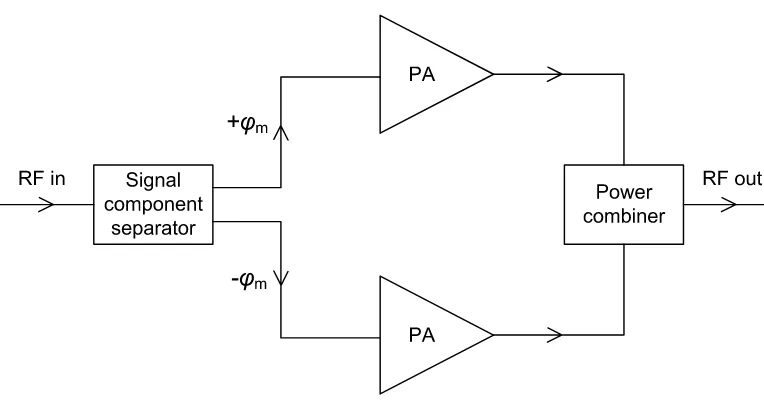
applied from HF [18] to microwave frequencies [19]. The signal component separator
performs AM-to-PM modulation to the RF input signal and generates two constant-envelope
signals with outphase relationships to each other. Two switching-mode amplifiers are used to
amplify each of the outphasing signals with high efficiency. By combining two
phase-modulated output signals from the amplifiers, the amplitude component of RF input is
14
Figure 2.3: Simplified envelope elimination and restoration (EER) system.
[image:34.612.160.502.119.334.2] [image:34.612.138.520.441.641.2]15
2.1.3
Output Power
The required output power of amplifiers is determined entirely by the aimed
applications. It ranges from several dBm for wireless handsets to hundreds of kilowatts for
ISM applications. For example, GSM handsets for 900 MHz require up to 2 W peak output
power, while RF power generators for induction heating need from 100 W to 100 kW at ISM
bands such as 13.56, 27.12, 900−930, 2450 MHz, etc.
In the case of communication systems with complex modulation schemes such as
CDMA, the output power varies dynamically following the modulated input signal. Then,
peak envelope power (PEP) is defined by instantaneous output power when the RF output
signal reaches its maximum swing. On the other hand, average power is calculated as the
time average of the instantaneous output power. The ratio between them, called
peak-to-average power ratio, is an important parameter in envelope analysis of linear power
amplifiers. However, in switching-mode amplifiers, output power commonly refers to the
peak envelope power because the input drive, in most applications, is fixed to make the
amplifiers operate in PEP condition. Sometimes, the output power is specified and measured
under two different conditions: continuous wave (CW) and pulsed operating conditions,
depending on applications. For example, most radar applications or some ISM applications
including plasma generation need pulsed operation rather than CW. Output power level along
with efficiency determines the amount of power that has to be extracted out of the operating
amplifiers by heatsink. Pulsed operation obviously puts less stringent requirements on the
heatsink. If duty cycle and efficiency in pulsed operation are D and η,respectively, then the
dissipated power that should be extracted by heatsink is
pulsed out, pulsed diss, 1 1 P D P ⎟⎟ ⎠ ⎞ ⎜⎜ ⎝ ⎛ − ⋅ =
η , (2.10)
where Pout,pulsed is the output power in pulsed operation. When D approaches unity, it
16
Output power has a trade-off with operating frequency mainly due to the limitation of
solid-state device technology. This is why vacuum-tube devices including klystron,
magnetron, and traveling wave tubes are still used to generate very high output power (up to
tens of MW) at high frequency (up to 100 GHz or higher). However, due to the innovative
advance of power transistor technology, solid-state power amplifiers are recently replacing
vacuum-tube devices up to around the 5 kW output power level. Efficient power-combining
techniques are essential to achieve such high output power with high efficiency, because the
maximum power that a single solid-state device can generate is still limited to hundreds of
watts even at HF/VHF frequencies [20].
2.1.4
Operating Frequency
Historically, switching-mode amplifiers have been proposed and demonstrated at low
frequencies (HF and lower) [7], [8], [21]. This is not only because of the frequency limitation
of active devices, but also because of the inherent operating mechanism of each
switching-mode that confines its application to low frequency. In particular, classic design
equations for Class-D [22] and Class-E [23] have been derived on the assumption of lumped
circuit elements. Those equations are fully valid at HF/VHF frequencies to obtain decent
switching-mode operations. However, as operating frequency goes up, it is hard to achieve
normal switching-mode operations and resulting high efficiency only with the equations, due
to distributed characteristics of circuit elements, limited switching speed of transistors, and
increased susceptance of drain-shunt capacitance.
Recently, several switching-mode amplifiers have been demonstrated at UHF and
microwave frequencies as a result of modification of design equations and transistor
technology improvements. Transmission-line Class-E amplifiers were demonstrated at
frequency as high as X-band [16], [24]. Class-D operation, which has been traditionally used
at very low frequency such as audio frequency, was adapted to build a UHF high-efficiency
17
switching-modes rather than in the ideal modes, the drain efficiency is still much higher than
any other transconductance amplifiers, reaching even 80 % at X-band [24]. Nonetheless, it
should be noted that efficiency and gain are generally degraded as operating frequency
increases.
2.1.5
Gain and Bandwidth
Gain of power amplifiers, defined in equation (2.5), have not been of primary concern
for most switching-mode amplifiers. The amplifiers have been designed at low frequency and
the inherent gain of transistors is very high at that frequency. In this case, power-added
efficiency becomes almost the same as drain efficiency, which, therefore, has been
exclusively used to measure the efficiency performance of the amplifiers. Also, in RF
generator applications, the most concerns are output power level and DC power consumption,
not the gain, because the input RF source is assumed to provide whatever amount of drive
power required for switching-mode operation. However, as operating frequency increases,
the gain drops rapidly and becomes one of the important criteria to be considered in
switching-mode amplifier design. The power-added efficiency also drops and shows a fair
difference from the drain efficiency. When the amplifier is used in a system, particularly in a
communication system, this power-added efficiency may be more important performance
than the drain efficiency. To compensate for the degraded gain and power-added efficiency,
preamplifiers can be employed before the power amplifier and generate sufficient input drive.
Bandwidth of amplifiers can be defined in different ways. For small-signal linear
amplifiers, it is usually defined as the width between two frequencies where the gain drops by
3 dB from its peak value. Although this definition can also be used for switching-mode power
amplifiers, the more widely used bandwidth is the one defined by output power, as shown in
Figure 2.5. Bandwidth that fulfills a certain level of efficiency is usually used for
18
Figure 2.5: Definition of bandwidth in terms of output power.
Intrinsically, switching-mode amplifiers have more or less narrow bandwidth. Resonant
tanks at the fundamental frequency and (or) harmonics are required in the output circuitry in
order to shape output voltage and current waveforms in switching-modes, which limits the
frequency response of the amplifiers. It is difficult to implement those resonant tanks that
present the appropriate impedance at each harmonic for wide range of drive frequency. To
overcome the constraint of narrow bandwidth, several techniques have been demonstrated,
including multi-band [26] and broadband [27], [28] switching-mode amplifiers.
2.2
Operating Classes of Power Amplifiers
Switching-mode power amplifiers are implemented in several different ways. Including
transconductance amplifiers altogether, there exist numerous types of power amplifiers that
have been proposed up to now. The most classical way to classify power amplifiers is to
designate each type as Class-A, AB, B, C, D, E, F [22], and so on. This classification is based
on DC bias condition, conduction angle, output terminations at fundamental and harmonics,
etc. However, it should be noted that the classification is somewhat ambiguous, so that an
amplifier could fall into two or more classes. Sometimes, one class may converge to another
19
The operating classes can be categorized into two broad categories for convenience.
Classes-A, AB, B, and C are categorized as transconductance amplifiers. Switching-mode
amplifiers refer to Class-D, E, and F. This section discusses basic operation theory of each
class.
2.2.1
Transconductance Amplifiers
In transconductance amplifiers, the transistor operates as a voltage-controlled current
source, as in a traditional way. Each different class is determined based on the conduction
angle, which is defined as a portion out of one whole period (2π) when the transistor conducts
non-zero drain current. Designers can choose different conduction angles from 0 to 2π and
the corresponding classes, by changing bias voltages and input-drive power.
2.2.1.1 Class-A
The bias point for Class-A amplifiers is located in the middle of I-V characteristics of the
transistor, shown in Figure 2.6. For the peak power operating condition, the DC voltage is
biased at the middle point between the knee voltage Vknee (in case of FET) and maximum
allowable voltage Vmax of the transistor. Also, the DC current is biased at the middle between
zero and maximum allowable current Imax. In this way, the load line of the amplifier becomes
straight centered at the bias point. The typical drain voltage and current waveforms are shown
in Figure 2.7. Note that the transistor conducts drain current all the time, which means the
conduction angle is 2π.
Since the Class-A amplifiers are always operated in the transconductance region (neither
the triode nor the cut-off region) as shown in Figure 2.6, the output current (or output
voltage) should follow the same waveform as the input voltage with minimum distortion.
This indicates the strong aspect of the Class-A amplifiers, which is high linearity. However,
the most serious drawback of the Class-A operation is low efficiency. Due to the DC bias
20
presented simultaneously. It generates huge power dissipation in the transistor, not in the
output load. Actually, the maximum allowable drain efficiency of Class-A amplifiers is
calculated only as 50 % [4]. This low efficiency limits the application of the Class-A
operation to low-power driver amplifiers or the amplifiers that require extremely high
linearity.
Figure 2.6: Bias points and load lines of transconductance amplifiers.
[image:40.612.229.425.509.674.2]21
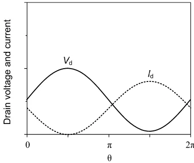
2.2.1.2 Class-B, AB
The gate bias in Class-B amplifiers is located at the threshold voltage of the transistor,
while the drain bias is similar to that of Class-A amplifiers, as shown in Figure 2.6. Thus,
when the transistor is driven by sinusoidal input, it is turned on for half of the drive time. For
the other half of the time, the transistor is turned off and the load line follows the zero-current
section. Consequently, the conduction angle of Class-B amplifiers is π, and the drain current
waveform becomes a half-sinusoid, as shown in Figure 2.8. The maximum drain efficiency
achieved at the peak envelope power condition reaches 78.5 %. Class-B amplifiers are
usually configured as a push-pull pair, which combines half-sinusoids from each amplifier,
operated 180° out-of-phase, and produces a full sine waveform in the output.
Class-AB is another common operating class used for linear amplification. The bias
point for Class-AB is located between Class-A and B. Thus the conduction angle is between
π and 2π, and the maximum drain efficiency is between 50 % and 78.5 %. Due to the
compromised characteristics of fairly high efficiency and linearity, this operating class is
widely employed for amplifiers in communication applications.
[image:41.612.229.425.478.644.2]22
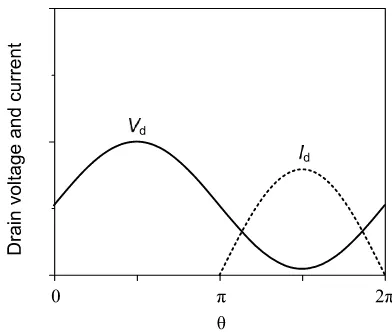
2.2.1.3 Class-C
The gate bias for Class-C is located below the threshold voltage, so that the conduction
angle becomes less than π. Figure 2.9 shows the drain voltage and current waveforms of
typical Class-C amplifiers. The current waveform is distorted from the sinusoidal or
half-sinusoidal one in Class-A or B, which degrades the linearity severely. At the expense of
low linearity, however, the Class-C amplifiers can achieve high efficiency, typically 75–80 %.
The drain efficiency increases as the conduction angle decreases, and it can achieve 100 %
drain efficiency in principle when the conduction angle becomes zero. Unfortunately, this
operating condition is not practical because the output power also becomes zero with a zero
conduction angle. Due to the high efficiency, the Class-C is widely used in high-power
amplifiers for CW and FM transmitter applications.
Figure 2.9: Drain voltage and current waveforms of ideal Class-C amplifiers.
2.2.2
Switching-Mode Amplifiers
In switching-mode amplifiers, the transistor is driven by a very large input signal, so that
the transistor operates as a switch rather than a current source unlike transconductance
[image:42.612.229.425.383.550.2]23
efficiency and high output power simultaneously. By minimizing the overlapping of non-zero
drain voltage and non-zero drain current waveforms, power loss in transistors is significantly
reduced, which means the increase of efficiency. In principle, the drain efficiency of
switching-mode amplifiers can be up to 100 % without output power degradation. Although
many loss mechanisms, such as ohmic loss and discharge loss, degrade the efficiency from
100 % in the real world, they still achieve above 90 % at HF [7], 80 % at VHF [29], and 70 %
at UHF and microwave frequencies [24], [25], [30], [31]. On the other hand, the linearity of
switching-mode amplifiers is very poor, because the output power is not a function of the
input power during the ideal switching operations. The input drive controls only the on-off
operation of the transistor, not the level of the output power. Therefore, switching-mode
amplifiers are commonly employed for CW operation or constant-envelope modulation
schemes that require less linearity. In order to improve the linearity of switching-mode
amplifiers, several system approaches have been proposed like EER and LINC, which are
described in Section 2.1.2.
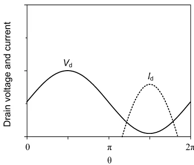
2.2.2.1 Class-D
Class-D uses two transistors that are usually driven in push-pull, so that they are
alternatively switched on and off. By this two-pole switching operation of transistors, the
drain voltage (in voltage-mode Class-D) or drain current (in current-mode Class-D) is shaped
to a rectangular waveform [4]. The output circuitry contains a bandpass filter that generates
sinusoidal output from the rectangular waveform of the drain terminal. Ideal drain voltage
and current waveforms are shown in Figure 2.10. Since there is no overlapping between drain
voltage and current waveforms, it can achieve 100 % drain efficiency. However, practical
Class-D amplifiers suffer from discharge loss generated in transistor output capacitance.
When the switch (that is, the transistor) is turned on, the charge stored in the transistor output
capacitance is discharged instantaneously through the on-switch. The amount of power loss
24
f V C
P 2
dc out
loss =2 , (2.11)
where Cout, Vdc, and f are transistor output capacitance, DC supply voltage, and operating
frequency, respectively. As can be seen in equation (2.11), the power loss increases with high
supply voltage and high frequency. This is why the Class-D is rarely used for the power
[image:44.612.230.425.262.428.2]amplifiers at high frequencies above VHF.
Figure 2.10: Drain voltage and current waveforms of ideal Class-D amplifiers.
2.2.2.2 Class-E
Class-E is one of the most popular switching-mode operations due to its high efficiency
characteristic and very simple circuitry as well. Usually, a single transistor is employed as a
switch and single-ended output is taken, although push-pull operation is also possible [23].
The basic schematic of the Class-E amplifier is shown in Figure 2.11. The transistor operates
as an ideal switch, but practically it includes small on-resistance and output capacitance
(represented by Cout). The externally connected shunt capacitance Cp is charged and
discharged along with the transistor output capacitance following the RF cycle and shapes the
drain voltage and current waveforms to fulfill the optimum Class-E operation. When the
25
current Id. When the switch is on, the current rises smoothly with no voltage across the
capacitors. The drain voltage and current waveforms for ideal Class-E operation are shown
in Figure 2.12. By avoiding the overlapping of voltage and current, it can achieve 100 %
drain efficiency ideally. The series resonant tank operates close to the input-drive frequency
f0, so that the harmonics are filtered out and the output voltage Vo becomes sinusoidal. The
important point regarding this resonant tank is that it should be designed in such a way that
the resonant frequency is a little off from the exact input-drive frequency. Actually, a small
amount of additional inductance (called detuning inductance Ldetuning) is required, which
makes the resonant frequency a little lower than f0. That is,
detuning res
0 L L
L = + , (2.12)
where Lres is the inductance to make a resonance exactly at f0 with C0:
0 res 0 2 1 C L f π
= . (2.13)
The detuning inductance makes the drain voltage fall to zero value with zero slope with
respect to time, at the time when the switch is turned on. These conditions are called ZVS
(zero voltage switching) and ZdVS (zero-voltage slope switching), which play significant
roles in eliminating discharge loss from the shunt capacitors Cout and Cp.
Assuming the optimum operating conditions that the voltage waveform satisfies the ZVS
and ZdVS and the duty cycle of input drive is 0.5, the following design equations are
derived [4]: L 0 out p 2 1836 . 0 R f C C π =
+ , (2.14)
0 L detuning 2 1525 . 1 f R L π
26
where R