HP Series 200 Computers
HP 98630
Breadboard Interface
Installation and Programming
Fliga
HEWLETT
Warranty Statement
The HP 98630 Breadboard Interface is warranted against defects in materials and workmanship for a period of ninety
(90) days. If HP receives notice of such defects during the
warranty period, HP shall, at its option, either repair or replace the defective product.
If the customer or any third party adds to or modifies the
HP
98630
Breadboard Interface
Installation and Programming
Manual Part No. 98630-90000
© CopYright Hewlett-Packard Company, 1983
This document refers to propnetary computer software which IS protected by copynght All rights are reserved COPYing or other reproduction of this program except for archival purposes IS prohibited without the pnor written consent of Hewlett-Packard Company.
Hewlett-Packard Desktop Computer Division
Printing History
New editions of this manual will incorporate all material updated since the previous edition. Update packages may be issued between editions and contain replacement and additional pages to be merged into the manual by the user. Each updated page will be indicated by a revision date at the bottom of the page. A vertical bar in the margin indicates the changes on each page. Note that pages which are rearranged due to changes on a previous page are not considered revised.
The manual printing date and part number indicate its current edition. The printing date changes when a new edition is printed. (Minor corrections and updates which are incorporated at reprint do not cause the date to change.) The manual part number changes when extensive technical changes are incorporated.
Table of Contents
Chapter 1
General Description
Applications Supported ... , . . . .
Wha t Thi s Manual Con tain s . . . 2
Where to Begin... . . . . . .. 2
Chapter 2 Mechanical Description The Breadboard Card.... . . . . . 3
Card Cages. . . . 5
Types of Cards and Card Placement . . . 6
I/O Card Coverplate.... ... . .. .... .. . . .. . . . .. .. .... .. .. .. ... .. ... . .. . ... . .. 7
Grounding. . . . . . .. 8
Installation. . . .. 9
Chapter 3 Theory of Operation Brief Overview . . . 11
Data Transfers . . . 12
Address Decoding. . . . .. 12
Data Direction and Upper/Lower Data Strobes Data-Transfer Acknowledgement. . . . .. 13
Register Access . . . 14
Interrupts. . . . . . . . . .. 16
Gene ral In te r rupt Timing . . . - . . . .. 16
Direct Memory Access . . . 17
Signal Loading... 17
Schematic Diagram and Parts List... 18
Chapter 4 Programming Notes Relevant Documentation . . . 20
BASIC . . . 20
Pascal. . . .. 20
Assembler Language... 21
Select Codes . . . 21
Interface Reset . . . 22
I/O Memory/Register Addresses . . . 23
External I/O Memory Map . . . 23
Standard I/O Registers . . . 25
Data Transfers . . . 28
Chapter 1
General Description
The HP 98630 Breadboard Interface allows experienced hardware designers to design custom interfaces. The interface consists of a printed-circuit (PC) board with a minimum of buffer components. These buffers connect user-supplied circuits to HP Series 200 Computers through the computers' backplanes.
There are approximately 15 square inches of unused space on the board intended for use as a prototyping area. This area, which is tinned for easy soldering, has a hole pattern on 1 DO-mil centers for conventional integrated-circuit (IC) packages as well as discrete components.
Applications Supported
The Breadboard Interface provides circuitry provides access to many of the signals on the Series 200 Computer backplane. The circuitry provided by this interface can be used in the following applications:
• data -transfer of bytes and words to and from peripheral devices
• memory registers on the board
• control lines to peripheral devices, and status lines from peripherals
• interrupt requests and acknowledgement
What This Manual Contains
This manual shows how to use the supplied components and unused space for your own circuits. The rest of this manual consists of the following chapters:
• Chapter 2 describes the interface from a mechanical standpoint. The dimensions of both PC board and rear-panel coverplate are given. Connector dimensions and vertical clearance are also provided.
• Chapter 3 describes how the interface works with HP Series 200 backplane signals. As you read this chapter, keep in mind that the signals on the backplane are fully discussed in the
11010 Bus" chapter of the Pascal System Internals Documentation, part number
09826-90074. A copy of the chapter is included with this documentation .
• Chapter 4 describes programming the Breadboard Interface in BASIC, Pascal, and MC68000 Assembler language.
Where to Begin
Before attempting to put any circuits on the PC board, you should become familiar with the physical layout of the interface, how it operates, and specific requirements of any circuitry you add to the board. Read Chapters 2 and 3 for this information.
The 010 Bus chapter fully discusses the Series 200 backplane signals; you will definitely need to refer to that document while reading this manual. You may also want to refer to the MC68000 User's Manual, HP part number 09826-90073, for a description of the MC68000 microprocessor signals and operation.
After you are generally familiar with the interface and how it operates, you can begin to formulate and implement design ideas. Chapter 4 provides suggestions for programming the interface.
Chapter 2
Mechanical Description
This chapter describes the mechanical characteristics of the Breadboard Interface. Drawings of the interface card, the card cage into which it plugs, and rear-panel cover plate are given.
The Breadboard Card
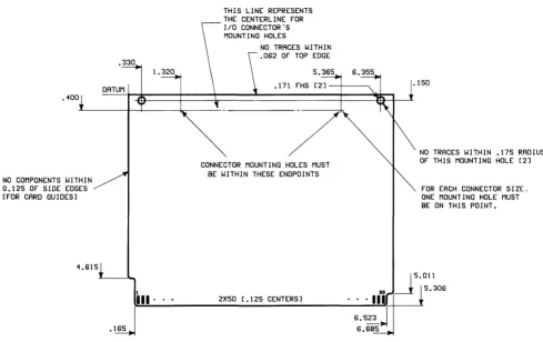
The Breadboard Interface's printed -circuit (PC) board, or card, is the same size as other input/output (I/O) cards. The following drawing shows the dimensions required of all I/O cards, as seen from the component side of the card.
.400
NO COMPONENTS WITHIN
0.125 OF SIDE EDGES [FOR CARD GUIDES]
.330
DATUM
THIS LINE REPRESENTS THE CENTERLINE FOR I/O CONNECTOR'S MOUNTING HOLES
NO TRACES WITH I N
.062 OF TOP EDGE
5.365 6.355 .171
/
CONNECTOR MOUNTING HOLES MUST BE WITHIN THESE ENDPOINTS
.150
NO TRACES WITHIN .175 RADIUS OF THIS MOUNTING HOLE [2]
FOR EACH CONNECTOR SIZE, ONE MOUNTING HOLE MUST BE ON THIS POINT.
~~ ___________ 2X_5_0_[_._1_25 __ C_EN_T_ER_S_] ________ ' __ '~' III
~
U5'~1'~06
6.5~J
6.685
Blank I/O Card
The following drawing shows the component side of a Breadboard Interface card with relevant dimensions. At the rear of the card are pre-drilled, plated-through holes into which the pins of a connector may be inserted. One mounting hole for the connector has also been drilled in the card. The position of the second mounting hole depends on the size of connector you will use.
CENTERLl NE FOR I/O CONNECTOR'S MOUNTING HOLES
TOOLI NG HOLE
GROUND BUS [+5V POWER BUS ON
CIRCUIT SIDE]
TOOLING HOLE
CONNECTOR MOUNTING HOLES MUST BE WITHIN THESE ENDPOINTS
5.365 6.355
.150
h=================================~~====;\1 ~
TOOLING HOLEI
PROTOTYPING AREA [6.1 IN. X 2.5 IN.] CONTAINS 62 HOLES BY 26 HOLES
ON 0.1 INCH CENTERS
3800000 •
I 00000 • : ~~~~~ ~~ Pl [70 PINS]
c:=J .
c:=J.
. c:=J
. c:=J
III· .. P2 [2X50 [.125 CENTERS]]
The Br.eadboard Interface Card
MOUNTING HOLE FOR REAR PANEL
FOR EACH CONNECTOR SIZE, ONE MOUNTING HOLE MUST BE ON THIS POINT.
IC'S [Ul THRU U12]
You can place prototype (or final) circuits on the center portion of the card. This area consists of a matrix of holes on O.l-inch centers, which will accomodate standard integrated-circuit (IC) packages and sockets. There is a ground plane on the component side of the card and a power
plane (+ 5 volts) on the circuit side. Supply voltages of + 12 and -12 volts are also available. See
Chapter 3, "Theory of Operation," for further details.
Card Cages
Series 200 optional interface and memory cards reside in a card cage which is entirely within the computer (or expander) case. The cards, positioned with the aid of card guides, plug into connectors on a common backplane which contains the system's Desktop-computer Input/Output (DIO) Bus.
The HP 9826/9836 Card Cage
Types of Cards and Card Placement
There are two types of option cards: interface (or I/O) cards and non-I/O cards. I/O cards are designated as such because they communicate with peripheral devices through a cable connected to the card's coverplate. Non -I/O cards do not communicate with peripheral devices. Non -I/O cards include such types as memory and Direct Memory Access (DMA) Controller cards.
The size and placement of the coverplate on an I/O card is such I/O cards can only be inserted in every other slot in the card cage, beginning with the bottom slot (see preceding drawing). The coverplate covers the I/O card and the non -I/O card above it.
1/0
Card Coverplate
The following drawing shows the dimensions of the blank coverplate supplied with the HP 98630. The drawing shows the placement of different sizes of connectors which can be used with the Breadboard Interface.
1.6 FULL R 1.6R (4)
107.8 122.9
~I~ ~~cr---~~
8.82 138.16.5 12.8(2)*
1.6R (2)
C'SINK 6.86 DIA X 90° (2) 3.2R(4)
I/O Card Coverplate
The drawing shows cut-outs and drilled holes for 24-, 36-, 50-, and 64-pin connectors. Amphenol manufactures connectors which can be used with the Breadboard Interface, as shown in the following table.
Connector Size
24-pin 50-pin 64-pin
Amphenol Part Number
57-92245-12 57-92505-12 57-92645-12
Grounding
In order to ensure safe, reliable operation with Series 200 Computer products, all specifications
in this document must be strictly followed when designing Bus Slave devices. Keep in mind that
you are responsible for any circuitry that you design and use with HP products, both in terms of
personal safety and proper operation with the equipment.
I/O cards must be designed to meet all UL, CSA, and IEC safety requirements. The connector
(both shell and pins) and I/O cable must be grounded through the rear coverplate, which is electrically and mechanically connected to the chassis through the dog-bolts which secure the card in the card cage. This grounding scheme must meet the following requirements:
1. Ground -current carrying capacity: The conductive path between the I/O cable (cable shield, connector ground pins, and connector shell) and the safety ground pin of the power receptacle must be capable of carrying 30 amperes for 120 seconds. This requirement can be expressed in ohmic resistance for the following two cases:
a. For cable lengths less than 4 metres, the dc resistance between the end of the cable and the safety ground pin of the power receptacle should be less than 100 milliohms.
b. For cable lengths greater than 4 metres, the dc resistance between the I/O connector on the card's coverplate (cable shield, connector ground pins, and connector shell) and the safety ground pin of the power receptacle should be less than 100 milliohms.
WARNING
I/O CABLES AND CONNECTORS WHICH ARE NOT GROUNDED AS STATED ABOVE PRESENT A POTENTIAL SHOCK HAZARD TO THE USER OF THE EQUIPMENT.
2. Fault-current carrying capacity: A UL/CSA/IEC requirement is that any device operating from a supply capable of supplying more than 8 amps be fused. Therefore, any board
plugged into the backplane must have a 4-amp maximum fuse in series with the + 5V bus.
CAUTION
Installation
Use the following procedure to install interface card(s) in the computer.
1. Turn computer power off. If the interface is connected to a peripheral, disconnect it from
the peripheral.
CAUTION
BEFORE INSTALLING ANY INTERFACE IN THE
COMPUTER, BE SURE THAT POWER IS OFF. FAILURE TO DO SO MAY DAMAGE THE COMPUTER, VOIDING ANY WARRANTY IN EFFECT.
2. Slide the card into one of the slots in the card cage. Remember that I/O boards will only fit in every other slot, beginning with the lowest slot, because of the coverplate.
3. Make sure that the edge of the card is aligned properly with the backplane connector, and
then tighten the dog bolts finger tight. This is a very important step, since these bolts secure
the card in the cage and provide a path to the ground terminal of the computer's power cord.
4. Connect the I/O cable to the coverplate.
Chapter 3
Theory of Operation
This chapter describes the signals provided by the Breadboard Interface. A block diagram shows the different parts of the circuits provided with the board. A brief description of operation describes how the circuits operate. A complete schematic diagram shows circuit components, signal names, and connector pins.
Brief Overview
The Series 200 Computer backplane is an implementation of the Desktop-computer I/O (DIO) Bus. The DIO Bus is basically an electronically buffered version of the asynchronous input and output (I/O) bus of the MC68000 microprocessor. You may want to refer to the MC68000 User's Manual, HP part number 09826-90073, as you read this discussion.
Note
Keep in mind that the timing information given in the DIO Bus chapter refers to the signals at the inputs of the drivers on the Processor Board. The signals that arrive at the backplane may already have been skewed by variations in the 74LS245 buffer devices on the processor board and capacitances of the bus lines. See "Bus Timing Background" in the first section of the DIO Bus chapter for a diagram showing the originations of bus skew.
The Breadboard Interface can be used to implement three general types of I/O operations:
• data transfers
• interrupt requests and acknowledgements
• direct-memory access (DMA) operations
Data Transfers
The data-transfer portion of the interface consists of address-decoding and data-bus management circuits. The standard interface registers on the board are considered part of this circuitry. See Chapter 4 for the standard interface registers' offset addresses and definitions.
Address Decoding
The twenty-three Buffered Address lines of the backplane (BA23 through BAt) are available to the Breadboard Interface. The most significant eight bits (BA23 through BA 16) are used to select the interfaces and are not accessible to the circuitry added to the board. The following block diagram shows this portion of the circuitry.
Buffered Address Lines
AIO Bus Lines (Computer Backplane)
I'm Addressed (IMA)
Buffered Address Strobe (BAS)
(BA23 thru BA 16)
(BA15 thru BA1)
Breadboard Interface Circuitry
Address Comparison
(A15 thru A1)
User-Supplied Circuits
+5V1
Select Code Inputs
The address-decoding circuit consists of a digital comparator (V 11) which compares the address placed on the address bus to the address setting of the interface (SC4 through SCO). The three most significant bits of the interface's address setting (which are compared to BA23 through BA21) are hard-wired to "OIl," respectively. The next five bits (which are compared to BA20 through BA 16) are determined by the logic levels placed on SC4 through SCO, respectively. These five signals are used to set the interface to select codes 0 through 31.
The select code can be set by tying the ,signals called SC4 through SCO either to logic High (to match a "1" on that address bit) or logic Low (for a "Oil). For instance, the interface is assigned a select code of 31 when all lines are tied High.
Note that the interfaces occupy computer memory space from hexadecimal addresses 600 000 to 7FF FFF. This space is divided into thirty-two equal sections by BA20 through BA 16, each of which occupies 65 536 (hexadecimal F FFF) memory addresses. Each interface can potentially have this number of memory locations.
During access cycles, the address is placed on BA23 through BA 1 and allowed to settle (for at least IS nanoseconds) before Buffered Address Strobe (BAS*) is asserted (Low). On the Breadboard Interface, this strobe enables the comparison of the address to the select code (pin 1 of V11).
The interface detects that it is addressed when the comparator (V 11) asserts its IIP=Q" output (pin
19), which gates the I'm Addressed signal (IMA *, pin 3 of V 1) onto the backplane. This response
is automatically made by hardware on the interface in the required 40-nanosecond response time.
The interface (or peripheral) must complete the transaction by acknowledging with the Data Transfer Acknowledge signal (DTACK*, pin 6 of V 1), as described in the next section.
Data Direction and Upper/Lower Data Strobes
The DIO Bus defines the direction of the data with the Buffered Read/Write signal (BR/W*, pin
11 of V9). When BR/W* is negated (logic High), the Bus Master (processor board) is reading data
from the card; when BR/W* is asserted (logic Low), the master is writing data to the card.
The bus also defines which of the data lines are to be used in the transfer: Buffered Vpper Data
Strobe (BVDS*, pin 13 of V9) indicates that the upper data byte (DIS through D8) is to be used,
while Buffered Lower Data Strobe (BLDS*, pin 1 7 of V9) indicates that the lower byte (D7
through DO) is to be used. If both are asserted (Low), then all 16 data lines are to be used in the transfer.
These data strobes are directly from the processor board. There are also two other available data
strobe signals (VDCS* and LDCS*) which are qualified by Card Select (CS*).
Data -Transfer Acknowledgement
The acknowledgement on DTACK* (made by the interface or peripheral device) must get back to the processor within 3.0 microseconds of BAS* being asserted.
During read operations, this acknowledgement indicates that the interface has placed the data on the appropriate data lines and that the data can be read. During write operations, it indicates
that the data have been accepted by the interface. If this acknowledgement is not made within 3
General Data -Transfer Timing
For data transfer, the general I/O protocol is as follows. Refer to the Breadboard schematic diagram as you read through this description. Details of data -transfer timing are fully discussed in the DIO Bus chapter.
1. The R/W* signal is used to indicate data direction (High=Read from interface, Low=Write to interface)
2. The address is placed on A 23 thru A 1
3. The Buffered Address Strobe (BAS*) is asserted to indicate that the address is valid
4. If A23 thru A21 are "01111
and A20 thru A16 match the select code switches, the card recognizes that it is selected
5. The Card Select signal (CS*) is generated by Breadboard Interface hardware
6. The CS* signal asserts the I'm Addressed signal (IMA*), which signals that an interface is present at that select code
7. The Vpper Data Strobe (VDS*) and/or Lower Data Strobe (LDS*) are asserted to indicate which data lines (D15 thru D8 and/or D7 thru DO, respectively) are to be used in the transfer
8. The data are read or written (after settling)
9. The CS* signal has already enabled the DTACK* buffer (VI pin 4) to drive the DTACK* line on the bus (V I pin 6) with the current logic level of DTACK* on the card (V 1 pin 5)
10. When DT ACK* is detected within 3 microseconds, the data transfer is complete. If it is not detected within this time interval, a bus error occurs. See the DIO Bus chapter for further details on bus error processing.
Register Access
The Breadboard Interface has four built-in registers: Read Registers I and 3, and Write Registers 1 and 3. These are standard interface registers whose definitions are given in the DIO Bus chapter and in Chapter 4 of this manual.
UDCS* LDCS*
Address Lines
Register
(See Note 1)
15 14
. 2 1
Selected
o
0 X X X X X X X X X X 0 0
Register
o
0 X X X X X X X X X X 0
Register 3
o
0 X X X X X X X X X X 1 0
Register 5
o
0 X X X X X X X X X X 1 1
Register
7X 1 X X X X X X X X X X X X
8Kbytes
o
X X X X X X X X X X X X
8Kbytes
1 X X X X X X X X X X X X
8Kbytes
X X X X X X X X X X X X X X
32 Kbytes
Notes
1. Note that no entry exists in one of the UDCS* and LDCS* columns while the other shows a "1." This convention indicates that the table shows the addresses of bytes, not words. Showing these signals asserted at the same time would obscure the information shown in the table.
Interrupts
The interface accepts interrupt requests from external source(s), or from sources added to the board. These interrupts can be given one of four different hardware priorities. Hardware provided on the Breadboard Interface takes care of generating an interrupt request on the appropriate hardware interrupt level. The program can assign a software. priority to the interrupt's service routine.
The following diagram describes the interrupt circuitry provided with the Breadboard Interface.
AIO Bus Lines (Computer Backplane)
Interrupt Level (IL3 thru IL6)
General Interrupt Timing
Breadboard Interface Circuitry
1-of-4 Decoder
Interrupt Circuitry
User-Supplied Circuits
} Interrupt Level Inputs
From Interrupt Enable Register (Built-In)
From User-Supplied Circuit or Peripheral Device
The general interrupt request and acknowledge cycle is as follows:
1. The Breadboard Interface or an external peripheral asserts the Interrupt Request signal (IR, pin 6 of PO
2. If interrupts are enabled (IE, pin 8 of U4, is High), the outputs of the l-of-4 decoder (U8) are enabled. Decoder inputs IL 1 and ILO (pins 3 and 13 of U 8, respectively) determine which output is asserted (Low).
3. It is then up to the language system to process the interrupt properly. Programming interrupt service routines is discussed in Chapter 4.
Note
Externally vectored interrupts are not supported with the DIO Bus.
Direct Memory Access
The Breadboard Interface has no built-in circuitry for handling DMA applications. All DMA applications must be implemented by your own circuit designs. See the DIO Bus chapter for a complete description of DMA operations.
Signal Loading
The DIO Bus chapter provides the loads which can be each placed on each backplane signal. You can use these figures for backplane signals which are not buffered by the Breadboard Interface (such as DMARO*, DMAR1*, and BA13 -- BA3).
Schematic Diagram and Parts List
The schematic diagram and component locator of the HP 98630 Breadboard Interface are located at the rear of this manual.
This is the list of components supplied with the 98630 interface.
Component Device
Designator Number Description
U1 74LS125 Quad 3-State Buffer
U2 74LS138 1-of-8 Decoder
U3 74LS32 Quad 2-Input Nor Gate U4,U5,U9 74LS244 Octal Buffer
U6,U12 74LS245 Octal Transceiver U7 74LSOO Quad 2-Input Nand Gate U8 74LS156 Dual 1-of-4 Decoder (OC)
U10 74LS273 8-Bit Register
Ull 74LS688 Octal Comparator
C1 0.1 uF Capacitor
C2 thru C7 O. 1 uF Capacitor (DIP)
R1 1.0 kOhm Resistor
F1 1 .5 A Fuse
Chapter 4
Programming Notes
This chapter provides brief notes regarding programming the Breadboard Interface using BASIC, Pascal, and MC68000 Assembler languages. Programming the card in HPL is very similar to BASIC.
The following topics are discussed in this chapter:
• Select codes
• Memory/register addresses
• Interface reset
• Data transfers
• Bus errors
• Interrupts
• DMA operations
Relevant Documentation
This section lists the manuals that you will need to consult to write programs for the Breadboard Interface, because actual techniques for programming the interface are only outlined in this manual.
BASIC
BASIC programming techniques for HP Series 200 interfaces are described in the following
manuals:
• BASIC Interfacing Techniques, part number 09826-90025 (or 09826-90020, which is an earlier edition)
• BASIC Language Reference, part number 09826-90056 (or 09826-90055, which is an earlier version).
The only directly relevant information regarding the Breadboard Interface is the brief discussion of the READIO and WRITEIO registers in Chapter 6 of BASIC Interfacing Techniques. However, you may want to read Chapters 8 through the end of the book to find out about how the other interfaces operate and are programmed to get some design ideas. The installation manuals for each interface may also provide valuable hardware-design ideas. Syntax and semantics for the READIO and WRITEIO keywords are described in the BASIC Language Reference.
Pascal
Pascal programming techniques applicable to the Breadboard Interface are described in the following manuals:
• Pascal 2.0 User's Manual, part number 98615-90020 (or the 09826-90070 for Pascal 1.0)
• Pascal Procedure Library User's Manual, part number 09826-90075
• Pascal System Internals Documentation, part number 09826-90074.
Assembler Language
Assembler language programming techniques applicable to the Breadboard Interface are described in the following manuals:
• Pascal 2.0 User's Manual, part number 98615-90020 (or the 09826-90070 for Pascal 1.0)
• MC68000 User's Manual, part number 09826-90073
The Assembler is accessed from the Pascal system as described in the Pascal User's Manual. The
MC68000 User's Manual describes Assembler language programming for the 68000 microprocessor. The Pascal manual describes Assembler directives.
Select Codes
The select code inputs (SC4 through SCO) can be used to set the card to select codes 0 through 31; however, only select codes 8 through 31 are usable with BASIC and Pascal, since these systems map select codes 0 through 7 into internal I/O devices. With Assembler language programs, all select code settings can be used; resultant base addresses are 600 000 through 7FO 000 (hexadecimal). Select codes and resultant addresses are further described in a subsequent section of this chapter.
Note
The select code used for this interface must not be used by any
other interface currently in the computer or in an HP 9888
Interface Reset
There are two ways to reset the Breadboard Interface: press the [RESET] key ([SHIFT] - [PAUSE]), or write to register 1. Pressing [RESET] pulses the RESET* and SRESET* signals low, while writing to register 1 pulses SRESET* only. Thus, the result of resetting the card depends on what you have connected to these signal lines; however, in general, Interface Reset should be a method of bringing a card to some known state.
The data written to register 1 is irrelevant -- the mere operation of writing to that register resets the card. Note also that the contents of register 3 (U 10 and bits 0 and 1 of U 4) are cleared.
With BASIC, use the WRITEIO statement to write to register 1. An example might be as follows:
Select_code=15 Register=1
Data=An_integer
WRITEIO Select_code,Register;Data
With Pascal, use the procedure called "iowrite_byte." An example Pascal statement, which analogous to the preceding BASIC-language WRITEIO statement, is as follows:
iowrite_byte(24,1,Anydata);
It is also suggested that you use the "ioinitialize" and "iouninitialize" procedures before and after performing I/O operations, respectively. Keep in mind that the program must IMPORT the GENERAL_O and GENERAL_1 modules to use these and the "iowrite_byte" procedures. See the Pascal procedure library manual for further details.
I/O Memory /Register Addresses
The Breadboard Interface implements all "standard" I/O registers. These registers are described later in this chapter.
The preceding section showed an example of writing into a register on the Breadboard Interface by using the WRITEIO statement. The first argument of the statement was the select code; the second was the register number (or "offset address" of the register, from the card's base address). The third argument was the integer data written into the register; this argument's INTEGER value is obtained and written into the register by the WRITEIO statement.
'''i
Similarly, registers can be written by using the READIO numeric function. An example is as follows.
Enable_reg=READIO(24,3)
The preceding statement reads the value of register 3 on the card at select code 24. The register's contents are placed in the numeric variable Enable_reg.
The preceding examples do not take into account whether or not the register is an eight- or sixteen-bit register. If the register being read is a sixteen-bit register, the data must be read with
two READIO statements: one READIO will be used to read the upper eight bits (which are at an even offset address), and another READIO will be used to read the lower eight bits (on the next-higher odd address). With Pascal and ~sembler languages, you can use procedures (or instructions) that access a word of data in one operation.
External I/O Memory Map
The External I/O address space is divided into 32 segments of 64 Kbytes each. The I/O cards contain select code switches which determine the physical address of the card in the External I/O address space. Five switches permit the user to choose one of 32 select codes, ranging from 0 through 31, to determine which 64 Kbyte address space the card resides in. Switches should be implemented in the I/O card design for flexibility reasons. The address format, shown below, locates I/O devices in memory locations 600 000 through 7FF FFF. Note that all registers or memory locations on an I/O card are offsets to the card's "base address."
Address Bit:
23 22 21 20 19 18 17 16 15 14 13 12 11 10 9 8 7 6 5 4 3 2
o
1 1o
0 0 0 0thru
1 1
Hard-wired Select Code Switches (0 thru 31)
Register Number (Offset to Base Address)
Registers (offsets) 0 thru 65535
SELECT BASE STANDARD CODE ADDRESS ASS I GJ\t.1ENT
7FFFFF 31 7FOOOO Reserved
30 7EOOOO Reserved
29 700000 98627 (continued) 28 7COOOO 98627 Color Output 27 7BOOOO Reserved
26 7AOOOO Reserved 25 790000 Reserved 24 780000 Reserved 23 770000 Reserved 22 760000 Reserved 21 750000 98629A SRM 20 740000 98628A Datacomm 19 730000 Reserved
18 720000 Reserved 17 710000 Reserved
16 700000 Custom I/O Card 2 15 6FOOOO Custom I/O Card 1 14 6EOOOO 98625 Disc
13 600000 Reserved 12 6COOOO 98622 GPIO 11 6BOOOO 98623 BCD 10 6AOOOO Reserved
9 690000 98626 RS-232 Note 1
8 680000 98624 Ext. HP-IB
- -
-
-
-
-
-
- -
- -
-
-
-7 670000 6 660000 5 650000 4 640000 3 630000 2 620000 1 610000 0 600000 600000
Standard 1/0 Registers
The standard I/O card registers are defined as follows; the register number is the offset (added to the base address of the card) which is used to access the register.
Read Register 1: ID Register
Bit 7 Bit 6 Bit 5 Bit 4 Bit 3 Bit 2 Bit 1 Bit 0
0 0 0 104 103 102 101 100
Value Value Value Value Value Value Value Value
=128 =64 =32 =16 =8 =4 =2 =1
ID4 thru IDC -- Contain the card ID, which uniquely identifies each type of I/O card.
Currently Defined 10 Numbers
0 - Reserved 16 - Custom I/O Card 2
1 - 98624 17 - Reserved
2 - 98626 18 - Reserved
3 - 98622 19 - Reserved
4 - 98623 20 - 98628A/98629A 5 - Reserved 21 - Reserved 6 - Reserved 22 - Reserved 7 - Reserved 23 - Reserved
8 - 98625 24 - Reserved
9 - Reserved 25 - Reserved 10 - Reserved 26 - Reserved
11 - Reserved 27 - Reserved 12 - Reserved 28 - 98627 13 - Reserved 29 - Reserved 14 - Reserved 30 - Reserved 15 - Custom I/O Card 31 - Reserved
Write Register 1: Interface Reset
I
Bit 7 Bit 6 Bit 5 Bit 4 Bit 3 Bit 2 Bit 1 Bit 0I
I
I
The value written into thisI
register is irrelevant.I
"I Value Value Value Value Value Value Value Value
I
=128 =64 =32 =16 =8 =4 =2 =1I
Writing any value into this register performs an Interface Reset of the card. The card's actual response to this action depends on how it is designed.
Good system design requires that the operating system should be capable of resetting an I/O card to its power-on state. One of two methods must be implemented:
1. If the card contains LSI chips, one or more commands may be defined which can be sent to gracefully return the card to its power-on state.
2. If the card does not have such a sequence, the card may be capable of being reset to its power-on state by writing to register 1.
Read Register 3: Interrupt and DMA Status
Bit 7 Bit 6 Bit 5 Bit 4 Bit 3 Bit 2 Bit 1 Bit 0
IE
IR
INT LVL Undefined DEl DEOSwitches
Value Value Value Value Value Value Value Value
=128 =64 =32 =16 =8 =4 =2 =1
IE -- Interrupts Enabled: If this bit is set, interrupts are enabled.
INT LVL Switches -- Interrupt Level: The interrupt level is typically set by two switches on the I/O card; these switches map into the 2 Interrupt Level bits.
Switch Setting
o
0o
11 0 1 1
Interrupt Level
3
4
5 6
Undefined -- These bits have no standard definition and are thus are available for user-defined functions.
DE 1 -- When this bit is set, DMA is enabled on channell.
DED -- When this bit is set, DMA is enabled on channel D.
Write Register 3: Interrupt and DMA Enable
Bit 7 Bit 6 Bit 5 Bit 4 Bit 3 Bit 2 Bit 1 Bit 0
EI Undefined DEl DEO
Value Value Value Value Value Value Value Value
=128 =64 =32
=
16 =8 =4 =2 =1EI -- Setting this bit enables interrupts.
Undefined -- These bits have no standard definition and are thus are available for user-defined functions.
DE 1 -- Setting this bit enables DMA operations on Channell.
Data Transfers
Data transfers are generally implemented with handshakes or some other similar synchronization method. Pascal and Assembler languages support DMA and interrupt operations for data transfer; interrupts and DMA operations are not possible with BASIC.
The BASIC-language OUTPUT, ENTER, and TRANSFER statements cannot be used with the Breadboard Interface, since the operating system cannot call firmware drivers for this card. This section briefly describes implementing a handshake.
Let's suppose that your Breadboard Interface has additional read and write registers which are available for general-purpose use. Let's also suppose that your peripheral device has the f ollowing four handshake lines:
• a Peripheral Status (output) line which indicates whether the peripheral is "OK" or "not OK"
• a Peripheral Control (input) line which it monitors as a "transmit request" from the computer
• a Data Direction (input) line which indicates whether the computer is to send or receive data
• a Peripheral Flag (output) line that indicates whether it is Ready or Not Ready to receive (or transmit) data
Let's, yes, even further assume that you just happen to have four registers on your Breadboard Interface, two of which can be read to determine the state of the two output lines from the peripheral and two of which can be written to set the two inputs to the peripheral. For simplicity, assume that bit 0 of all four registers is connected to the relevant signal line.
100 Select_code=15 110
120 ! Define register numbers.
130 Dir_reg=9 To define data direction. 140 Psts_reg=7 To read Peripheral Status line. 150 Data_reg=7 To write Data (8 bits).
160 Pflg_reg=5 To read Peripheral Flag line. 110 Pctl_reg=5 To write Peripheral Control line. 180 !
190 Data$="ASCII Characters" 200 !
210 Ok=READIO(Select_code,Psts_reg)
220 IF Ok THEN ! Peripheral is OK, so send data.
230 WRITEIO Select_code,Dir_reg;l ! Set direction=out. 240 FOR Char=1 TO lEN(Data$)
250 Ready_chk:Ready=READIO(Select_code,Pflg_reg) ! Check for PFlG=Ready. 260 IF NOT Ready THEN Ready_chk
270 WRITEIO Select_code,Pctl_reg;O Clear PCTl.
280 WRITEIO Select_code,Data_reg;NUM(Data$[Char;1]) Place byte.
290 WRITEIO Select_code,Pctl_reg;1 Set PCTl.
300 NEXT Char
310 ELSE ! Peripheral is NOT OK, so quit.
320 PRINT "Peripheral Error on select code";Select_code 330 END IF
340 !
350 END
Bus Errors
As shown in the Read and Write Cycle timing diagrams, the peripheral (or Breadboard Interface) must respond to the computer's request for a data transfer by asserting DT ACK* within the specified time. When this acknowledgement is not made, the Processor Board generates a "bus error.1I
The BASIC-language operating system reports Error 163 I/O interface not present. You can use ON ERROR to recover from the error, if desired. With Pascal, you may want to use TRY/RECOVER to process any errors encountered. With Assembler language, the processor handles the error as an "exceptionll
and uses exception vector number 2. See the MC68000 User's Manual for further details.
Interrupts and DMA Operations
The DIO Bus
Table
of Contents
Introduction... 1 Objectives... 1 Designer 1 s Responsibili ties. . . . . 1 Signal Terminology... 2 System Elements. . . . . . . . . .. 2 Bus Timing Background. . . . . . . . . . .. 4 Memory Map. . . . .. 6 Series 200 Memory Map. . . . .. 6 Registers. . . . . . .. 9 Data Transfers. . . .. 12 Data Transfer Signals. . . .. 12 Data Transfer Overview . . . 13 Read Cycle Description . . . 13 Wri te Cycle Description . . . 16 Read-Modify-Write . . . 19 Enable DTACK Timing. . . . .. 19 Direct Memory Access . . . 22 DMA Signal s. . . . . . .. 22 DMA Overview . . . 22 DMA Output Cycle Description . . . 23 DMA Input Cycle Desc ription. . . .. 25 DMA Speed Considerations . . . " 27 Terminating DMA Transfers . . . 28 Bus Error Operation . . . 29 The Bus Error Signal . . . 29 Bus Timeouts . . . 29 Interrupt Operation . . . 31
The 010 Bus
Introduction
The Series 200 Desktop-computer Input/Output (DIO) Bus standard defines both mechanical and electrical requirements of cards which are to be used as optional input/output (I/O) devices with HP Series 200 Computers. The DIO Bus was first implemented in the Model 26 Computer (HP 9826A), followed shortly thereafter by the Model 36 (9836A) and the Model 16 (9816A). The 9888A Bus Expander, which can be used with Series 200 Computers, also implements the DIO Bus.
The DIO Bus is designed around the MC68000 series of microprocessors. If you want further
information regarding MC68000 operation, refer to the MC68000 User's Manual, HP part
number 09826-90073.
Objectives
The purpose of this document is to provide sufficient documentation to permit experienced digital-hardware designers to develop devices for use with the DIO Bus. The goal is to provide enough information to design Bus Slaves -- in particular, I/O cards. Bus Masters, such as Processor and DMA Controller boards, cannot be designed by using the information in this document. You may want to use the HP 98630 Breadboard Interface as the beginning of your own custom interface.
Any questions you may have regarding the information in this document should be brought to the attention of your local HP Desktop Computer Systems Engineer.
Designer's Responsibilities
In order to ensure safe, reliable operation with Series 200 Computer products, the specifications in this document must be strictly followed when designing Bus Slave devices. The IIElectrical Specifications" and IIMechanical Specifications" sections describe topics such as available power-supply current and size requirements of I/O cards. The section called "Design Qualification" provides safety and operating requirements that your I/O card design must meet to qualify as a usable device.
CAUTION
HEWLETT-PACKARD SHALL NOT BE LIABLE FOR ERRORS CONTAINED HEREIN OR FOR INCIDENTAL OR CONSEQUENTIAL DAMAGES IN CONNECTION WITH THE FURNISHING, PERFORMANCE, OR USE OF THIS MA TERIAL. REP AIRS NECESSIT A TED BY MISUSE OF THE EQUIPMENT, OR BY HARDWARE, SOFTWARE, OR
INTERFACING NOT PROVIDED BY
HEWLETT-PACKARD ARE NOT COVERED BY THE WARRANTY.
Signal Terminology
The following convention is used throughout this document: Active-low signals are denoted with a * following the name. This is equivalent to a bar over the signal name which is often used for active-low signals. Thus, the following are equivalent:
BAS*
=
BAS
When a signal is referenced as "asserted" or "true," "negated" or IIfalse,1I and so forth, it is relative
to the signal's function. For example, to say that BAS is asserted means that it is active
(performing its function). Whether it exists as BAS (active-high) or BAS* (active-low) on the backplane is irrelevant.
References to IIhighll and IIlowll refer directly to TTL logic voltage levels. When referring to high and low signals, the actual name of the signal is used. For example, when the signal BAS* is described as being low, the signal entitled BAS* has a TTL logic-low voltage level. The TTL logic levels are defined as follows:
Logic High: >= 2.0 volts
Logic Low: <= 0.8 volts
System Elements
The functional modules of the 010 Bus are shown below. Where signals go specifically from one
--->
SA23
-
SAl
--->
--->
BAS*
--->
<---
IMA*
---SUS
--->
BR/W*
--->
BUS
--->
BUDS*
--->
MASTER
--->
BLDS*
--->
SLAVE
<--->
SD15
-
BOO
<--->
--->
ENDT*
--->
<---
DTACK*
<---Figure la. Data-Transfer System Elements
INTERRUPT
REQUEST
HANDLER
1 1 1<---1_ _ _ _ _ _ 1
1
1
IR3* - IR6*
---1
1
INTERRUPT
REQUESTER
1 _ _ _ _ _
-Figure lb. Interrupt System Elements
1
1<---1--->
DMA REQUEST
1HANDLER
1<---1--->
1
1<---1--->
_ _ _ _ _ _ 1
DMARO*
DMACKO*
DMAR1*
DMACK1*
DMAROV*
DONE*
FOLD*
1<---1
--->1
1<---1
--->1
1<---1
<---1
--->1
DMA
REQUESTER
1 _ _ _ _ _
-Figure Ie. Direct-Memory Access System Elements
Bus Slave Subsystem
[image:43.612.70.433.61.589.2] [image:43.612.75.433.77.243.2] [image:43.612.74.433.416.580.2]BUS SLAVE SUBSYSTEM
/
/
BUS SLAVE
/
/---/
/
INTERRUPT
/ Optional
/
REQUESTER
/
/---/
/ DMA REQUESTER
/ Optional
/ /
The Bus Slave subsystem consists of the system interface elements listed on the right hand side of Figures 1 a, 1 b, and 1 c.
Bus Timing Background
The key feature of the DIO Bus is that it is asynchronous -- in other words, there is no clock signal on the backplane to which other signals are referenced. While address and data generation are related to the CPU clock, the actual clock does not appear on the bus. The presence of address or data is indicated by various control lines which execute interlocked handshakes to convey address and data. Because the address, data, and control lines are not referenced to a clock on the backplane, signal skew must be controlled to maintain the relative timing between these signals.
For example, the MC68000 microprocessor is guaranteed to drive the bus address lines 30 ns prior -to asserting Address Strobe. Most receiving devices require at least 15 ns of address setup time prior to Address Strobe. To guarantee 15 ns of address setup time, the following rules were developed to control gate delays and bus loading (these are expanded in greater detail in later sections).
• Each board is limited to one LS TTL load on the address bus, data bus, the address strobe, the data strobes, and read/write signal.
• The PC board trace length on bus signals should be as short as possible and, in any case, must not exceed 3 inches.
• An SN7 4LS24 5 (or equivalent SN74LS244) is used to buffer the above signals.
PROCESSOR
BACKPLANE
OPTION
BOARD
CONNECTOR
BOARD
C>
IC>
A
A
•
<
(
•
C>
IC>
B
B
•
<
(
•
v
~~ AB
I
I
I
A
---1
I I
B
..
r
...
6.t
..
t
~ ~
[image:45.613.71.500.112.505.2]Memory Map
This Bus specification is not intended to document in detail all Series 200 Computers' memory maps. Instead, documentation of the memory map is limited to the External I/O memory map and standard I/O register assignments.
Series 200 Memory Map
The Series 200 memory map is shown below. The 68000's 24-bit address bus can directly address 16 Mbytes of memory. The External I/O occupies 2 Mbytes of address space (hexadecimal addresses 600000 through 7FFFFF).
Hex Address
FFFFFF
900000
800000
600000
500000
400000
RAM
MONITOR
&
TEST ROM/RAM
EXTERNAL I/O
Asynchronous
INTERNAL I/O
Synchronous
SYSTEM
&
AD~-ONROM
7 MByte
1 MByte
2 MByte
2 MByte
External I/O Memory Map
The External I/O address space is divided into 32 segments of 64 Kbytes each. The I/O cards contain select code switches which determine the physical address of the card in the External I/O address space. Five switches permit the user to choose one of 32 select codes, ranging from 0 through 31, to determine which 64 Kbyte memory space the card resides in. Switches should be implemented in the I/O card design for flexibility reasons. The address format, shown below, locates I/O devices in memory locations 600 000 through 7FF FFF. Note that all registers or memory locations on an I/O card are offsets to the card's "base address."
Address Bit:
23 22 21 20 19 18 1 7 16 15 14 13 12 11 10 9 8 7 6 5 4 3 2
011
0 0 0 0 0 thru
1 1
Select Codes
o
thru 31Register Number (Offset to Base Address)
Registers (offsets) 0 thru 65535
Not all external I/O select codes can be used with the Pascal operating system. With Pascal I/O procedures, all select codes from 0 through 7 reference internal I/O devices only. It is important to realize that, electrically speaking, I/O cards can be set to select codes 0 through 7. However, the Pascal and BASIC language systems map select codes 1 through 7 to other addresses in the internal I/O address space. Thus, I/O cards set from 1 through 7 are inaccessible with these languages; only I/O cards set from 8 through 31 can be accessed. At the assembly language level, however, I/O cards with select codes over the entire range of 0 through 31 can be accessed.
SELECT BASE STANDARD CODE ADDRESS ASSIGNMENT
7FFFFF 31 7FOOOO Reserved
30 7EOOOO Reserved
29 700000 98627 (continued) 28 7COOOO 98627 Color Output 27 7BOOOO Reserved
26 7AOOOO Reserved 25 790000 Reserved 24 780000 Reserved 23 770000 Reserved 22 760000 Reserved 21 750000 98629A SRM 20 740000 98628A Datacomm 19 730000 Reserved
18 720000 Reserved 17 710000 Reserved
16 700000 Custom I/O Card 2 15 6FOOOO Custom I/O Card 1 14 6EOOOO 98625 Disc
13 600000 Reserved 12 6COOOO 98622 GPIO
11 6BOOOO 98623 BCD 10 6AOOOO Reserved
9 690000 98626 RS-232 Note 1
8 680000 98624 Ext. HP-IB
-
- - -
- -
-
-
-
-
-
-7 670000 6 660000 5 650000 4 640000 3 630000 2 620000 1 610000 0 600000 600000
Registers
The function of certain registers within I/O cards are pre-assigned. Note that because most I/O cards are byte-oriented and these registers are connected to the lower byte of the data bus, their
memory addresses are odd (1, 3, 5, and so forth) relative to the card's base address.
The designer is free to implement registers in addition to (but not instead of) the ones listed below. Also, the designer is not required to uniquely map each register to a location within the card's address space (i.e. several offset addresses may access the same register, which simplifies address decoding, as long as the addresses are not outside the card's 64 Kbyte address space).
Standard I/O Registers
The standard I/O card registers are defined as follows; the register number is the offset (added to the base address of the card) which is used to access the register.
Read Register 1: ID Register
Bit 7 Bit 6 Bit 5 Bit 4 Bit 3 Bit 2 Bit 1 Bit 0
0 0 0 104 103 102 101 100
Value Value Value Value Value Value Value Value
=128 =64 =32 = 16 =8 =4 =2 =1
ID4 thru 100 - - Contain the card ID, which uniquely identifies each type of I/O card.
Currently Defined IO Numbers
0 - Reserved 16 - Custom I/O Card 2
1 - 98624 17 - Reserved
2 - 98626 18 - Reserved
3 - 98622 19 - Reserved
4 - 98623 20 - 98628A/98629A 5 - Reserved 21 - Reserved 6 - Reserved 22 - Reserved 7 - Reserved 23 - Reserved
8 - 98625 24 - Reserved
9 - Reserved 25 - Reserved 10 - Reserved 26 - Reserved 11 - Reserved 27 - Reserved 12 - Reserved 28 - 98627 13 - Reserved 29 - Reserved 14 - Reserved 30 - Reserved 15 - Custom I/O Card 1 31 - Reserved
Write Register 1: Interface Reset
Bit 7 Bit 6 Bit 5 Bit 4 Bit 3 Bit 2 Bit 1 Bit 0
The value written into this register is irrelevant.
Value Value Value Value Value Value Value Value
=128 =64 =32 =16 =8 =4 =2 =1
Writing any value into this register performs an Interface Reset of the card. The card's actual response to this action depends on how it is designed.
Good system design requires that the operating system should be capable of resetting an I/O card to its power-on state. One of two methods must be implemented:
1. If the card contains LSI chips, one or more commands may be defined which can be sent to gracefully return the card to its power-on state.
2. If the card does not have such a sequence, the card may be capable of being reset to its power-on state by writing to register 1.
Read Register 3: Interrupt and DMA Status
Bit 7 Bit 6 Bit 5 Bit 4 Bit 3 Bit 2 Bit 1 Bit 0
IE IR INT LVL Undefined DEl DEO
Switches
Value Value Value Value Value Value Value Value
=128 =64 =32 =16 =8 =4 =2 =1
IE -- Interrupts Enabled: If this bit is set, interrupts are enabled.
INT LVL Switches -- Interrupt Level: The interrupt level is typically set by two switches on the I/O card; these switches map into the 2 Interrupt Level bits.
Switch Setting
o
0o
1 1 01 1
Interrupt Level
3
4
5 6
Undefined -- These bits have no standard definition and are thus are available for user-defined functions.
DE 1 -- When this bit is set, DMA is enabled on channell.
DED -- When this bit is set, DMA is enabled on channel D.
Write Register 3: Interrupt and DMA Enable
Bit 7 Bit 6 Bit 5 Bit 4 Bit 3 Bit 2 Bit 1 Bit 0
EI
Undefined DEI DEOValue Value Value Value Value Value Value Value
=128 =64 =32 =16 =8 =4 =2 =1
EI -- Setting this bit enables interrupts.
Undefined -- These bits have no standard definition and are thus are available for user-defined functions.
DE 1 -- Setting this bit enables DMA operations on Channell.
Data Transfers
This section discusses the transfer of data between Bus Masters and Bus Slaves. Briefly stated, data transfers on the DIO Bus are made by writing data to a memory location (or reading data from a location). The Bus Master (the CPU, or Processor, board) defines the address, data direction, and whether a byte or word is to be transferred. The Bus Slave device that contains the memory location makes an acknowledgement to the master, which completes the transfer.
The rest of this section describes the signals involved in the transfer and the transfer process.
Data Transfer Signals
The bus signals used in data transfers are shown below. Signal names starting with B (for "bufferedll
) are derived from signal names of the 68000 microprocessor -- the 68000 name is
that which follows the IIBII in the name. A brief description of each signal is given; for more detailed information on the buffered 68000 signals, refer to the MC68000 User's Manual, HP part number 09826-90073. Two of the signals, IMA* and ENDT*, are HP-defined.
BA23--BA1 The 23-bit address bus. Note that BAO is not on the bus; its meaning is conveyed in BUDS* and BLDS* (see below).
BAS* Buffered Address Strobe, defines when the address is valid.
BD15--BDO The 16-bit data bus.
BR/W* Buffered Read/Write: High for read, Low for write.
BUDS*, Buffered Upper Data Strobe, Buffered Lower Data BLDS*, Strobe and Buffered Data Strobe: BUDS* indicates BDS* that BD15-BD8 are required; BLDS* indicates that BD7-BDO are required. BDS* is used generically to refer to either BLDS* or BUDS*. It is not a bus signal; it is used for discussion purposes only.
DTACK* Data Transfer Acknowledge: issued by the currently addressed slave (RAM, I/O card, etc.) to inform the master that the slave can complete the transfer cycle. During a read operation, it indicates that data signals placed on the bus by the slave are now valid. During a write operation, it indicates that the slave has accepted the data.
IMA * I'm Addressed: issued by a card that detects itself being addressed. It is also used by the Bus Expander to reverse its data-bus buffers when a card in the Bus Expander is addressed.
Data Transfer Overview
Before the transfer is initiated, the R/W* line is used to indicate the direction of data flow. BAS*, which defines when the bus address is valid, begins the data transfer operation. As soon as BAS* is asserted, each Bus Slave should check to see if the address currently on the address bus is contained within its address space. Once a Bus Slave detects that it is being addressed, it must acknowledge with IMA*. BLDS* and BUDS* indicate which data lines are involved in the transfer.
An interlocked handshake is used to transfer data from the Bus Master to the Bus Slave. The steps of the handshake are as follows:
1. Bus Slave asserts DTACK* when data accepted from bus or provided on bus.
2. Bus Master sees DTACK* and enters "terminate cycle" sequence.
3. Bus Master negates BAS* when cycle completes.
4. Bus Slave negates DTACK* when BAS* negated.
As mentioned earlier, ENDT* is available from the Bus Master. It is used to improve the response time of Bus Slaves. ENDT* is basically BAS* delayed by one and one-half clock cycles (of an 8 MHz clock). A Bus Slave can use this signal to pseudo-synchronize an asynchronous process (e.g. dynamic memory) so that access time is fixed (at five clock cycles). ENDT* timing is discussed later in this chapter.
The reference to clock cycles should not be confused with the state designators SO through S7 shown on 68000 timing diagrams. One clock cycle is equal to two states. For instance, one clock cycle corresponds to states SO and SI on the 68000 timing diagrams. The following diagram shows the relationship of the CPU-board clock cycles and 68000 state designators.
1
501
511
521
531
541
w1
w1
551
S61
571
1---1---1---1---1---1
1 Cycle 1 1 Cycle 2 1 Cycle 3 1 Cycle 4 1 Cycle 5 1
Read Cycle Description
Figure 3 shows the timing of signals during a read cycle. Timing specifications are for Bus Slaves. The key aspects of a read cycle are as follows:
1. Prior to the beginning of the read cycle, BR/W*, BUDS*, BLDS* and DT ACK* are actively pulled high. The setup time on BR/W* high is 15 ns before BAS* goes low. Because this is a read cycle, BR/W* remains high during the entire cycle.
2. The Bus Master drives the address bus BA23-BA 1 with a minimum address setup time of 15 ns before BAS* is asserted.
3. All Bus Slaves determine if they are being addressed using BAS* as a decode enable; the device being addressed responds with IMA * within 50 ns after BAS* occurs.
Master reading the data; thus, the time from BDS* to data valid is device-dependent. Bus Slaves must drive the data bus 30 ns prior to asserting DTACK* (except when using ENDT* or during memory-to-I/O DMA transfer). This 30 ns set-up time requirement
must be met at the receiving device, so it must include all signal skews (see specification 9a
of Figure 3).
Note
The MC68000 specification for asynchronous data setup time permits valid data to follow DTACK* by as much as 75 ns, due to delays in synchronizing DT ACK*; however, to support DMA and other Bus Masters, the DIO Bus requires data to precede DTACK* (except when using ENDT*; see specification 9 of Figure 3).
For memory-to-I/O DMA transfers, the data must be valid 45 ns prior to DTACK*. This is to accomodate delay through the Fold Buffer (on the HP 98620 DMA controller card) as well as any additional bus delay. Additional bus delay occurs
because twice the normal bus load is driven (the bus load to
the Fold Buffer and the bus load from the Fold Buffer to the
I/O card). Up to 30 ns of delay can be permitted and still meet the write timing specification of 15 ns data setup time prior to DTACK* (see specification 9b of Figure 3). The DMA section further describes DMA timing.
For I/O-to-memory DMA transfers, the data setup time from the I/O card is still specified at 30 ns. This is because there are matching delays in both the data (Fold Buffer plus 2 times normal bus loading) and the DTACK* signal (I/O card generates DMARDY* which the DMA Controller delays in "converting" to DT ACK*). The DMA section further describes DMA timing.
5. The Bus Master detects that DT ACK* has occurred and ends the cycle by negating BAS* and BDS*. BAS* is set false within 350 ns of assertion of DTACK*.
BAl
---..
-23~
BAS
Note
Processor Boards actively drive DTACK* high when BAS* goes high after a read or write cycle. Because the I/O card will keep DTACK* low until it sees BAS* high, there is a brief
« 1 00 ns) DT ACK* driver conflict until the I/O card stops
driving DTACK*.
f+--0
---..
-+-@
ADDRESS VALID XXXXX><»<
~
0)
CD
----..
"--0
----..
..--@
-I MA
---..
r+-@
~@
~
B R/W - '
----..
"--0
BDS I
---..
r+-0
----..
..--@
BOO -15 XXXXXx. DATA VALID XXXXXX
~
0
G)
..
f+--8
CK J
Figure 3, Read Cycle Timing
...
I\.-...
[image:55.615.96.499.227.506.2]I\....-Read Cycle Times Min. Max.
I
I
BAS* low (limited by BERR* on CPU board) 4500 2I
BAS* low to DTACK* low (without Bus Error):al DMA Operation 1500
b Non-DMA Operation 3000
3 DTACK* low to BAS* high (without Bus Error) 350 Note 1
4 BAS* high 140
5 Address setup before BAS* low 15
6 BR/W* high to BAS* low or BDS* low 15
7 BAS* low to lMA* low 0 50
8 BAS* low to BDS* low -75 75
9 Data setup before DTACK* low:
a Data transfers without ENDT* or
I/O-to-memory DMA transfers 30
b Memory-to-I/O DMA transfers 45
c Data transfers with ENDT* -75
10 Data hold after BAS* or BDS* high 0 100 Note 2
11 BR/W* high after BAS* or BDS* high 15 Note 3 12 Address hold after BAS* or BDS* 15 Notes 3&4
13 BAS* high to lMA* high 0 50
14 BAS* high to DTACK* high 0 50
Notes
1. This time must be met if Time 2 is 3000 ns. Otherwise, the requirement is that Time 2 +
Time 3 < 3500 ns.
2. Whichever goes high first of BAS* or BDS*.
3. Whichever goes high last of BAS* or BDS*.
4. Based on the 68000 and buffer/bus skew specifications, the address hold time is 15 ns.
[image:56.618.84.520.70.368.2]Write Cycle Description
4. Data is valid on the data bus BD 15-BDO a minimum of 15 ns prior to the assertion of BDS*. Notice that the time from BAS* to the data strobes can vary over a wide range (50 ns to 2500 ns). Longer times can occur when doing a DMA operation, because a read must be performed prior to the write operation.
5. When BDS* is asserted (low), BR/W* is guaranteed to already be asserted (low); BR/W* should not be qualified with BAS* because of the potential for bus conflicts, since BR/W* call still be changing up to 85 ns after BAS* goes true.
6. The Bus Slave stores the data and asserts DTACK* indicating to the Bus Master that the storage operation is complete.
7. The Bus Master detects that DTACK* is true and negates BAS* and BDS* within 350 ns. The Bus Master then removes the data BDI5-BDO from the data bus. To ensure data hold time sufficient to allow the Bus Slave to clock the data at the same time it asserts DT ACK*, the minimum Bus Master data hold time after detection of DT ACK* is 85 ns.
8. The following signals change with the indicated delay after the negation of BDS* and BAS* (whichever occurs last).
Address hold: 1 5 ns (min.) BR/W* high: 25 ns (min.) DMA* high: 50 ns (max.) DTACK* high: 50 ns (max.)
ADDRESS VALID
0----~.---BAS
BR/W
BDS
@
@
BOO-15 DATA VALID
CD
@
OTACK
[image:58.617.107.517.87.373.2]Write Cycle Times Min. Max.
1 BAS* low (limited by BERR* on CPU board) 4500 2 BAS* low to DTACK* low (without Bus Error) 3000
3 DTACK* low to BAS* high (without Bus Error) 350 Note 1
4 BAS* high 140
5 Address setup before BAS* 15
6 BAS* low to lMA* low 0 50
7 BAS* low to BR/W* low -75 85
8 BAS* low to BDS* low 50 2500
9 BR/W* low to BDS* low