N A N O E X P R E S S
Open Access
Atomic Layer-Deposited HfAlOx-Based
RRAM with Low Operating Voltage for
Computing In-Memory Applications
Zhen-Yu He, Tian-Yu Wang, Lin Chen
*, Hao Zhu, Qing-Qing Sun, Shi-Jin Ding and David Wei Zhang
Abstract
With Moore’s law closing to its physical limit, traditional von Neumann architecture is facing a challenge. It is expected that the computing in-memory architecture-based resistive random access memory (RRAM) could be a potential candidate to overcome the von Neumann bottleneck problem of traditional computers [Backus, J, Can programming be liberated from the von Neumann style?, 1977]. In this work, HfAlOx-based RRAM which is compatible with CMOS technology was fabricated by an atomic layer deposition (ALD) process. Metal Ag and TaN are selected as top electrodes (TE). Experiments show that the Ag/HfAlOx/Pt device has demonstrated advantages as a memory-computing device because of the low set voltage (0.33~0.6 V) which means low power consumption and good uniformity. Based on a Ag/HfAlOx/Pt structure, IMP logic was implemented at high speed by applying a 100-ns high-frequency low-voltage pulse (0.3 V and 0.6 V). After two steps of IMP implementation, NAND can also be obtained.
Keywords:Computing in-memory, RRAM, Switching, Implemented
Background
For the boundaries between storage and computing, researchers have proposed a series of research programs: high-bandwidth memory, near-memory computing, and neural compression networks. These methods can re-duce the time to access the memory, but they could not solve this problem fundamentally. In order to solve this problem fundamentally, the concept of computing in-memory has gained attention worldwide. It is worth noting that a resistive random access memory (RRAM) device has attracted widespread attention as a competi-tive candidate for the non-von Neumann computing de-vice because of its capability of in-memory computing
[1–6]. Computing in-memory devices act as both
com-puting and storage units in the same circuit [7]. It was
first proposed in 1971 by Chua [8]. Almost 40 years later, RRAM-based logic operation was first proposed in 2010
[9]. Since then, RRAM-based computing in-memory
de-vice has been extensively studied and many methods of
implementation have been proposed [10–14]. But as a
computing in-memory device, the most crucial feature is
stability and low energy consumption. There are still many issues in this area that need to be explored. In this letter, two kinds of RRAM devices were constructed and the electrical properties were tested. In the process of implementing logic operations, stable set and reset volt-ages and good uniformity between devices are very important indicators.
So far, a wide variety of materials have shown RRAM behaviors, but few of them were compatible with CMOS process. The binary high-k oxides HfAlOx film was de-posited using atomic layer deposition (ALD). ALD is well-suited for deposition of oxide films and over layers
for various devices and applications [15] because it is
based on surface saturation and precise precursor dosage is not necessary. HfAlOx could be well compatible with the traditional CMOS process and used as the dielectric layer of in-memory computing device. The Ag/HfAlOx/ Pt RRAM devices were used to implement stateful logic operations. The IMP logic was regarded as one of four fundamental logic operations (OR, AND, NOT, and
IMP) by Whitehead and Russell in 1910 [16]. Moreover,
the NAND logic can be obtained by two steps of IMP logic. The NAND logic is known as the universal logic, which means any Boolean logics can be constructed
* Correspondence:[email protected]
State Key Laboratory of ASIC and System, School of Microelectronics, Fudan University, Shanghai 200433, China
through the NAND logic. This CMOS-compatible, high-speed, and low operation voltage in-memory comput-ing device shows an effective way to solve the traditional von Neumann structure difficulties in the future.
Methods
In this work, Ag/HfAlOx/Pt and TaN/HfAlOx/Pt devices were fabricated, respectively. The schematic is shown in
Fig.1a. First, a 70-nm-thin film Pt bottom electrode was
deposited by physical vapor deposition (PVD) on the
cleaned SiO2/Si substrate. Then, a binary high-k oxide
HfAlOx film with a thickness of 16 nm was deposited
using ALD derived from tetrakisethylmethylamino
hafnium (TEMAH), trimethyl aluminum (TMA), and
H2O precursors at 240 °C. Finally, 50 nm Ag or TaN top
electrode film was fabricated by photolithography and fabricated by PVD. With bias on top electrode and ground on bottom electrode, direct-current measure-ments of the devices were performed by an Agilent
B1500A semiconductor at room temperature. In
addition, logic measurements were performed using an Agilent B1500A semiconductor device parameter analyzer and two semiconductor pulse generator units (SPGU).
Result and Discussion
Memory and processor are separated in a traditional von
Neumann computer architecture [17]. The transfer time
of data stored in memory and calculated on the comput-ing unit greatly limits the performance of the computer. It is possible to break the limitation by operating data directly on memory. The research of computing in-memory has the potential to break this limit.
To demonstrate the logic functions, RRAM was pre-pared with Ag/HfAlOx/Pt and TaN/HfAlOx/Pt. The
schematic is shown in Fig.1a; two small devices together
with one large device form a minimum RRAM logic IMP logic unit. Different logic can be implemented by using multiple IMP cells. The 16-nm HfAlOx films grown by ALD were characterized by Xray
photoemis-sion spectroscopy (XPS). As shown in Fig. 1b, the full
XPS spectra and Hf4f, Al2p, C1s, and O1s are exhibited. From the XPS results, it can be concluded that the ALD
HfAlO films have successfully been obtained. Figure 2a
and b exhibit theI–Vbipolar switching characteristics of the Ag/HfAlOx/Pt and TaN/HfAlOx/Pt measured by an
Agilent B1500A semiconductor device parameter
analyzer. The sweeping voltage was applied from −1.5
to 1.5 V (for Ag) and−3 to 3 V (for TaN) and a reading
voltage of 0.1 V at room temperature. The resistance ratio of both Ag/HfAlOx/Pt and TaN/HfAlOx/Pt
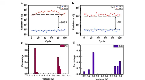
struc-tures is shown in Fig.3a and b. A device with Ag as an
upper electrode can have a resistance ratio of 103 and TaN as the upper electrode can reach 60. Both Ag and TaN top electrodes exhibit superior bipolar switching
[image:2.595.57.541.425.714.2]characteristics. The distribution of set and reset
op-eration voltage is presented as histograms in Fig. 3c
and d, respectively. The Ag/HfAlOx/Pt devices ex-hibit much lower SET voltage. The performances of the two structures are compared. The SET and RE-SET voltage rang of the Ag/HfAlOx/Pt devices was
from 0.33 to 0.62 V and from −1.3 to −1.5 V and
the TaN/ HfAlOx/Pt devices was from 0.8 to 1.8 V
and from −1.3 to −2 V. After comparison, it was
found that the device using Ag as the upper electrode
is more suitable as a device for implementing logic due to better stability and lower operating voltage.
Moreover, the switching mechanism of the two
types of structure is further expounded. The I–V
curves are analyzed in Fig. 4a–d. The curves are
taken in logarithmic coordinates to analyze the current status in the low-resistance state (LRS) and high-resistance state (HRS) states, respectively. It is
shown in Fig. 4a and b the current transportation of
Ag/HfAlOx/Pt devices exhibit ohmic current during
Fig. 2Typical current-voltage characteristics of Ag/HfAlOx/Pt (a) and TaN/HfAlOx/Pt devices (b)
[image:3.595.59.539.87.231.2] [image:3.595.60.538.438.701.2]the voltage sweeping. Whether applying a forward voltage or applying a negative voltage for
TaN/HfA-lOx/Pt devices shown in Fig. 4c and d, quasi-ohmic
current (slope is approximately equal to 1) is pre-sented in the LRS, while ohmic, quasi-ohmic, and
space charge limited current is presented in HRS at positive electric field.
The reason for this phenomenon is that the resistance change mechanism of TaN/HfAlOx/Pt devices is due to avalanching generation and recombination of the oxygen
Fig. 4The current fitting of the Ag/HfAlOx/Pt devices underapositive andbnegative electric fields and the current fitting of the TaN/HfAlOx/Pt devices undercpositive anddnegative electric fields
[image:4.595.56.540.88.359.2] [image:4.595.54.541.467.704.2]ion and oxygen vacancy dielectric layer. In Ag/HfAlOx/Pt devices, the forming and rupture of conducting filaments, thanks to the redox reactions of metallic Ag, can be driven by a much lower electric field.
In this experiment, low-resistance state (LRS) was de-fined as logic 1 and high-resistance state (HRS) as logic 0. The test diagram of IMP logic is shown in Fig.5a. It is im-plemented by two RRAM devices P and Q and one fixed load resistor. The states of P and Q are represented by p and q, respectively. IMP is performed by two simultaneous voltage pulses: Va and Vb (we defined Va > Vset > Vb and Va–Vb < Vset so that Va could program logic 0 to 1 and
Va−Vb could not program logic). The principle of logic p
change is due to q. If q equals 1, then p is left unchanged because the voltage drop across p is nearly Va−Vb, and if q equals 0, the p is always equals 1. The truth table for the
operation q←pIMPq is shown in Fig. 5b and the state
changes of P and Q with the pulse are shown in Fig.5c.
The NAND logic can be obtained through the two-step IMP logic. The implementation of NAND logic can be done by two-step IMP logic, because of the good uniform-ity. NAND is considered to be a universal logic, which means it can construct any Boolean logics through topo-logically connected NAND gates. As illustrated in Fig.5d, the operation was implemented in a circuit with three RRAM devices: P, Q, and S. The inputs were the values p and q which were stored in devices P and Q. In the first step of the execution logic, S is initialized to a 0 state. Then, two steps of IMP were executed:
s′←pIMPs (1).
s′′←qIMPs′(2).
The truth tables showing the equivalence of the sequence
of operations to NAND are shown in Fig.5e.
Conclusion
In summary, two kinds of devices (Ag/HfAlOx/Pt and TaN/HfAlOx/Pt) were fabricated in this study. Both devices show superior switching characteristics. Ag/HfA-lOx/Pt device has demonstrated advantages as a computing in-memory device such as CMOS compati-bility, good uniformity, low operating voltage, and low power consumption. Logic was implemented through Ag/HfAlOx/Pt RRAM devices. The realization of low operation voltage computing in-memory devices pro-vides an effective way to solve the traditional von Neu-mann structure difficulties in the future.
Abbreviations
ALD:Atomic layer deposition; HRS: High-resistance state; LRS: Low-resistance state
Acknowledgements
This work was supported by the NSFC (61704030 and 61522404), National Science and Technology Major Project (2017ZX02315005), the Program of Shanghai Subject Chief Scientist (18XD1402800), and the Support Plans for the Youth Top-Notch Talents of China.
Availability of Data and Materials All data are fully available without restriction.
Authors’Contributions
Z-YH prepared the HfAlO-based computing in-memory devices. Then Z-YH and T-YW designed the test methods and assembled the test equipment of in-memory computing. HZ, PZ, and S-JD revised the manuscript. LC, Q-QS, and D-WZ supervised the whole work. All authors critically read and ap-proved the final manuscript.
Competing Interests
The authors declare that they have no competing interests.
Publisher’s Note
Springer Nature remains neutral with regard to jurisdictional claims in published maps and institutional affiliations.
Received: 4 January 2019 Accepted: 27 January 2019
References
1. Backus, J. (2007). Can programming be liberated from the von Neumann style?: a functional style and its algebra of programs (p. 1977). ACM 2. Strukov DB, Snider GS, Stewart DR, Williams RS (2008) The missing
memristor found. nature 453(7191):80
3. Linn E, Rosezin R, Kügeler C, Waser R (2010) Complementary resistive switches for passive nanocrossbar memories. Nat Mater 9(5):403 4. Li H, Wang X, Ong ZL, Wong WF, Zhang Y, Wang P, Chen Y (2011)
Performance, power, and reliability tradeoffs of STT-RAM cell subject to architecture-level requirement. IEEE Trans Magn 47(10):2356–2359 5. Prodromakis, T. (2013). Two centuries of memristors. In Chaos, CNN,
memristors and beyond: a Festschrift for Leon Chua with DVD-ROM, composed by Eleonora Bilotta (pp. 508–517)
6. Yang Y, Mathew J, Pontarelli S, Ottavi M, Pradhan DK (2016) Complementary resistive switch-based arithmetic logic implementations using material implication. IEEE Trans Nanotechnol 15(1):94–108
7. Huang P, Kang J, Zhao Y, Chen S, Han R, Zhou Z et al (2016) Reconfigurable nonvolatile logic operations in resistance switching crossbar array for large-scale circuits. Adv Mater 28(44):9758–9764
8. Chua L (1971) Memristor-the missing circuit element. IEEE Transactions on circuit theory 18(5):507–519
9. Borghetti J, Snider GS, Kuekes PJ, Yang JJ, Stewart DR, Williams RS (2010) ‘Memristive’switches enable‘stateful’logic operations via material implication. Nature 464(7290):873
10. Chen Q, Wang X, Wan H, Yang R (2017) A logic circuit design for perfecting memristor-based material implication. IEEE Transactions on Computer-Aided Design of Integrated Circuits and Systems 36(2):279–284
11. Marranghello FS, Callegaro V, Martins MG, Reis AI, Ribas RP (2015) Factored forms for memristive material implication stateful logic. IEEE J Emerg Sel Topics Circuits Syst 5(2):267–278
12. Sun X, Li G, Ding L, Yang N, Zhang W (2011) Unipolar memristors enable “stateful”logic operations via material implication. Appl Phys Lett 99(7): 072101
13. Suh DI, Kil JP, Kim KW, Kim KS, Park W (2015) A single magnetic tunnel junction representing the basic logic functions—NAND, NOR, and IMP. IEEE Electron Device Letters 36(4):402–404
14. Kvatinsky S, Satat G, Wald N, Friedman EG, Kolodny A, Weiser UC (2014) Memristor-based material implication (IMPLY) logic: design principles and methodologies. IEEE Transactions on Very Large Scale Integration (VLSI) Systems 22(10):2054–2066
15. Niinistö L, Ritala M, Leskelä M (1996) Synthesis of oxide thin films and overlayers by atomic layer epitaxy for advanced applications. Materials Science & Engineering B 41(1):23–29
16. Becker, O. (1962). AN Whitehead and B. Russell, Principia Mathematica 17. Hennessy JL, Patterson DA (2011) Computer architecture: a quantitative