Single Active Element based Current-Mode All-Pass
Filter
Jitendra Mohan
Department of Electronics and Communication Engineering, Jaypee Institute of Information Technology,
Sector-128, Noida -201304(INDIA)
ABSTRACT
In this paper, a current-mode all-pass filter employing single multi-output dual-X second-generation current conveyor, a grounded resistor and a grounded capacitor is proposed. The circuit is as good as ideal for current-mode cascading by possessing low input and high output impedances. The use of grounded passive components makes the circuit, ideal for IC implementation. The effect of non-idealities and parasitics associated with the real MO-DXCCII implementation is also considered. The theoretical results are validated through PSPICE simulation program using 0.35µm CMOS process parameters.
Keywords
Active filters, current conveyor, all-pass filter, analog signal processing.
1.
INTRODUCTION
First order all-pass filter (APF), also called as a phase shifter is a simple and useful analog building block for many analog signal processing applications. The few important applications of interest are in delay equalization, in communication and instrumentation system, etc. [1-3]. Recently, the design of first order current-mode all-pass filter (CMAPF) is focused on the use of minimal number of components i.e. one active element and two passive components (minimum for first order active RC realization).
Numerous first order current-mode APFs employing different types of current-mode active elements such as second generation current conveyor (CCII) [5-6, 8-9, 11, 15-16, 18, 20, 27], four terminal floating nullor (FTFN) [7], third generation current conveyor (CCIII) [12, 17], Current operational amplifier (COA) [13], differential voltage current conveyor (DVCC) [14], current differencing buffered amplifier (CDBA) [10], dual-X second-generation current conveyor (DXCCII) [4, 19, 26] are available in the literature. Some of the current-mode all-pass filter circuits do enjoy the feature(s) of grounded components, minimum components, single active element, low-input and high-output impedances.
In this paper a novel first order current-mode all-pass filter is presented. The proposed circuit employs single active element and two grounded passive components. It also possesses low-input and high-output impedance feature with no element matching restriction. The proposed circuit is based on
multi-output dual-X second-generation current conveyor (MO-DXCCII) [21]. It is a useful and versatile current-mode active element for analog signal processing applications [22-24, 28-29]. The proposed circuit is validated through PSPICE simulation using TSMC 0.35µm CMOS process parameters.
2.
CIRCUIT DESCRIPTION
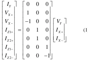
A MO-DXCCII is characterized by the following port relationship:
1
2
1
2
0
0
0
1
0
0
1 0
0
0
1
0
0
1
0
0
0
1
0
0
1
Y X
Y X
X Z
X Z
Z Z
I
V
V
V
I
I
I
I
I
I
(1)
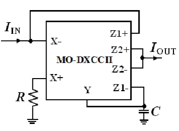
The symbol and CMOS implementation of MO-DXCCII are shown in Fig. 1. The proposed CMAPF using single MO-DXCCII and two grounded passive components is shown in Fig. 2. The circuit is characterized by the following transfer function
1 1 OUT
IN
I sCR
I sCR
(2)
The frequency dependent phase response (Φ) of the proposed circuit is given as
0 1
( ) 180 2tan ( CR)
(3)
[image:1.595.385.539.301.406.2](a)
(b)
[image:2.595.54.539.76.426.2]Fig 1: (a) Symbol, and (b) CMOS Implementation of MO-DXCCII.
Fig 2: Current-mode all-pass filter
It is worth mentioning that by interchanging the resistor and the capacitor in the Fig. 2 an additional all-pass filter circuit can be obtained. However the circuit would employ a grounded capacitor at the X terminal of MO-DXCCII, which does pose a high frequency limitation. It is a well known fact that the use of capacitor at the X terminal of the current conveyor circuit would pose a high frequency limitation [25].
3.
NON-IDEAL ANALYSIS
Considering the non-idealities of the MO-DXCCII into account, the port relationships of the terminal voltages and currents can be written as
1
2
1 1
2 2
1 3
2 4
0 0 0
0 0
0 0
0 0
0 0
0 0
0 0
Y
X
Y X
X Z
X Z
Z
Z I V
V V
I I
I I
I I
(4)
Here, α1 and α2 are the current transfer gains (deviate from
unity by the current tracking errors) from X+ terminal to Z1+ and Z2+ terminals respectively, α3 and α4 are the current
transfer gains from X- terminal to Z1- and Z2- terminals, respectively, and β1 and β2 are the voltage transfer gains
(deviate from unity by the voltage tracking errors) from Y input terminal to X+ and X- terminals, respectively. However, these transfer gains remain close to unity upto a very high frequency range (i.e. in GHz); the actual value depends upon the technology and the devices used in implementing the active element [25].
Taking the tracking errors of the non-ideal MO-DXCCII into account, the proposed circuit is reanalyzed and the modified transfer function is found to be as
4 2 1 3 4
1 3 1 OUT
IN
I sCR
I sCR
[image:2.595.80.258.476.606.2]From equations (5), it is to be noted that the non-idealities do affect the filter gain and the pole frequency. The active and passive sensitivities of the proposed circuit with respect to pole frequency (ωo) and gain (H) are as follows
1 3 1 2 4 2 1 2 1 2 3 4
, 1, , , 1, , , 0, , , , , , 0, , 1
o o o H H
C R C R
S S S S S
(6)
Equation (6) shows that the sensitivities are within or equal to unity in magnitude, thus ensuring good active and passive sensitivity performance.
4.
PARASITIC EFFECTS
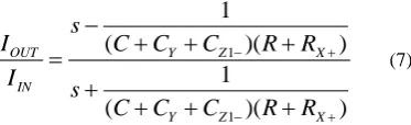
Next study is carried out on the effects of various parasitics of the MO-DXCCII employed in the proposed circuit. These are the Y and Z terminals parasitic capacitances and the X-terminal resistance. For the circuit of Fig. 2, the Y and Z1- terminal capacitances (CY and CZ1-) appear in shunt with external C and the X+ terminal resistance (RX+) appears in
series with external R, thus the modified transfer function is
1
1
1
(
)(
)
1
(
)(
)
OUT Y Z X
IN
Y Z X
s
I
C
C
C
R
R
I
s
C
C
C
R
R
(7)
From equation (7), it is to be further observed that most of the parasitic capacitances and resistances get merged with the external capacitor and resistor. Such a merger will cause a slight offset in circuit parameters, which can be corrected by pre-distorting the passive element values used in the circuit.
5.
SIMULATION RESULTS
The proposed circuit in Fig. 2 was simulated using the PSPICE simulation program with CMOS implementation of MO-DXCCII [21] using TSMC 0.35 µm process parameters as listed in Table 1. The supply voltages used were ± 1.8 V and VBB = -0.5 V and the aspect ratios of NMOS and PMOS
[image:3.595.311.548.87.282.2]transistors are listed in Table 2. The proposed circuit was designed for a theoretical pole frequency of 1.59 MHz. The designed values used were C = 100pF and R = 1 KΩ. The phase and gain plots are shown in Fig. 3, which shows a pole frequency of 1.57 MHz, which is close to the designed value. The phase is found to be vary from 1800 to 00.
Table 1. TSMC 0.35 µm CMOS process parameters.
NMOS:
LEVEL=3 TOX=7.9E-9 NSUB=1E17 GAMMA=0.5827871 PHI=0.7 VTO=0.5445549 DELTA=0 UO=436.256147 ETA=0 THETA=0.1749684 KP=2.055786E-4 VMAX=8.309444E4 KAPPA=0.2574081 RSH=0.0559398 NFS=1E12 TPG=1 XJ=3E-7 LD=3.162278E-11 WD=7.04672E-8 CGDO=2.82E-10 CGSO=2.82E-10 CGBO=1E-10 CJ=1E-3 PB=0.9758533 MJ=0.3448504 CJSW=3.777852E-10 MJSW=0.3508721
PMOS:
[image:3.595.92.279.301.358.2]LEVEL =3 TOX = 7.9E-9 NSUB=1E17 GAMMA=0.4083894 PHI=0.7 VTO=-0.7140674 DELTA=0 UO=212.2319801 ETA=9.999762E-4 THETA=0.2020774 KP=6.733755E-5 VMAX=1.181551E5 KAPPA=1.5 RSH=30.0712458 NFS=1E12 TPG=-1 XJ=2E-7 LD=5.000001E-13 WD=1.249872E-7 CGDO=3.09E-10 CGSO=3.09E-10 CGBO=1E-10 CJ=1.419508E-3 PB=0.8152753 MJ=0.5 CJSW=4.813504E-10 MJSW=0.5
Table 2. Transistor aspect ratios
Transistors W(µm) L(µm)
M1-M2 1.4 0.7
M3-M5 2.8 0.7
M17-M18 2.4 0.7
M19-M21 4.8 0.7
M6-M16, M22-M28 9.6 0.7
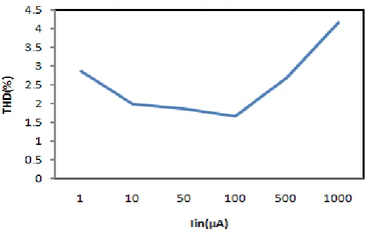
[image:3.595.130.459.561.714.2]Next, the circuit may use as a phase shifter introducing a 900 shift to a sinusoidal signal of pole frequency. The input and 900 phase shifted output waveforms are shown in Fig. 4, which verify the circuit as a phase shifter. In addition, the Fourier spectrums of the input and output currents, showing high selectivity for the applied input current are shown in Fig. 5. The total harmonic distortion (THD) variation with respect to the amplitude of the applied sinusoidal input current at 1.59 MHz is shown in Fig. 6. It can be seen that the THD value of the filter remains below 3% for the input current up to 1mA (peak to peak). Simulation results are quite agreed with the theoretical results.
Fig 3: Phase and gain plot for Circuit of Fig. 2
F r e q u e n c y
1 . 0 K H z 1 0 K H z 1 0 0 K H z 1 . 0 M H z 1 0 M H z 1 0 0 M H z 1 P ( I ( v o u t ) ) 2 D B ( I ( v o u t ) )
0 d 5 0 d 1 0 0 d 1 5 0 d 1
Fig 4: Input and 900 phase shifted output at 1.59MHz.
Fig 5: Fourier spectrum of the input and output signal at 1.59MHz
Fig 6: THD variation at output with signal amplitude at 1.59MHz
6.
CONCLUSION
This paper presented a first order current-mode all-pass filter suitable for cascading, employing minimum number of active and passive components (one MO-DXCCII, one grounded resistor and one grounded capacitor). The circuit enjoys low input and high output impedance feature, which is a desirable
feature for the current mode cascading. Beside this, the circuit employs grounded passive components, which are suited for IC implementation. The proposed circuit requires no matching constraints, possesses low active and passive sensitivities. The proposed circuit is validated by attractive simulation results.
T i m e
0 s 0 . 4 u s 0 . 8 u s 1 . 2 u s 1 . 6 u s 2 . 0 u s
I ( v o u t ) I ( i i n ) - 1 . 0 m A
0 A 1 . 0 m A
O U T P U T I N P U T
F r e q u e n c y
0 H z 4 M H z 8 M H z 1 2 M H z 1 6 M H z
I ( v o u t ) I ( i i n ) 0 A
[image:4.595.162.427.473.644.2]7.
REFERENCES
[1] S.J.G. Gift, “The application of all-pass filters in the design of multiphase sinusoidal systems”, Microelectronics Journal, 31, 9–13, 2000.
[2] D. Biolek, R. Senani, V. Biolková, Z. Kolka, “Active elements for analog signal processing: classification, review, and new proposals”, Radioengineering, 17, 2008.
[3] S.J.G. Gift, B. Maundy, “A novel circuit element and its application in signal amplification”, International Journal of Circuit Theory and Applications, 36, 219-231, 2008.
[4] J. Mohan, S. Maheshwari, “Cascadable current-mode first-order all-pass filter based on minimal components”, The Scientific World Journal, 2013, Article ID 859784, 5 pages, 2013.
[5] A.M. Soliman, “Realizations of an all-pass transfer functions using second generation current conveyor”, Proceedings of the IEEE, 68, 1035, 1980.
[6] M. Higashimura, Y. Fukui, “Realization of current mode all-pass networks using a current conveyor”, IEEE Trans. Circuits Syst., 37, 660–661, 1990.
[7] M. Higashimura, “Current-mode all-pass filter using FTFN with grounded capacitor”, Electronics Letters, 27, 1182–1183, 1991.
[8] A.M. Soliman, “Theorems relating to port interchange in current-mode CCII circuits”, International Journal of Electronics, 82, 582–604, 1997.
[9] A.M. Soliman, “New current mode filters using current conveyors”, International Journal of Electronics and Communications (AEÜ), 51, 275–278, 1997.
[10] A. Toker, S. Ozoguz, O. Cicekoglu, C. Acar, “Current-mode all-pass filters using current differencing buffered amplifier and a new high-Q band-pass filter configuration”, IEEE Transactions on Circuits and Systems II: Analog and Digital Signal Processing, 47, 949–954, 2000.
[11] I.A. Khan, S. Maheshwari, “A Simple first-order all-pass sections using a single CCII”, International Journal of Electronics, 87, 303-306, 2000.
[12] S. Maheshwari, I.A. Khan, “Novel first order all-pass sections using a single CCIII”, International Journal of Electronics, 88, 773–778, 2001.
[13] S. Kilinc¸ U.Cam, “Current-mode first-order all-pass filter employing single current operational amplifier”, Analog Integrated Circuits and Signal Processing, 41, 47– 53, 2004.
[14] S. Minaei, M.A. Ibrahim, “General configuration for realizing current-mode first order all-pass filter using DVCC”, International Journal of Electronics, 92, 347– 356, 2005.
[15] J.W. Horng, C.L. Hou, C.M. Chang, W.Y. Chung, H.L. Liu, C.T. Lin, “High output impedance current-mode first-order all pass networks with four grounded components and two CCIIs”, International Journal of Electronics, 93, 613-621, 2006.
[16] I.A. Khan, P. Beg, M.T. Ahmed, “First-order current mode filters and multiphase sinusoidal oscillators using CMOS MOCCIIs”, The Arabian Journal for Science and Engineering, 32, No. 2C, 119-126, 2007.
[17] S. Maheshwari, “Novel cascadable current-mode first-order all-pass section”, International Journal of Electronics, 94, 995–1003, 2007.
[18] S. Minaei, E. Yuce, “All grounded passive elements current-mode all-pass filter”, Journal of Circuits, Systems and Computers, 18, 31–43, 2009.
[19] S. Minaei, E. Yuce, “Unity/Variable-gain voltage-mode/current-mode first-order all-pass filters using single dual-x second-generation current conveyor”, IETE Journal of Research, 56, 305-312, 2010.
[20] J.W. Horng, C.L. Hou, Y.S. Guo, C.H. Hsu, D.Y. Yang, M.J. Ho, “Low input and high output impedances current-mode first-order all pass filter employing grounded passive components”, Circuits and Systems, 3, 176-179, 2012.
[21] A. Zeki, A. Toker, “The Dual-X Current Conveyor (DXCCII): A new active device for tunable continuous-time filters,” International Journal of Electronics, 89, 913-923, 2002.
[22] A. Zeki, A. Toker, “DXCCII-based tunable gyrator”, International Journal of Electronics and Communications (AEÜ), 34, 59-62, 2005.
[23] S. Minaei, “Electronically tunable current-mode universal biquad filter using dual-x current conveyors”, Journal of Circuits, Systems, and Computers, 18, 665– 680, 2009.
[24] S. Minaei, E. Yuce, “A new full-wave rectifier circuit employing single dual-X current conveyor”, International Journal of Electronics, 95, 777–784, 2008.
[25] A. Fabre, O. Saaid, H. Barthelemy, “On frequency limitations of the circuits based on second generation current conveyors”, Analog Integrated Circuits and Signal Processing, 7, 113-129, 1995.
[26] J. Mohan, B. Chaturvedi, S. Maheshwari, “Novel current-mode all-pass filter with minimum component count”, International Journal of Image, Graphics and Signal Processing (IJIGSP), 5, 32-37, 2013.
[27] J. Mohan, S. Maheshwari, “Two active elements based all-pass section suited for current-mode cascading” World Academy of Science, Engineering and Technology, International Journal of Electrical Engineering, 7, 1217 – 1221, 2013.
[28] S. Maheshwari, B. Chaturvedi, “High-input low-output impedance all-pass filters using one active element”, IET: Circuits Devices and Systems, 6, 103-110, 2012.