Design of Linear CMOS Transconductance Elements for
Alpha-Power Law Based Mosfets and an Automatic
Compensation Technique for Temperature
Bhaskar Gopalan
Independent Consultant, Chennai, India *Corresponding Author: [email protected]
Copyright © 2014 Horizon Research Publishing. All rights reserved.
Abstract
A model on alpha-power law MOSFETs based source-coupled differential pair (SCDP) is discussed and a simple design procedure for realizing a linear CMOS SCDP transconductance element is proposed. The proposed or modified SCDP circuit using this procedure is an alternative to that of conventional SCDP and the circuit discussed has superior linearity for a wide range ±(0-300mv) of input differential voltage at a supply voltage of 1.2v. The modified SCDP also includes the circuitry needed to suppress the variation in the quiescent current with respect to input common-mode voltage noise. The SPICE results are used to verify theoretical predictions. The results show close agreement between the predicted model behavior and the simulated performance. The simulated result on Total Harmonic Distortion (THD) shows that the modified SCDP circuit is better than the conventional SCDP by about four times at input differential voltage amplitude of ±100mv. An example circuit, a second order continuous time gm-C band-pass filter is constructed using the fully differential modified SCDP and the fully differential conventional SCDP circuit and the result shows that the modified transconductor circuit is better in linearity (THD) than the conventional SCDP by about two times at the input differential voltage amplitude of ±100mv. An automatic digital compensation scheme for temperature is also presented and the temperature coefficient of output current is reduced by about eight times to 250ppm/deg.C after compensation for the maximum change in temperature of 150deg.C and at the input differential voltage of 100mv.Keywords
CMOS Transconductor, SCDP Circuit, Linearity, Total Harmonic Distortion (THD), Gm-C Filter, SPICE Models, Temperature Compensation, Flash ADC1. Introduction
Linear transconductance elements [1]-[14] are useful in
building blocks in analog signal-processing systems and the literature on this topic is rich indeed. A cross-coupled quad cell is proposed by [1]. An inverter-based transconductor is discussed in [10] and [13]. In [9], a bias-offset cross-coupled transconductor is realized. In [1] and [8], the linearity with input differential voltage is achieved by CMOS pairs and floating voltage sources. In [6], the linearity is achieved with two additional PMOS SCDP pairs. The source degeneration linearization is used in [11]. A four MOS transistor cell to obtain a linear transconductor is realized in [12]. In [14], the linearity is obtained with a quadritail cell. In all of these transconductors discussed, only the square law devices are considered but in the present paper, a model for SCDP based on the alpha-power law devices is proposed.
The objective of this paper is to present a model for the alpha-power law based CMOS SCDP transconductors and a simple design procedure for the realization of linear CMOS modified SCDP transconductance block for both single-ended and fully differential outputs. The modified SCDP doesn’t require any special cell and includes the same circuit as required in a conventional SCDP as the base circuitry. Also the linearity and the input voltage range of the proposed design are superior to that of the conventional source-coupled differential pair. The computer simulation results are presented.
All MOSFET’s are assumed to be enhancement-mode types biased in saturation and the transistor behavior is approximated by the relation,
(
)
α(
)
gs ds
kp
I=
V -vth 1+λV
2
(1)where
vth
is the total threshold voltage inclusive of body-effect.kp=KP W/L
(
)
is the transconductance parameter, W and L are the width and length of the channel,λ
is due to the effect of channel length modulation andα
is the alpha-power law value.in the transconductance parameter is discussed in section-3. Section-4 proposes a simple design procedure used to cancel out the third degree term in the transconductance and to make a perfect linear transconductor. The section-4 also includes the circuitry that is needed to minimize the variation of quiescent current with respect to input common-mode voltage. The section-5 presents the results, one with alpha-power law devices and the other with square law devices for both SCDP and the modified SCDP. The section-6 describes on how the various output conductances (channel length modulation) are included in the present model for the fully differential modified transconductor. A gm-C band-pass filter based out of the conventional SCDP and the modified SCDP is described in section-7. Using this filter, a comparison between the conventional SCDP and the modified SCDP in terms of %THD is made in section-7. An automatic temperature compensation scheme for the discussed modified transconductor is also presented in section-8. Section-9 concludes about the modified SCDP circuitry based on alpha-power law MOSFETs.
2. Theory on Basic Cmos Scdp
Transconductor Based on
Alpha-Power Law Mosfets
Let
I
1 andI
2 be the drain currents in the two branches of the SCDP circuit (Fig.1) andV
gs1 andV
gs2 be thegate-source voltages of the respective NMOS MOSFETs in the SCDP.
vth
is the total effective threshold voltage of NMOS MOSFETs including body-effect. The body-effect’s dependence on input differential voltage is considered in section-3. Neglecting channel length modulation for time being (it is accounted later in the section-6), we have from (1) as,1/α 1/α
1 2
gs1
2I
gs22I
V =
+vth ; V =
+vth
kp
kp
(2)in gs1 gs2
V =V -V
; (3) Using (2) and (3), we obtain,( )
2/α
1/α
2 2/α 2/α
in
2
1 2 1 2V =
I +I -2 I I
kp
(4)Noting that
(
) (
2)
2 21 2 1 2 1 2 1 2
I -I
= I +I
-4I I =Iss -4I I
, (5) whereIss
is the quiescent current for SCDP.From (4) and (5), we have,
(
)
2/α 1/α
2
2 2/α 2/α 2
in
2
1 2 1/α2
1 2V =
I +I -
Iss - I -I
kp
4
(6)and this could be written using (2) as,
(
) (
2)
2 2 2(
)
2 1/αgs1 gs2 in 2/α 1 2
2
V -vth + V -vth -V = Iss - I -I kp
(7) Expanding (7) we arrive at,
2 2
D 1 2 α
kp
I =I -I = Iss -
VX
2
(8) whereVX
is given by(
)
α2 2 2 2
gs1 gs2 gs1 gs2 in
VX= V +V -2vth V +V +2vth -V (9) Let
V
cmbe the input common-mode voltage.V
P is thenode voltage at the point P in Fig.1. Let
V
gs1 andV
gs2be written as,
in
gs1 cm P
in
gs2 cm P
V
V =V +
-V ;
2
V
V =V -
-V
2
(10)
(
V +V
gs1 gs2)
=2 V -V
(
cm P)
(11) From equations (9), (10) and (11),VX
can be written as,( )
αV
in2 αVX= 2K
1-2K
(12) whereK
is given by(
)
2 in2cm P
V
K= V -V -vth +
4
(13)The differential current
I
D for a source-coupled pair can be written as,3
D 0 in 1 in
I =a V +a V +(higher order terms)
(14) and let biasing currentIss
be written as,2
0 q in
Iss=I +m V +(higherorder terms)
(15) Now consider in equations (8), (12) and (13), we have,( )
(
)
(
)
(
)
α 2 α 2 in 2α 2 cm P α 2 cm P V /4 kp 2K=kp V -V -vth 1+
2 2 V -V -vth
(16)
Expanding the curly bracket term by binomial series and neglecting higher order terms and noting that the above equation should be equal to
Iss
2 since the dc term of equation (14) is zero, we have equation (16) that could be written from equations (8), (12), (13) and (15) as,(
)
(
)
2 in
2 2 2 2 α 2
0 q 0 in 0 2
cm P
αV /8 Iss I +2m I V kp K I 1+
V -V -vth
≈ ≈ ≈
(17)
(
)
(
0)
q 2/α
0
αI /16
m =
I /kp
(18)where
α
0 cm P
I =kp(V -V -vth)
. (19) Now writing equation (12) by binomial series, we obtain,( )
4 2in α in
2 α α-1 V
αV higherorder
VX=(2K) 1- +
-2K 8K terms
(20)
provided
in
V
≤
2K
(21) where(
)
2α
K = Iss/kp
(22) Substituting equations (20) and (22) in equation (8) we arriveD
I
after neglecting higher order terms as,( )
2D m in in
α-1
I =G V 1-
V
4K
(23)where
m
α
G =
Iss
2K
(24)Equations (23) and (24) constitute the required equations for the output differential current which are similar to the one in square law based SCDP circuit.
3. Condition for the Compensated SCDP
LetIss
be written as,(
)
2
0 in
Iss=I +mV + higher order terms
(25) with new ‘m
’ in equation (15) required to cancel out the cubic degree dependency ofI
D onV
in.Considering only the second degree dependency on
V
in, we haveIss
can be written as ,2
0 in
Iss=I +mV
(26) Equation (26) accounts for all second degree input differential voltage effects including theV
P andvth
dependence on 2 in
V
.Substituting (25) in (23), we get
(
)
{
( )
(
)
2-2/α
1/α 2
D in 0 in
1/2
2/α 2 2-4/α
in 2
0 in
α
I =
kp V
I +mV
2
α-1 kp V
-
I +mV
4
(27)
Which upon expanding by binomial series and grouping like
terms can be written as (also by neglecting higher order terms),
{
(
)
( )
1/α 2-2/α 2 2-2/α
D in 0 in 0
0 1/2 2/α 2-4/α 0
m 2-2/α
α
I
kp V I
+V I
2
I
α-1 kp
-I
4
≈
(28) provided 0 inI
V
m
≤
(29)The equation (28) shows that the term in the square bracket should be zero to achieve a linear transconductance. This result can be stated as,
(
)
(
0)
2/α 0αI /8
m=
I /kp
(30)For square law based SCDP circuit,
m=kp/4
(31) Equation (31) is the result obtained by [1] for a square law based SCDP circuit. Equation (30) is the required condition to eliminate third degree term in the transconductance value in equation (23). Also to be noted is the following relation between the condition ‘m’ required to cancel out the cubic degree dependency ofI
D onV
in and the coefficient ‘mq’in Iss for a basic SCDP.
q
m=2m
(32) Equation (32) implies that twice the variation ofIss
with respect to 2in
V
than conventional SCDP is required forI
Dto cancel out the cubic degree dependency. Consider in Fig.1, V can be written as, P
2
P P0 in
V =V +δV
(33) The threshold voltagevth
is given approximately by,(
)
1 s P s 2 P
vth=vth0+K
Φ +V - Φ +K V
(34) whereK
1andK
2are due to non-uniform substrate doping andΦ
sis the surface potential.Using equation (33),
vth
can be written as,2
2 in
1 s 2 P0 2 in
s δV 1
vth=vth0+K Φ S 1+ - +K V +K δV Φ S S
(35)
where
S
is given by,P0
s
V
S=1+
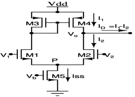
Figure 1. The Conventional Source-coupled pair – (Single ended output). V1=Vcm+Vin/2 and V2=Vcm-Vin/2 ; Vin=V1-V2.
Figure 2. The Modified Source-coupled pair – (Single ended output). V1=Vcm+Vin/2 and V2=Vcm-Vin/2; Vin=V1-V2.
Figure 3. The current source block as in Fig.2.
Expanding the bracket term in the above equation (35) by binomial series, we obtain after neglecting higher order terms as,
( )
21 s 2 P0 P in
vth vth0+K Φ
≈
S-1 +K V +δK V
(37)provided
s
in
Φ S
V
δ
≤
(38) whereK
Pis given by,1
P 2
s
K
K =K +
2 Φ S
(39)From equations (19), (33) and (37), we have the modified
I
0as,
(
)
α(
P)
in2 α' 2 α
0 cm P0 in PM
PM δ 1+K V I =kp V -vth-V -δV =kpV
1-V
(40)
where
( )
(
)
PM cm 1 s P0 2
V = V -vth0-K
S-1 Φ -V 1+K
(41) Writing the equation (40) by binomial series, we obtain (after neglecting higher order terms and keeping only the 2in
V
term) as,(
)
2P in
' α 2
0 PM 0M qm in
PM
αδ 1+K V
I
kpV
1-
=I -m V
V
≈
(42)provided
(
PM)
in
P
V
V
δ 1+K
≤
(43)where
α
0M PM
I =kpV
(44) and(
P)
0M qmPM
αδ 1+K I
m =
V
(45)Now the biasing current from equation (26) can be rewritten as,
(
)
20M in
[image:4.595.66.295.491.662.2]Iss=I +m new V
(46) [image:4.595.315.552.534.728.2]Equation (26) includes all the effects varying with second degree input differential voltage (including the effects of
P
V
andvth
varying with 2 inV
) and the equation (46) is rewritten from (26) only to include higher order terms other than 2in
V
term. Them new
(
)
value accounts for these higher order terms in addition. The zero differential voltage based currentI
0M is the same asI
0. Now the modified‘
m
’ can be rewritten from equation (30) using equation (42) as,(
)
2/α( )
' 1-2/α 2/α 2 1-2/α0 0M qm in
α
α
m new = kp
I
= kp
I -m V
8
8
(47) Upon expansion of
m new
(
)
value by binomial series and neglecting higher order terms, we get the following equation.(
)
0M 2/α(
)
qm 2in
0M 0M
1-2/α m
αI
kp
m new
1-
V
8
I
I
≈
(48)Now
Iss
can be written from using equations (46) and (48) as,(
)
(
)
(
)
4 2 qm in 0M in0M 2/α 2/α
0M 0M
α 1-2/α m V
αI V
Iss=I +
-8 I /kp
8 I /kp
(49)The inclusion of
V
P andvth
varying with 2 inV
has already been accounted in the second term of above equation (49) and its effect makes explicit presence in the third term of equation (49). The modified ‘m
’ after neglecting higher order terms can be written as,2/α 0M 0M
αI
kp
m(new)=
8
I
(50) which is same as the equation (30).The next section discusses on how to achieve the condition (50) to make a perfect linear transconductor.
4. Design of Modified SCDP with
Compensation for Linearity
The modified SCDP circuit with compensation for linearity is shown in Fig.2 and Fig.3. This is exactly the same circuit as the basic SCDP but with a little difference in the biasing circuit.
The ‘
m
’ value can be obtained from the low value of biasing resistorR
(Fig.2) as described below. The input CM voltage,V
cm is sensed from input voltages throughR
cmasshown in Fig.2 and this
V
cmbecomes the output CM voltageof the first stage for the next stage of modified SCDP circuit if any. The value of
R
cmshould be high to avoid anyloading on the output. From Fig.2 and Fig.3, we obtain
Iss
using equation (33) as,
(
)
s1 x cm
P P
1 out
V - V -V
V V
Iss=
-R R R
+ (51)
= P0
(
s1 x cm)
in2out 1 out
V -V +V
1 1 1 1
V + - + + δV
R R R R R
(52)
where
R
is the biasing resistor andR
1 is the resistor asshown in Fig.3.
R
out is the output resistance seen from thepoint
P
as shown in Fig.3.V
s1 andV
x are the fixedpotentials as shown in Fig.3.
R
2andV
x provide the valueof (
V -V
x cm) for equation (51) as per Fig.3. HereR
2ischosen to be much larger than
R
andR
1for reduced powerconsumption.
From (46) and (52), we find,
(
)
out
1 1
m new = + δ
R R
(53) and
0M P0 P
out
1 1
I =V + -I
R R
(54) where
s1 x cm P
1
V -V +V I =
R
(55)
Note that due to noise voltage changes in
V
cm , the quiescent currentI
0M varies and changes the outputcommon-mode voltage. Without
I
P current, the low value ofR
leads to larger variation inI
0Mwith respect toV
cm.The circuits shown in Fig.2 and Fig.3 provide the value of
0M
I
with lesser variation with respect toV
cm at dc. Bydifferentiating
I
0Mwith respect toV
cmin equations (54)and (55), we get,
(
)
0M P0
out bs
cm out cm 1
I = 1+ 1 +s C +2C V - 1
V R R V R
∂ ∂
∂ ∂ (56)
where
C
outis the output capacitance of the current source blockI
P seen from the point P as in Fig.3 andC
bs is thebulk-to-source capacitance of the transistor M1or M2. By differentiating equation (19), we obtain as,
1/α
P0 0M 0M
cm 0M cm
V =1-1 I 1 I
V α kp I V
∂ ∂
∂ ∂ (57)
By substituting (57) in (56), we obtain as,
(
)
(
)
out bs out 1 0M 1/α cm 0M out bs out 0M1+ 1 +s C +2C - 1
R R R
I =
V 1 1 1 I 1
1+ + +s C +2C
R R α kp I
and
1/α
0M m
cm 0M cm
I
G
=
α kp
1-
1
V
2 I
α V
∂
∂
∂
∂
(59)By making
R
1
R
, we haveI
0Mthat varies minimallywith respect to
V
cmat dc as shown in equation (58). A fully differential circuit can be made with two single ended SCDP circuits as shown in Fig.4. The following design procedure steps are required to design a compensated fully differential modified SCDP transconductor.1. The value of quiescent current (
I
0M) andkp
shouldbe chosen to achieve the transconductance (
2G
m) fora fully differential circuit (Fig.4) as required for the given design specifications.
2. The biasing resistor (
R
) should be adjusted to provide the required value of ‘m
’ as in equation (53) for compensation.3. The value of sourcing current (
I
P) in equation (55) needs to be tuned to provide the required value ofI
0Mas in equation (54). That is, the potentials
V
s1 and xV
are to be chosen accordingly. Note that in the modified SCDP, the power dissipation is more than the conventional SCDP due to this sourcing current and the opamp’s power supply currents as in Fig.3.The current
I
0M also varies with the input differentialvoltage amplitude as per equation (46). If we assume a single sinusoidal input differential voltage of amplitude
V
a andfrequency
ω
in Fig.2, the value ofIss
is,(
)
( )
(
)
(
)
(
)
2 2
0M a
2 2
a a
0M
Iss=I +m new V sin ωt
m new V m new V
=I +
-
cos 2ωt
2
2
(60)
Note here that the dc value of
Iss
is changed and is more due to the input differential voltage amplitude. At higher input differential amplitudes, the dc currentI
0M is more and this is the reason why two transconductors based fully differential circuit is studied and not a single transconductor based fully differential circuit. In a single transconductor based fully differential circuit, asI
0M increases there is noroom to accommodate the increased current,
I
0M in M3 and M4 as the gate voltage of these two transistors is fixed (M3 and M4 operate as current sources). Hence, the output common-mode voltage drops due to the channel length modulation effect. In a two transconductors based fully differential circuit (Fig.4), asI
0M increases, thetransconductances (
g
m) of M3 and M4 (M3 and M4 arecurrent mirrors) increase and hence the output common-mode voltage tries to maintain approximately at the same level.
5. Results on Transconductors
The SPICE model library chosen for simulation is 130nm,1.2v, IBM Technology process. There are two examples for a fully differential transconductor shown here, one with alpha-power law characteristic and the other with square law characteristics.
Example 1: At higher biasing currents of SCDP, the MOSFETs behave deviated from square law characteristic for the chosen model library. The biasing current is chosen as
0M
I
=310uA. From model library,KP
=40uA/vα,vth0
=0.366v,
α
=1.17 andVdd
=1.2v. The differential pair MOSFETs haveW
=20u andL
=0.15u .The ideal value of transconductance2G
m(fully differential) is 5.4mA/v. Thevarious design parameters are
V
cm=0.65v,V
x=1.15v,V
P0=71mv,
R=R
1=0.12k,V
s1=0.5328v andδ
=0.59/v. Fromequation (50),
m new
(
)
=5.87mA/v2 but the realized valueis 4.9mA/v2.
The SPICE simulated differential output current versus input differential voltage characteristics (for input
V
cm=0.65v and output
V
cm=0.65) are shown in Fig.5 for ideal (straight line), conventional SCDP and modified SCDP circuits.The normalized linearity error in % vs input differential voltage characteristics are given in Fig.6 for both SCDP and modified SCDP circuits.The transient simulations were performed with a sinusoidal input frequency of 100MHz and an output load capacitance of
C
L=10pf. The obtained % total harmonicdistortion (%THD) Vs input differential voltage amplitude characteristics are shown in Fig.7. It is noted that at higher input voltages the distortion is higher for conventional SCDP than modified SCDP.
A change of 4.42% in quiescent current
I
0Mis observed for 20mv input common-mode voltage noise atV
in=50mvfor the fully differential modified SCDP whereas for the fully differential conventional SCDP, the change in
I
0M is8.03%.
Also a change in output common-mode voltage of 6.92% is noticed as the input differential voltage amplitude is changed from
V
in=10mv to 300mv at inputV
cm=0.65v for the fully differential modified SCDP whereas for the fully differential single transconductor based conventional SCDP, the change is 62.62% (A high change in output CM voltage!!!).The output noise spectral voltage density at 100MHz for this example-1 transconductor design is 64.7nv/√Hz (for both conventional and modified SCDP) without any output load capacitor. The input referred noise spectral voltage density at 100MHz is 3.4nv/√Hz.
vth0
=0.366v,α
=2.0 andVdd
=1.2v. The differential pair MOSFETs haveW
=20u andL
=0.15u. The ideal value of2G
m(fully differential) is 970uA/v. The designparameters are
V
cm=0.65v,V
x=1.2v,R=R
1=0.5k,V
P0=144mv,
V
s1=0.6715v andδ
=0.8/v. The realized value of(
)
m new
is 1.56mA/v2 but its theoretical value is1.33mA/v2.
The simulated output differential current versus
V
incharacteristics (for input
V
cm =0.65v and outputV
cm=0.65v) are shown in Fig.8 for ideal, conventional SCDP and modified SCDP circuits. Fig.9 shows the normalized errors in % Vs
V
incharacteristics for both SCDP and modifiedSCDP.
The obtained % THD Vs
V
in(amplitude) characteristicsare shown in Fig.10 for an input frequency of 100MHz and with an output load capacitance of
C
L=10pf.For this case, a change of 5.8% in quiescent current
I
0Mis obtained for 20mv input common-mode voltage noise atin
V
=50mv for the fully differential modified SCDP whereas for the fully differential conventional SCDP, the change in0M
I
is 2.39% .Also a change in output common-mode voltage of 6.29% is noticed as the input differential voltage amplitude is changed from
V
in=10mv to 300mv at inputV
cm=0.65v for the fully differential modified SCDP whereas for the fully differential single transconductor based conventional SCDP, the change is 36.46% (A high change in output CM voltage!!!).For this example-2, the output noise spectral voltage density at 100MHz is 115nv/√Hz for both conventional and modified SCDP circuits without any output capacitor. The input referred noise spectral voltage density at 100MHz is 6.7nv/√Hz.
6. The Effect of Output Conductances
Consider a fully differential modified SCDP as shown in Fig.4.Let
I
D1 andI
D2 be the output currents of the eachsingle transconductor and let
g
ds1 andg
ds2 be the outputconductances of transistors M1 and M3 (or M2 and M4) respectively. Let
V
o1 andV
o2 be the output voltages ofeach transconductor in a fully differential circuit. Let ' o1
V
and ' o2
V
be the output voltages at the opposite sides (M1 and M3) of each transconductor. Now we have the output currents as,(
)
' ' '
m in
D1 ds1 o1 L gs o1 ds2 o1
m in
ds1 o1
G V
I = +g V +s C +2C V N-g V
2 -G V
- +g V
2 (61)
(
)
' ' ' m inD2 ds1 o2 L gs o2 ds2 o2
m in
ds1 o2
-G V
I = +g V +s C +2C V N-g V
2 G V
- +g V
2 (62)
where
g
m is the transconductance of transistor M3 or M4and
C
gsis the gate-to-source capacitance of M3 or M4.where
m
m ds2
g
N=
g +g
(63)and
'
L L o
C =C +C
(64) whereC
L is the load capacitance atV
o1 andV
o2 ando
C
is the sum of bulk-to-drain capacitances of M2 and M4 (or M1 and M3) respectively as shown in Fig.2. The voltages' o1
V
and ' o2V
can be obtained from,(
) (
)
(
)
' m in
L o2 ds1 ds2 o1
'
o1 '
ds1 L gs
G V
sC V +
1+N - g +g
V
2
V =
g +s C +2C
N
(65)
(
) (
)
(
)
' m in
L o1 ds1 ds2 o2
'
o2 '
ds1 L gs
G V
sC V -
1+N - g +g
V
2
V =
g +s C +2C
N
(66)
The output voltage is given by,
(
D1 D2)
o o1 o2 '
L
I -I
V =V -V =
sC
(67)Substituting equations (65), (66) and (67) in equations (61) and (62), we obtain
V
oas,(
)
m ' L o ds1 ds2 ' LG 1+N
sC
V =
g +g
1+
sC
(68)Where
N
and ' LC
are defined in (63) and (64) respectively. The equation (68) shows the effect of various output conductances onV
o. Using example-1 as discussed in theprevious section, we have 4.48% change in
V
o due tooutput conductances neglecting
C
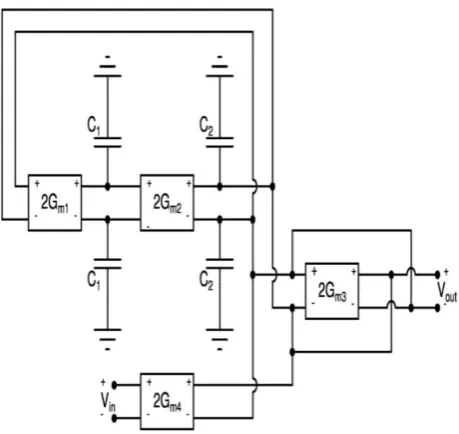
o. For the example-2 in the previous section, the change is 2.56% due to output conductances.A second-order continuous time Gm-C bandpass filter is constructed using both fully differential conventional SCDP and modified SCDP circuits. This circuit is shown in Fig.11.
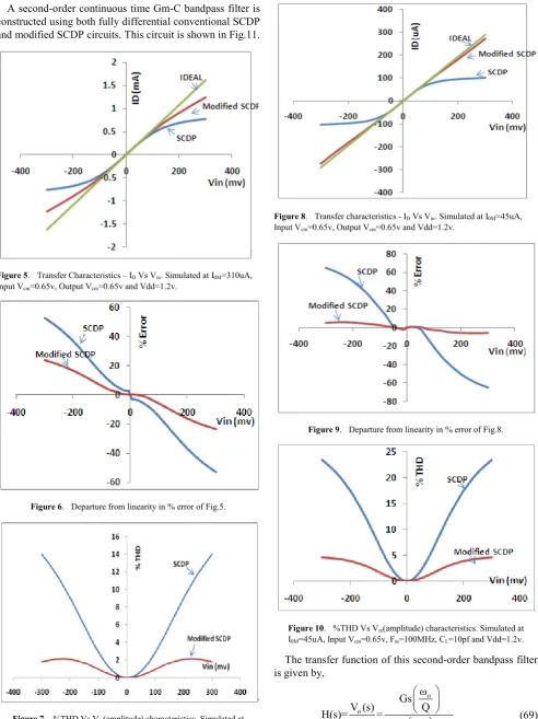
Figure 5. Transfer Characteristics – ID Vs Vin. Simulated at I0M=310uA,
Input Vcm=0.65v, Output Vcm=0.65v and Vdd=1.2v.
[image:8.595.60.553.75.733.2]Figure 6. Departure from linearity in % error of Fig.5.
Figure 7. %THD Vs Vin(amplitude) characteristics. Simulated at
I0M=310uA, Input Vcm=0.65v, Fin=100MHz, CL=10pf and Vdd=1.2v.
Figure 8. Transfer characteristics - ID Vs Vin. Simulated at I0M=45uA,
Input Vcm=0.65v, Output Vcm=0.65v and Vdd=1.2v.
Figure 9. Departure from linearity in % error of Fig.8.
Figure 10. %THD Vs Vin(amplitude) characteristics. Simulated at
I0M=45uA, Input Vcm=0.65v, Fin=100MHz, CL=10pf and Vdd=1.2v.
The transfer function of this second-order bandpass filter is given by,
o o
2 2
i o
o ω Gs
V (s) Q
H(s)= =
V (s) s +s ω +ω Q
Where G is the gain and is chosen as 1.0 at the center frequency.
o m3
m1 m2 m4
o
1 2 2 2
ω
2G
2G
2G
2G
ω =
=
and
=
=
C
C
Q
GC
C
(70)The various design parameters chosen are
o
ω =2π*100.0e06 rad/sec
,Q=4
,C =C =6.175pf
1 2 ,m1 m2
2G =2G =3.88mA/v
andm3 m4
2G =2G =0.97mA/v
.The bulk-node of all the NMOS transistors is tied to ground whereas bulk-node of all the PMOS transistors is tied to
Vdd
. The input common-mode voltage is chosen ascm
V
=0.65v. The biasing voltage (V
b) in the biasing circuit (Fig.1) is adjusted to provide all the required transconductance values for the case of conventional SCDP. For modified SCDP, the resistor (R
) and the current (I
P) in [image:9.595.312.553.198.312.2]the biasing circuit (Fig.2) are adjusted to provide all the wanted transconductances. Any suitable gain (
G
) can be achieved by independently varyingG
m4.Figure 11. A second order Gm-C Bandpass Filter using fully differential transconductors
The 3dB bandwidth obtained is around 40MHz both for the conventional and the modified SCDP. The transient simulations were carried out for an input frequency of 100MHz with different input differential voltages. The obtained values of total harmonic distortion in % for different input voltage amplitudes are tabulated in Table.1 for both conventional and modified SCDP. Also the power dissipated by the bandpass filter circuit is tabulated in Table.1 for various
V
in and both for the conventional SCDP and the modified SCDP.This filter can be operated at any center frequency and the higher frequency limitation is imposed by the sum of
bulk-to-drain capacitances (
C
o) of NMOS (M2 or M1) andPMOS (M4 or M3) in the individual transconductors as shown in equations (64) and (68). As long as the sum of load capacitance and the total bulk-to-drain capacitances (
C
o) ofM2 and M4 is equal to
C
1orC
2, the circuit can operate athigher center frequencies. In the present BPF circuit, the circuit operates up to 960MHz as the center frequency.
Table 1. The Band-pass Filter Performance Parameters studied in section-7.
Performance
Parameters (amplitude) Vin=50mv V(amplitude) in=100mv (amplitude) Vin=250mv Conventional
SCDP %THD Power Dissipation
0.166 %
1.90mW 1.93mW 0.540 % 1.97mW 2.295 %
Modified SCDP %THD
Power Dissipation
0.094 %
2.68mW 2.77mW 0.314 % 3.11mW 0.802%
8. A Temperature Compensation
Scheme for the Modified
Transconductor
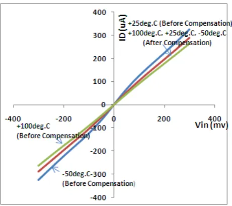
[image:9.595.63.293.355.572.2]The various output current versus input differential voltage characteristics for different values of temperature (-50deg.C, 25deg.C and 100deg.C) before compensation and after compensation (as explained below) for the case of example-2 studied in section-5, are shown in Fig.14. A temperature compensation circuit for the modified SCDP is shown in Fig.12. A two 2-bits digital technique has been used to compensate for the temperature above 25deg.C and below 25deg. C just to illustrate for the example-2, discussed in section-5.
Figure 12. A Temperature compensated biasing circuitry.
It is observed that above 25deg.C without temperature compensation, the
G
mvalue is lower and hence it requires [image:9.595.320.549.515.688.2]25deg.C, the modified transconductor requires less quiescent current. The Fig.12 is used to provide this adjusted biasing current value based on temperature. The designed values of
N
R
andR
P are 11.06k and 58.13k.The current
I
R, and hence the dropV
R in Fig.13 is usedto sense the temperature(T) variation. For the example-2 discussed in section-5, the drop
V
R varies from 0.440v(-50deg.C) to 0.487v (deg.100C). The designed value of
R
[image:10.595.67.291.209.335.2]R
is 2.15k.Figure 13. A temperature sensing circuitry for the modified SCDP.
[image:10.595.314.549.239.598.2]A flash Analog-to-digtal converter (ADC) as shown in Fig.15 is used to get the bits
B
2,B
1(for T>25deg.C) and thebits
B
2P,B
1P(for T<25deg.C) from the dropV
Rwhichvaries with respect to temperature. These bits are obtained directly from the
V
Rdrop using this ADC and hence themodified transconductor is automatically compensated for temperature. The high dc gain comparators are used in Fig.15. The upper half of Fig.15 is for temperatures > 25deg.C and the lower half is for temperatures < 25deg.C. The designed values of various parameters used in Fig.15 are
F
I
=1u,R
F =2.8k,R
G =10k,V
N1=0.474v andV
N2=0.447v.
Figure 14. ID Vs Vin Characteristics for different temperature corners.
Simulated at I0M=50uA, Input Vcm=Output Vcm=0.65v and Vdd=1.2v
For the case of example-2 studied in section-5, the temperature coefficient of output current before
compensation is 2081ppm/deg.C at
ΔT
=150deg.C(maximum),
V
in=100mv, inputV
cm=0.65v and0M
I
=50uA and the new value of temperature coefficient after compensation is 256ppm/deg.C.For the example-1 studied in section-5, the temperature coefficient of output current before compensation is 2914ppm/deg.C at
ΔT
=150deg.C(maximum),V
in=100mv, inputV
cm=0.65v andI
0M=310uA whereas the new value of temperature coefficient after compensation is 563ppm/deg.C.Figure 15. A Flash ADC for Temperature Compensation.
9. Conclusions
[image:10.595.63.294.521.726.2]common-mode voltage noise was minimized in the proposed design. The output differential voltage dependence on the transistor output conductances has been discussed. An example circuit, a Gm-C bandpass filter has been used to verify linearity in the transconductance value between the fully differential modified SCDP and the fully differential conventional SCDP. An automatic temperature compensation technique for the transconductance value has also been discussed.
REFERENCES
[1] Nedungadi and T.R.Viswanathan, “Design of Linear CMOS Transconductance Elements”, IEEE Trans. On Circuits and Systems, Vol. CAS-31, No.10, Oct.1984.
[2] David Johns and Ken Martin, “Analog Integrated Circuit Design”, John Wiley & Sons, Inc., 1997.
[3] Behzad Razavi, “Design of Analog CMOS Integrated Circuits”, McGraw Hill, Inc., 2001.
[4] R.Jacob Baker, Harry W.Li, and David E.Boyce, “CMOS – Circuit Design,Layout, and Simulation”, IEEE Press, 1998. [5] T.Sakurai and A.R.Newton, “A simple MOSFET model for
circuit analysis”, IEEE Trans. on Electron Devices, vol.38, no.4, Apr.1991.
[6] Bhaskar Gopalan, “A Linear CMOS Transconductance Element”, International Journal of Design, Analysis and Tools for Integrated Circuits and Systems,Vol.3, No.2,
Nov.2012.
[7] K.Bult and H.Wallinga, “A class of Analog CMOS Circuits based on the square-law characteristics of a MOS transistor in saturation”, IEEE J. of Solid-State Circuits, vol.22, pp.357-365, June 1987.
[8] E.Seevinck and R.F.Wassenaar, “A versatile CMOS Linear Transconductor/Square-Law function Circuit”, IEEE J. of Solid-State Circuits, vol.22, pp.366-377, June 1987.
[9] Z.Wang and W. Guggenbuhl, “A Voltage-Controlled Linear MOS Transconductor Using Bias Offset Technique”, IEEE J. of Solid-State Circuits, vol.25, pp.315-317, Feb. 1990. [10] C.S.Park and R.Schaumann, “A High-frequency CMOS
Linear Transconductance Element”, IEEE Trans. On Circuits and Systems, Vol.33, pp.1132-1138, Nov.1986.
[11] T-K.Nguyen and Sang-Gug Lee, “ Low-voltage, Low power CMOS operation Transconductance Amplifier with Rail-to-Rail Differential input range”, IEEE Symposium on Circuits and Systems, 2006.
[12] Mohamed O.Shaker, Soliman A.Mahmoud and Ahmed M.Soliman., “New CMOS Fully Differential Transconductance and Amplification for a Fully-Differential Gm-C Filter”, Electronics and Telecommunication Research Institute Journal (ETRI), vol.28, No.2, April 2006.
[13] Nauta, “A CMOS transconductance-C filter technique for very high frequencies”, IEEE J. Solid-State Circuits, vol.27, no.2, Feb.1992.