Designing a Full Adder Circuit Based on
Quasi-Floating Gate
Sahar Bonakdarpour, Farhad Razaghian
Department of Electrical Engineering, Azad University, South Tehran Branch, Tehran, Iran Email: [email protected], [email protected]
Received 2013
ABSTRACT
Since in designing the full adder circuits, full adders have been generally taken into account, so as in this paper it has been attempted to represent a full adder cell with a significant efficiency of power, speed and leakage current levels. For this objective, a comparison between five full adder circuits has been provided. Applying floating gate technology and refresh circuits in the full adder cell lead to the reduction of leakage current on the gate node. The simulations were ac-complished in this paper, through HSPICE software and 65 nm CMOS technology. The simulation results indicate the considerable efficiency of power consumption, speed and leakage current in the full adder cell rather than other cells.
Keywords: Floating Gate Transistor; Full Adder Circuit; Leakage Current; Quasi Floating Gate Transistor; Refresh Circuit
1. Introduction
Due to the point that the addition of binary numbers is the fundamental and most often used operation, and also the full adder circuit is very important in any design, so that within the high efficiency of full adder circuit, the efficiency of system increases as well. Today, Advance-ment of Technology has led to emergence of more wire-less and portable devices. For this, Low Power Circuits are needed more. To reduce the power dissipation in a CMOS circuit, the characteristics of power and the ef-fects of circuit have to be specified.
The most important factor in the design technology of low power and the approximation of power is dynamic power dissipation. As said, transistor size optimization is one method to reduce the power dissipation of Circuits in which the reduction of the transistor size leads to the reduction of power, by which finally the leakage current would be increased [1]. Also, we describe a new method for glitch power reduction based on threshold voltage adjustment, by which based on the following equation within the threshold voltage reduction, the leakage cur-rent will continue to increase exponentially with each generation, we could refer to (2) to verify this matter[2].
0 0
gs th
v v nvt leakage
I W W I e (2) where Vt, Vgs and Vth are respectively the thermal voltage,
gate-source voltage and threshold voltage. Therefore, today beside power reduction, the reduction of leakage current has concerned the electronic circuits’ designers.
In present paper, it has been attempted to introduce the full adder circuit with high efficiency within the low power dissipation, high speed and low leakage current.
2. Floating Gate and Quasi Floating Gate
MOS Transistors (FGMOS Transistors)
To reduce the dissipation power, the source voltage closed to the threshold voltage in NMOS and PMOS transistors has to be decreased. Through this, we could apply several inputs in a transistor gate, while in CMOS method only one input for each transistor is needed. The other reason to use FGMOS transistors is that in sub- threshold region, CMOS transistors are not involved high speed, so that, FGMOS transistors would be a better choice[3].
As shown in Figure 1, FGMOS transistor is a multiple input MOS transistor with isolated gate. Through a ca-pacitor, inputs are connected to transistor gate .These capacitors are called floating gate capacitors [4]. DC voltage on the floating gate is relevant with the capacitor ratio from the floating gate. FGMOS transistor could be considered as MOS transistor with a varied threshold voltage [5]. Due to the change in floating gate capacitor’s capacitances, the change in threshold voltage occurs .For this, FGMOS transistors in comparison with CMOS sistors would be a better choice. NMOS and PMOS tran-sistors with floating gate have been shown in Figure 1.
floating gate decrease [6]. The combination of the refresh circuit with floating gate transistor is called Quasi float-ing gate circuit (QFGMOS). In most FGMOS designs with high leakage on the floating gate, the method “Quasi floating gate” is recommended to be used. In present paper, the full adder circuit has been designed with “Quasi floating gate” method.
In the method “Ramirez-Angulo” and “Yin”, we use the resistor on the gate which this leads to the increase of dissipation power [7,8]. In most papers, instead of resis-tor, we use transistor. It could be said that the resistors could be replaced with the transistors “M3 and M4” in the Figures 2, 3 and 4 [9- 11]. The extra circuits on the gate are called the refresh circuits. Adding the refresh circuits on the gate node of floating gate transistor put the most effect on power, delay and occupied space, but the rapid advancement of technology and the reduction of gate oxide thickness bring about the problems in the gate leakage by which using the circuits would be un-avoidable.
[image:2.595.361.484.202.335.2]In Figure 5, the proposed refresh circuit on the float-ing gate has been indicated. Due to the point that refresh
[image:2.595.104.241.361.417.2]Figure 1. NMOS and PMOS transistors with floating gate.
Figure 2. A Sample of Inverter Circuit Using the Quasi- Floating-Gate Transistor [9].
Figure 3. The other Sample of Inverter Circuit Using the Quasi-Floating-Gate Transistor [10]
circuit involves more output resistor than three other fresh circuits, so that more leakage current would be
re-duced. In this case, more transistors in the circuit rather than three other circuits would be observed. Hence, more space would be occupied by which the reduction of power and delay realizes as well.
[image:2.595.371.477.376.545.2]In Table 1, the values of power, delay and PDP for circuits in Figures 2-5 have been shown. To compare better, a same circuit using the floating gate transistor within the parallel resistors combining with gate capaci-tor (Yin method) has been shown in Table 1.
[image:2.595.119.227.449.559.2]Figure 4. The other Sample of Inverter Circuit Using the Quasi-Floating-Gate Transistor [11].
Figure 5. Inverter Circuit Using Proposed Quasi Floating Gate Transistor.
Table 1. The Values of Power, Delay and PDP in the Pre-sented Circuits.
Mode Power(W) Delay (S) PDP(J)
First Mode 4.0796×10⁻⁸ 1.3479×10⁻¹⁰ 5.4988×10⁻¹⁸
Second Mode 5.4083×10⁻¹⁰ 2.1268×10⁻¹⁰ 1.1502×10⁻¹⁹
Third Mode 4.0505×10⁻⁸ 3.8498×10⁻¹⁰ 1.5593×10⁻¹⁷
Fourth Mode 2.1523×10⁻⁹ 4.3107×10⁻⁷ 9.2779×10⁻¹⁶
Fifth Mode 3.4323×10⁻¹⁰ 1.0626×10⁻¹⁰ 3.6471×10⁻²⁰
[image:2.595.124.219.599.686.2] [image:2.595.310.540.611.711.2]supply voltage and the environment temperature have been considered 0.3 V and 25℃, respectively. As ob-serves, the floating gate transistor within the parallel re-sistors combining with gate capacitor involves the maximum power dissipation comparing to other circuits. Also we have to mention that due to several reasons such as not using the refresh circuits, advancement of tech-nology, reducing the gate oxide thickness and increase of gate leakage current, designing the floating gate circuit would not be possible, by which to reduce the gate leak-age current, several refresh circuits are needed on the floating gate node. Due to the point that only the PMOS transistor has been used in the circuit shown in Figure 4, thus in this case more delay would be observed compar-ing to other circuits. In the circuits of Quasi floatcompar-ing gate inverter, the present circuit in this paper reduces the value of PDP comparing to other circuits. In this table,
First Mode stands for “Inverter with floating gate in-volving parallel resistors combing with each gate ca-pacitor”. Second Mode means “The Inverter with Quasi floating gate (Figure 2)”. Third Mode is “The Inverter with Quasi floating gate (Figure 3)”. Fourth Mode
represents “The Inverter with Quasi floating gate (Figure 4)”. And Fifth Mode is “The Inverter with Quasi floating gate (Figure 5)”
The changes of leakage current in the circuits’ gate in terms of gate voltage have been shown in Figure 6. The changes of gate voltage have been considered between 0 and 0.3 volt. To get better comparison, the change for the CMOS inverter has been displayed in Figure 6. With regard to this figure, the least leakage current in proposed circuit would be within the increase of gate voltage, by which the circuit with floating gate involving parallel resistors combining with each gate capacitor would have the most leakage current in the floating gate. For the standard CMOS inverter, the leakage current with the increase of gate voltage would be fixed at 10-9(A). For the circuit in Figure 4, more decrease in leakage current of the circuit is observed comparing to two other circuits in Figure 2 and 3.
Figure 6. The Diagram of Gate Leakage Current in Terms of Gate Voltage for the Circuits.
According to the obtained results about the simulations in the proposed refresh circuits, the proposed circuit in
this paper involves the most efficiency of power, speed and leakage current. In Figure 7, the layout of this circuit has been depicted via Micro-Wind software. Based on the measurements reported about this circuit, the value of power and delay has been obtained 3.823×10⁻¹⁰ (Watt) and 1.3417×10⁻¹⁰ (sec) in which these values are similar to the obtained results about the simulation. The value of PDP is equal to 5.1820×10⁻²⁰ (J).
3. Designing the Full Adder Circuit Using
the MAJORITYNOT Gate
The parameters of full adder cell have been represented in Table 2. As observes; the carry output is the output of MAJORITYNOT inverter. So that with a MAJORITYNOT circuit and an inverter, we could implement this output.
As a matter of fact, in logic mode, MAJORITYNOT function would be as shown in Figure 8.
Figure 7. Layout of the inverter circuit using the proposed quasi floating gate transistor.
Table 2. The Table with All the Necessary Full Adder and Signals for Designing.
Mode Input
Cin Input B Input A Output
Carry
Output sum
MAJORITY NOT
1 0 0 0 0 0 1
2 0 0 1 0 1 1
3 0 1 0 0 1 1
4 0 1 1 1 0 0
5 1 0 0 0 1 1
6 1 0 1 1 0 0
7 1 1 0 1 0 0
8 1 1 1 1 1 0
The structure of MAJORITYNOTNOT gate with floating gate transistors has been represented in Figure 10 [8].
Now, if instead of logic mode of MAJORITYNOTNOT gate within three inputs, we use circuit mode, thereafter we would have Figure 11. But as mentioned previously, designing the ideal floating gate is not possible by which the refresh circuits are recommended to be used on floating gate. The values for delay, power and power-delay product
Figure 9. Logic Circuit of a Full Adder Cell Using MAJORITYNOTNOT Gate.
Figure 10. The Structure of MAJORITYNOT Gate with Floating Gate Transistors.
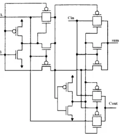
Figure 11. The Full Adder Cell Using MAJORITYNOTNOT Gate.
(PDP) have been measured for full adder circuit and rep-resented in Table 3. The frequency of circuits was
1MHz .In first mode for each floating gate capacitor, 1 Mega ohm resistance is connected in parallel with the capacitor.
In second mode for floating gate transistors, we use Quasi floating gate transistors presented in Figure 2, and in third, fourth and fifth modes, we use Quasi floating gate transistors presented in Figures 3-5.
Due to the problems observed in designing the circuits, the refresh circuits are better to be used on floating gate. However, using these circuits needs more space, whereas the reduction of leakage current would be observed as well at which the advancement of technology and the reduction of gate oxide thickness bring about the prob-lems in the gate leakage. As observed all the refresh cir-cuits, the circuit represented in this paper involves the optimized efficiency of power, speed and gate leakage current. Figure 12 shows this full adder circuit. In
Table 3. The Values of Power, Delay and PDP for Various Modes of Full Adder Circuit in Figure 12.
Mode Power (W) Delay (S) PDP
1 1.8076 × 10⁻⁷ 4.6489 × 10⁻⁸ 8.4033 × 10⁻¹⁵
2 3.5831 × 10⁻⁸ 4.2303 × 10⁻⁹ 1.5157 × 10⁻¹⁶
3 1.4738 × 10⁻⁷ 5.0014 × 10⁻⁹ 7.3710 × 10⁻¹⁶
4 8.7101 × 10⁻⁸ 1.9851 × 10⁻⁸ 1.7290 × 10⁻¹⁵
5 2.6908 × 10⁻⁸ 3.0128 × 10⁻⁹ 8.1068 × 10⁻¹⁷
Figure 12. The full adder circuit.
ad-der circuit in Figure 12 has been shown in Figure 14 which it has been shown with Micro Wind software. The obtained results about measurement of power and delay in this circuit have been reported in Table 4 which it has been concluded that the obtained results were in consis-tent with the results of simulation. Due to the effect of parasitic capacitors in Post layout mode, the difference between the obtained results in this circuit and the ones in simulation are reported.
Figure 13. The inputs and outputs of full adder circuit.
Figure 14. The layout of full adder circuit.
Table 4. The obtained values of power and delay measure-ment in full adder circuit.
Power (w) Delay (s) PDP(j)
3.0829 × 10⁻⁸ 3.4133 × 10⁻⁹ 1.0522 × 10⁻¹⁶
4. Full Adder Cells
There are various structures of full adder cell in various kinds of logics like CMOS, transition gate and pass- transistor logic circuits which are presented in papers and books [12,13]. In this relation, only the circuits with high efficiency were used for comparison and observation.
4.1. The conventional Full Adder with 28 Transistors in CMOS Technology (CCMOS)
The advantage for CMOS logic is the sustainability against sizing the transistor and changing the voltage in which noise increases and this leads to the reliable performance of circuit with low voltages and optimized size of tran- sistor [13,14]. (Figure 15)
4.2. Pass-Transistor Full Adder (CPL)
The other conventional full adder with 32 transistors has been shown in Figure 16. This full adder produces many internal nodes within inverter in order to obtain the out- put. The main difference between pass-transistor logic and CMOS transistor is in a point that source of transis- tors in pass-transistor logic, instead of being connected to voltage supply is connected to the inputs [15].
Figure 15. Conventional full adder.
Transistors
The low power full adder with 14 Transistors has been indicated in Figure 17, based on low power XOR circuit and transition gate, this circuit has been designed [16].
Static power dissipation is the main problem in this circuit [17].
4.4. Full Adder Circuit with 16 Transistors
The other circuit with 16 Transistors has been implemented which it has been shown in Figure 18. [17].
5. Simulation Results
[image:6.595.310.538.352.452.2]The simulations for full adder circuits have been accom- plished in the 65-Nanometer technology via the HSPICE software. Four circuits for simulations have been selected. The main specialty in these circuits was the high effi- ciency in low voltage supply. Simulations were accom- plished in a same condition for all the circuits. The size of transistors was considered as low as possible. The frequency and the environment temperature were con- sidered 1MHz and 25℃. Delay from the moment which input voltage gets to 50% of final value was computed. This value has been measured for all of the decline and as- cent passes by which the maximum values were con-sid- ered as the delay of circuit.
[image:6.595.113.236.413.550.2]Figure 17. Full adder circuit with 14 transistors.
Figure 18. Full adder circuit with 16 transistors. In comparison with other circuits, this circuit com-
pared to CCMOS, CPL and 14T involves less power dis- sipation as 93%, 30% and 93%, respectively. The values of supply voltage (1 volt ) has increased up to 3% for TFA, and has decreased up to 83%, 95% and 94% for CCMOS, CPL and 14T. Simulation results have been represented in Tables 5-7, respectively. As observes, the ratio of efficiency advancement in circuits is more obvi- ous in low supply voltages by which within increase of supply voltage, power dissipation and the multiplication of power by delay increase in these circuits.
6. Conclusions
In comparison with other full adder cells involving high efficiency, the circuit represented in present paper in-volves the most optimized efficiency. As a matter of fact, within the increase of voltage supply, the speed in the circuits increases so that, dissipation power increases as well which this leads to the decrease of efficiency in this
Table 5. The Comparison of Average Power Dissipation, Delay and PDP with Voltage Source = 0.6 V.
The type of full adder circuit
Average of power dissipation
Maximum
delay (s) PDP (j)
CCMOS 4.5092 × 10⁻⁷ 6.1461 × 10⁻⁹ 2.7713 × 10⁻¹⁵
CPL 9.9035 × 10⁻⁷ 8.1457 × 10⁻⁹ 8.0670 × 10⁻¹⁵
TFA 8.2301 × 10⁻⁸ 2.3346 × 10⁻⁹ 1.9213 × 10⁻¹⁶
14T 9.8967 × 10⁻⁷ 5.4395 × 10⁻⁹ 5.3833 × 10⁻¹⁵
[image:6.595.310.539.493.591.2]QFGMOS 6.2017 × 10⁻⁸ 1.3408 × 10⁻⁹ 8.3152 × 10⁻¹⁷
Table 6. The Comparison of Average Power Dissipation, Delay and PDP with Voltage Source = 0.8 V.
The type of full adder circuit
Average of power dissipation
Maximum
delay (s) PDP (j)
CCMOS 5.0610 × 10⁻⁷ 5.9201 × 10⁻⁹ 2.9961 × 10⁻¹⁵
CPL 1.5506 × 10⁻⁶ 7.6898 × 10⁻⁹ 1.1923 × 10⁻¹⁴
TFA 8.7090 × 10⁻⁸ 2.1041 × 10⁻⁹ 1.8324 × 10⁻¹⁶
14T 1.3505 × 10⁻⁶ 5.1562 × 10⁻⁹ 6.8087 × 10⁻¹⁵
[image:6.595.109.235.577.709.2]QFGMOS 7.5169 × 10⁻⁸ 1.3256 × 10⁻⁹ 9.9644 × 10⁻¹⁷
Table 7. The Comparison of Average Power Dissipation, Delay and PDP with Voltage Source=1 V.
The type of full adder circuit
Average of power dissipation
Maximum
delay (s) PDP (j)
CCMOS 5.2805 × 10⁻⁷ 4.0010 × 10⁻⁹ 2.1127 × 10⁻¹⁵
CPL 1.8945 × 10⁻⁶ 7.4870 × 10⁻⁹ 1.4184 × 10⁻¹⁴
TFA 8.8050 × 10⁻⁸ 1.4723 × 10⁻⁹ 1.2963 × 10⁻¹⁶
14T 1.6743 × 10⁻⁶ 4.7254 × 10⁻⁹ 7.9117 × 10⁻¹⁵
[image:6.595.309.538.632.725.2]circuit. As a consequence, Quasi floating gate circuits are a better choice for being used in supply voltages in which the circuit involves threshold voltage, also these circuits on the basis of power dissipation are recommended to be used in this situation. Modern methods are recommenced to design Quasi floating gate circuits by which we could take advantages of floating gate technology while the disadvantages would be decreased.
REFERENCES
[1] A. Bellaouar and I. Mohammad and Elmasary, “Low Power Digital VLSI Design, Circuits and Systems,” Klu-wer Academic Publishers, Norwell, Massachusetts, USA, 1998.
[2] J. T. Kao and A. P. Chandrakasan, “Dual-threshold Tech-niques for Low Power Digital Circuits,” IEEE Journal of Solid State Circuits, Vol. 35, No. 7, 2000, pp.1009-1018.
doi:10.1109/4.848210
[3] J. Alfredsson, S. Aunet and B. Oelmann, “Basic Speed and Powerproperties of Digital Floating Gate Circuits Operating in Subthreshold,”Proceeding of IFIP Interna-tional Conference on Very Large Scale Integration, IFIP VLSI-SOC 2005, Australia , 2005.
[4] J. Alfredsson and B. Oelmann, “Influence of Refresh Circuits Connected to Low Power Digital Quasi–floating Gate Designs,”IEEE International Conference on Elec-tronics, Circuits and Systems, Vol. 1-3, 2006, pp. 1296-1299.
[5] E. R. Villages, “Low Power and Low Voltage Circuit Design with the FGMOS Transistor,” the Institute of En-gineering and Technology, London, 2006.
[6] K. A. Townsend, J. W. Haslett and K. Iniewski, “Design and Optimization of Low Voltage Quasi floating Gate Digital Circuits,” Proceeding of 9th international data-base engineering and application symposium 2005, IDEAS 05, 2005.
[7] A. Bellaouar, I. Mohammad and Elmasary, “Low Power Digital VLSI Design,” 1998.
[8] F. Razaghian and S. Bonakdarpour, “Reducing the Leak-age Current and PDP in the Quasi-Floating Gate Cir-cuits,” Spring World Congress on Engineering and Tech-nology (SCET2012), Xi'an, China, Vol. 1, 2012, pp. 602-605.
[9] J. Alfredsson and B. Oelmann, "Influence of Refresh Circuits Connected to Low Power Digital Quasi-Floating Gate Designs," IEEE International Conference on Elec-tronics, Circuits and Systems, Vol. 1-3, 2006, pp. 1296-1299.
[10] E. S. Sinencio, "Floating Gate Techniques and Applica-tions," Analog and Mixed-Signal Center TAMU, 2010.
[11] E. R. Villegas,”Low Power and Low Voltage Circuit Design with the FGMOS Transistor,” The Institution of Engineering and Technology, London.
[12] K. Navi and K. H. Omid, “Low Power and High Per-formance 1-Bit CMOS Full-adder Cell,” Journal of Com-puters, Vol. 3, No. 2, 2008.
[13] A. Sayed and H. Al. Assa, “Survey and Evaluation of Low-power Full-adder Cells,” in Proceedings of ESA /VLSI, 2004, pp. 332-338.
[14] R. F. Mirzaee, Mohammad, H. M. Hussein and N. Keivan, “High Speed NP-CMOS and Multi-output Dynamic Full Adder Cells,” International Journal of Electrical, Com-puter and Systems Engineering, Vol. 4, No. 4, 2010.
[15] K. Navi, V. Foroutan, M. R. Azghadi, M. Maeen, M. Ebrahimpour, M. Kaveh and O. Kavehei, “A Novel Low-power Full Adder Cell with New Technique in De-signing Logical Gates Based on Static CMOS Inverter,” Microelectronics Journal, Vol. 40, No.10, 2009.
[16] R. Shalem, K. J. Lizy and J. Eugene, “A Novel Low Power Energy Recovery Full Adder Cell,” in Proceedings of Great Lakes Symposium on VLSI, 1999, pp. 380-388. [17] D. Radhakrishnan, “Low-voltage Low-power CMOS Full
![Figure 4. The other Sample of Inverter Circuit Using the Quasi-Floating-Gate Transistor [11]](https://thumb-us.123doks.com/thumbv2/123dok_us/7809724.730088/2.595.124.219.599.686/figure-sample-inverter-circuit-using-quasi-floating-transistor.webp)