5
XI
November 2017
28
©IJRASET (UGC Approved Journal): All Rights are Reserved
A Shared Multiplier for Effectual Area of 1024
Point Fast Fourier Transform Processor
B. Kranthi Sandhya1, B. Ramesh Reddy2, P. Rakesh Kumar3
1
M Tech Student, ECE Department, LBRCE
2
Professor, ECE Department, LBRCE
3
Sr Assistant Professor, ECE Department, LBRCE
Abstract: This paper proposes A Shared Multiplier for Effectual Area of 1024 Point Fast Fourier Transform Processor. This processor utilizes 28% of complex multipliers with reduced area. These processors have flexibility of different Fast Fourier Transform sizes (2, 4,8,16,3,64,128,256 and 512) of length, So that the hardware complexity reduced. The proposed mixed radix butterfly units can be designed in MATLAB SIMULINK. This processors verified by XILINX HDL tool modified with VERILOG language and implemented in 45-nm CMOS technology. The synthesis results shows that area reduce by 19% and achieve a high throughput rate up to 27.5GS/s at 530 MHz In addition, the processor can support for any FFT sizes by addition of stages and works for inverse Fast Fourier Transform by simply taking conjugation of Fast Fourier Transform.
Keywords: Fast Fourier Transform (FFT), Mixed Radix Multipath Delay Commutator (MRMDC), Butterfly Unit (BU).
I. INTRODUCTION
FFT is an important part in OFDM systems.OFDM has been used as a leading modulation technique for wireless and wire line communication standards, such as IEEE 802.11n/ac/ad [1], IEEE 802.15.3.C [2],DAB [3],ultrawide-bandUWB[4], and optical OFDM[5][6].High speed OFDM systems such as wireless personal area networks(WPANS [2], UWB[4] and O-OFDM [5],[6] require high speed FFT computations to meet higher data rates. The FFT Computation of real input samples be in 1-4, gives the symmetry property
of FFT to reduce the computational complexities in different area of applications like medical in electrocardiography [5].
The FFT processors proposed with real time processing requirements and less hardware complexity[9]-[11].To achieves less area, memory based architectures[11]-[14] like application-specific instruction set processors meet the computation of FFT but they cannot reach high-speed requirements. For high throughput rate, There are many pipelined architectures proposed [14]-[16].pipelined architectures are divided into single path delay commutator [14], single path feedback [15],[16],multipath delay feedback or commutator [12]-[14].
The MDC architectures [13]-[15] are a high throughput and used multiple data paths to maintain easy synchronization control. The radix -4 MDC architectures improve the area by reducing of complex multipliers from three to one in each stage. To perform twiddle factor multiplications in one stage leads one clock cycle, another multiplication needs one more clock cycle faster than the system [13]. Therefore, the architecture in [13] may not use as high speed applications. To get high throughput rate, FFT architectures using folding transformations [14], [15] have proposed.
For high speed applications, processors requires a through put rate of over 2 GS/s,radix-8or radix-16 algorithms are used[18].Normally, the FFT size is a power of two, for typical like 128 ,256 ,512 and 1024 FFT sizes are not powers of eight. That is radx-8 algorithms cannot handle these FFT sizes. To provide these requirements, the proposed 1024 FFT processor meets the OFDM requirements by using mixed
Radix algorithm. Therefore the proposed processors can perform FFT computations for sizes of not powers of eight.
A brief interpretation on the128/256,256/512–point MRMDC pipelined FFT processors [17], [18] with eight parallel data paths can operate on high clock frequency. To maintain the demands of OFDM systems, three types MRMDC architectures are proposed [17]. shared multiplier of 1024 -point eight parallel MRMDC FFT processor have Type 1 reduces the number of butterflying units(BU’s in the first stage. Type 2 proposes the shared multiplier of 1024 processor can reduce the complex multipliers for radix-8 BU’s in the second stage. Type 3 combines both the Type 1 and Type 2 can reduce the number of BU’s and complex multipliers.
29
©IJRASET (UGC Approved Journal): All Rights are Reserved
II. MIXED-RADIXFFTALGORITHM
The N-point discrete fourier transform (DFT is defined as X(k) =∑ x(n ) W N nk ,k=0,102,N-1;n=0,1,2,N-1; (1)
Where x(n ) is the input sequence X(k) is the output sequence, and Nis the transform length.WNnk denotes the Nth primitive root of
unity, with its exponent evaluated modulo N and is expressed as WNnk = e-j (2Π nk/N) = cos (2Πnk/N) – sin (2Πnk/N ). (2)
When the FFT size is not a power of radix r, then mixed radix algorithm should be used. For example if
N=256
n = 64n1+n2, 0≤n1≤4,0≤n2≤64
k = k1+4k2, 0≤k1≤4, 0≤k2≤64 (3) Substituting (3) in (1)
X (k) = X (k1+4k2) (4) =∑ x (64n1+n2) W256(64n1+n2) (k1+4k2); 0<n1<4;0<n2<64
=∑ {BF4 (n2, k1)}W64n2k2 ; n2=0,1, . . . . , 63. (5)
The 256 point mixed radix FFT algorithm can be derived from (4) by decomposing the remaining 64-point DFT into 8-point DFT twice.
The MRMDC architecture is explained using 128/256-point MRMDC FFT/IFFT processor [19] .The architecture consists of BU’s, delay commutators, and twiddle factor multipliers. In the first stage, the radix-2/4 BU can perform one radix-4 or two radix-2 operations to compute the 128 and 256-point FFTs. There are three stages based on radix-2, radix-4, and radix-8 algorithms. The input sequence of single path is divided into eight data paths.
III. EXISTING 128-POINT MRMDC FFT/IFFT PROCESSOR
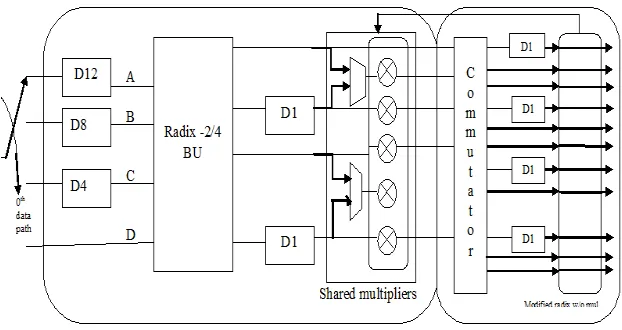
The proposed FFT processor can support the 128-point FFT/IFFT in a similar manner to compute the 256-point FFT described in Section. As shown in Fig. 1, the proposed structure reduces the number of BUs from two to one in the first stage compared with the
existing structure in Fig. 2. In Fig. 2, the input sequence of each data path is split into four data streams, and it takes 12 cycles using D4, D8, and D12 to start the first butterfly computation and four cycles to perform the radix-2/4 operations. To finish the radix-2 computation using one radix-2/4 BU, the proposed structure requires four cycles. Therefore, the first stage of the proposed processor
also requires 16 cycles, even with one radix-2/4 BU. Thus, the structure consisting of one radix-2/4 BU in the first stage can reduce
[image:3.612.155.466.467.632.2]the hardware complexity without increasing the number of clock cycles compared with the existing architecture.
Fig 1: SMSS based 128/256 point FFT Processor
30
©IJRASET (UGC Approved Journal): All Rights are Reserved
(a)
(b)
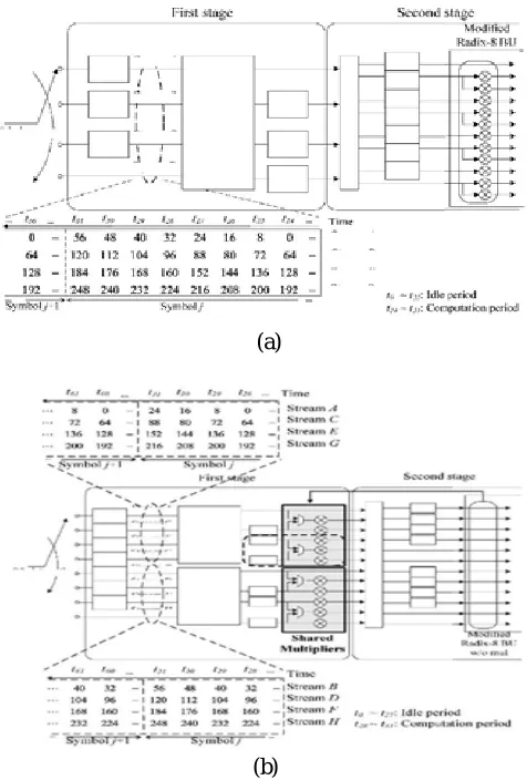
Fig. 3 shows the proposed first stage in the dotted box shown in Fig. 1, which consists of the input buffer, butterfly Processing
element, and commutator. In the first stage, the input sequence of each data path is divided into four data streams (A, B, C, and D), which are delayed by the delay elements to synchronize proper cycles. The butterfly opera- tions in the first stage are performed by
four data streams. The output data of the first stage are delivered to the second stage through the delay elements and the delay commutator by the operation modes.
[image:4.612.186.424.72.424.2](c)
Fig 2: Existing first stage of the zeroth data-path for the 256-point FFT
A. Reducing the number of butterflies (Type I)
B. Reducing the number of complex multipliers (Type II)
[image:4.612.185.428.508.656.2]31
©IJRASET (UGC Approved Journal): All Rights are Reserved
The FFT size determines the delay cycle of each delay element and the butterfly operation of the first stage. Moreover, the switching
of the multiplexers, MUX1, MUX2, and MUX3, depends on the FFT size regardless of whether the data on the same path are to be delayed or not. The control signals of the delay elements vary with the FFT size, and each delay element has different operation modes depending on the FFT size.
D. Second and Third Stage Structure
The input data multiplied by the appropriate twiddle factors are fed into the second stage for the radix-8 butterfly operation through
the delay commutator, as shown in Fig. 2. In the second stage, the remaining radix-8 calculation without multiplications is performed because all the multipliers of the second stage in the existing one are moved to the shared multipliers in the proposed first
stage. A suitable structure is required to ensure the correction of the FFT output data because the third stage in Fig. 1 is different from the second stage. All the output data generated by the radix-8 butterfly in the second stage are fed to the third stage by a
specific order
in3 (p,l) =out2(l, p) (6)
Where in3 and out2 represent the input data of the third stage and the output data of the second stage, respectively. In (13), p and l represent p =0, 1... P−1 and l = 0, 1... L−1, respectively.
P is the number of parallel data paths and L is the number of outputs from a parallel data path.
The proposed processor has the eight-parallel paths, and each path has eight- parallel data streams (A,...,H). The radix-8 BU operates in the third stage using the input sequence from the second stage based on (4). In the existing architecture, the second stage consists of the radix-8 BU in [16] that requires 11 complex multipliers. The third stage using the radix-8 BU also requires 11 complex multipliers. Therefore, the existing architecture requires a total of 22 complex multipliers. In contrast, the proposed architecture requires five multipliers
And 11 multipliers in the first stage and the third stage, respectively. Therefore, the proposed architecture in Fig. 2(c) has 16
multipliers, while the existing architecture requires 22 multipliers for each data path. The proposed MRMDC in Fig. 1 has a total of 128 (16× 8) multipliers because the processors have eight- parallel data paths, whereas the existing architecture requires 176 (22×8) multipliers.
IV. PROPOSED1024POINTFFTPROCESSOR
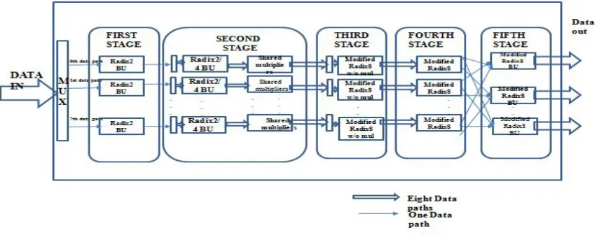
[image:5.612.104.530.486.654.2]This subsection presents the proposed MRMDC 1024-point FFT processor. Fig. 3 shows the proposed processor that consists of four stages. The radix-2 BUs in the first stage are added to support the 512-point FFT compared with that shown in Fig. 1. The second, third, and fourth stages are the same, as shown in Fig. 1. The processor shown in Fig. 4 performs the 1024-point FFT, which is similar to the 256-point FFT in Fig. 2(c). As shown in Fig. 4.
Fig 3: Block Diagram of 1024 –point FFT processor.
The input sequence is split into eight-parallel data paths that are delayed to arrange the input data order in the first stage. Fig. 10
redrawn from the dotted box in Fig. 3 shows one data path of the existing and proposed structures for the 1024-point FFT,
32
[image:6.612.151.473.76.196.2]©IJRASET (UGC Approved Journal): All Rights are Reserved
Fig 4: Structure of the proposed first and second stages of 1024 point FFT processor
The SMSS shown in Fig. 5 can also be applied to the 1024-point FFT. To perform the 1024-point FFT, the proposed structure computes twiddle factor multiplications for the second stage using the shared multipliers on each parallel data path. By employing SMSS, the proposed processor can support both the 256- and 512-point FFTs. In addition, the proposed MRMDC can be applied to larger-size FFTs, such 2048, and 4096, using additional stages. For example, the 2048-point FFT processor consists of one radix-4 BU, the shared multipliers, one radix-8 BU without multipliers, and two radix-8 BUs.
V. RESULTS
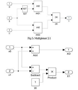
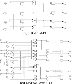
The multiplexer, radix 2, and radix 2/4 and modified radix-8BU can be designed in MATLAB Simulink as shown in figures 4,5and 6.
[image:6.612.156.455.381.723.2]The first and second stage sf the 1024 Point FFT processor is modeled in Verilog with RTL diagram as shown in Fig 9.then that processor operated in the cadence 45 nm technology to perform with high speed compared previous methods in [16],[17].The processor have the form of physical design as shown in fig 11.
Fig 5: Multiplexer 2:1
33
[image:7.612.183.433.75.367.2]©IJRASET (UGC Approved Journal): All Rights are Reserved
Fig 7: Radix-2/4 BU.
Fig 8: Modified Radix-8 BU.
The proposed SMSS based FFT/IFFT processor using Shared multiplier is designed using Xilinx ISE14.2 tool and modeled in Verilog HDL. The proposed FFT processors use shared multiplier to improve computation speed. The synthesis result shows the area efficiency of propose processor and computation speed improvement. The proposed processor is simulated using Xilinx ISim simulator. The Radix Butterflies of processor is done using MATLAB Simulink Tool. SMSS
[image:7.612.179.431.463.708.2]based FFT/IFFT processor implemented using CADENCE 45nm technology by implementing in this technology we reduce area, delay or power.
34
©IJRASET (UGC Approved Journal): All Rights are Reserved
Fig 10: Physical Design of 1024 point FFT processor.
VI. COMPARISONS
Comparison for Hardware Complexities table 1:
Performance Comparison Table 2:
Technology Wise Comparison Table 3:
Expecting that the processor have same throughput rate i.e. (64*clock rate) =36.48GS/s at 570 MHz clock rate. The equipment multifaceted nature and calculation speed are looked at in the execution table. The equipment intricacy is contrasted and the current SMSS based 256-point FFT processor as far as ASIC outline metric door check. The proportional door mean the proposed processor is gotten from the union report of Xilinx XST apparatus. The union report of proposed processor is appeared in figure 7.3.The combination report gives gadget use rundown as far as FPGA plan metric. With a specific end goal to think about regarding door
processor Existing128 Proposed12 8
Proposed 1024 Area(mm2) 11,82,099 3,56,810 20,21,796
Power(uw) 1,41,630.8 8,97,534.5 37,34,251
Timing(ns) 5.30 2.615 1.735 Clock rate (MHz) 188 382 570 Gate count 4,52,634 1,71,804 2,40,43,548 Throughput(GS/s) 1.5 3.056 4.560 TGR 0.0001856 0.0009961 0.000152
Cadence(180nm) Cadence(45nm) Area(mm2) 20,21,796 5,38,660
Power(uw) 37,34,251 20,99,075
35
©IJRASET (UGC Approved Journal): All Rights are Reserved
check, the proportional entryway tally is figured in light of NAND entryways required to configuration cut registers, cut Look Up Tables (LUT's).The timing report gives the data about most extreme clock recurrence, way delay for the proposed processor. The performance comparison is shown in above table 1. From the above data conclusion is that the proposed processor can be performance effective by applying for re-configurability feature and multiplier using optimizes the area and delay for the FFT/IFFT processor.
VII. CONCLUSION
In this thesis report we proposed A Shared Multiplier for Effectual Area of 1024 Point Fast Fourier Transform Processor. This processor utilizes 28% of complex multipliers with reduced area. This processors have flexibility of different Fast Fourier Transform sizes (2,4,8,16,3,64,128,256 and 512) of length, So that the hardware complexity reduced. The proposed mixed radix butterfly units can be designed in MATLAB SIMULINK. This processors verified by XILINX HDL tool modified with VERILOG language and implemented in 45-nm CMOS technology. The synthesis results shows that area reduce by 19% and achieve a high throughput rate up to 27.5GS/s at 530 MHz. In addition, the processor can support for any FFT sizes by addition of stages and works for inverse fast Fourier transform by simply taking conjugation of Fast Fourier Transform.
In addition the proposed architecture can apply any FFT size greater than 256 point using additional stages.
REFERENCES
[1] The Wireless LAN Media Access Control (MAC) and Physical Layer (PHY) Specifications, IEEE Standard 802.11, 2012. [2] Wireless Medium Access Control (MAC) and Physical Layer (PHY) Specifications for High Rate Wireless Personal Area Networks (WPANs): Amendment 2:
Millimeter-wave based Alternative Physical layer Extension, IEEE Standard P802.15.3c/D13, 2008.
[3] IEEE Standard for Local and Metropolitan Area Networks Part 16-Air Interface for Fixed and Mobile Broadband Wireless Access Systems Amendment 2: Physical and Medium Access Control Layers for Combined Fixed and Mobile Operation in Licensed Bands and Corrigendum 1, IEEE Standard 802.16e-2005, 2006.
[4] Radio Broadcasting System: Digital Audio Broadcasting (DAB) to Mobile, Portable and Fixed Receivers, Standard ETSI EN 300 401, Sep. 2000.
[5] DVB, Framing Structure, Channel Coding and Modulation for Digital Terrestrial Television, Standard ETSI EN 300 744 v1.4.1, Jan. 2001. [6] Multi-band OFDM Physical Layer Proposal for IEEE 802.15 Task Group 3a, IEEE Standard 802.15.3a, Mar. 2004.
[6] P.-Y. Tsai, T.-H. Lee, and T.-D. Chiueh, “Power-efficient continuous- flow memory-based FFT processor for WiMax OFDM mode,” in Proc. Int. Symp. Intell. Signal Process. Commun. Syst., Dec. 2006, pp. 622–625
[7] M. Garrido, K. K. Parhi, and J. Grajal, “A pipelined FFT architecture for real-valued signals,” IEEE Trans. Circuits Syst. I, Reg. Papers, vol. 56, no. 12, pp. 2634–2643, Dec. 2009.
[8] J. Huang and S.-G. Chen, “A green FFT processor with 2.5-GS/s for IEEE 802.15.3c (WPANs),” in Proc. Int. Conf. Green Circuits Syst., Jun. 2010, pp. 9–13 [9] X. Guan, Y. Fei, and H. Lin, “Hierarchical design of an application- specific instruction set processor for high-throughput and scalable FFT processing,” IEEE
Trans. Very Large Scale Integer. (VLSI) Syst., vol. 20, no. 3, pp. 551–563, Mar. 2012.
[10] S. He and M. Torkelson, “Designing pipeline FFT processor for OFDM (de)modulation,” in Proc. Int. Symp. Signals, Syst., Electron. Sep. 1998, pp. 257–262. [11] C.-H. Yang, T.-H. Yu, and D. Markovic, “Power and area minimization of reconfigurable FFT processors: A 3GPP-LTE example,” IEEE J. Solid-State
Circuits, vol. 47, no. 3, pp. 757–768, Mar. 201
[12] T. Cho and H. Lee, “A high-speed low-complexity modified radix-25 FFT processor for high rate WPAN applications,” IEEE Trans. Very Large Scale Integer. (VLSI) Syst., vol. 21, no. 1, pp. 187–191, Jan. 2013.
[13] C. Chung, S. Wang, and C. Li, “Area-efficient architectural design of radix-4 pipeline fast Fourier transform processor,” in Proc. Workshop Consum. Electron. Signal Process. Nov. 2004, pp. 1–4.
[14] M. Ayinala, M. Brown, and K. K. Parhi, “Pipelined parallel FFT architectures via folding transformation,” IEEE Trans. Very Large Scale Integer. (VLSI) Syst., vol. 20, no. 6, pp. 1068–1081, Jun. 2012.
[15] M. Garrido, J. Grajal, M. A. Sánchez, and O. Gustafsson, “Pipelined radix-2k feedforward FFT architectures,” IEEE Trans. Very Large Scale Integer. (VLSI) Syst., vol. 21, no. 1, pp. 23–32, Jan. 2013
[16] M. A. Jaber and D. Massicotte, “A new FFT concept for efficient VLSI implementation: Part I—Butterfly processing element,” in Proc. IEEE Int. Conf. Digit. Signal Process. Jul. 2009, pp. 1–6.
[17] Eun Ji Kim ,Jea Hack Lee, “Novel Shared Multiplier Scheduling Scheme For Area Efficient FFT/IFFT Processors” in IEEE Circuits And Systems Society,IEEE Computers Society,IEEE Solid - State Circuits Society,sept,2015.
[18] VLSI Architecture of Shared Multiplier Scheduling Scheme for Reconfigurable FFT/IFFT Processor 1B. Anil Babu, 2V. Sree Lakshmi. IJECT Vol. 7, Issue 3, July – sept 2016, Issn: 2230-7109 (online), ISSN: 2230-9543.
[19] K.-J. Yang, S.-H. Tsai, and G. C. H. Chuang, “MDC FFT/IFFT processor with variable length for MIMO-OFDM systems,” IEEE Trans. Very Large Scale Integer. (VLSI) Syst., vol. 21, no. 4, pp. 720–731, Mar. 2013.
36
©IJRASET (UGC Approved Journal): All Rights are Reserved
1. Author profile
B.KRANTHI SANDHYA, Student in Department of Electronics and Communication Engineering LakiReddy BaliReddy College of Engineering, Autonomous (Affiliated to JNTUK), Mylavaram, pin521230.
Email: [email protected] phone no: 9959223652
2. Author profile
B.RAMESH REDDY, Professor & HOD in Department of Electronics and Communication Engineering. LakiReddy BaliReddy College of Engineering, Autonomous (Affiliated to JNTUK), Mylavaram, pin 521230.
Email: [email protected] phone no: 9440990927
3. Author profile
P.RAKESH KUMAR, Sr.Asst.Professor in Department of Electronics and Communication Engineering. LakiReddy BaliReddy College of Engineering, Autonomous (Affiliated to JNTUK), Mylavaram, pin 521230.