Design of wideband Circular Microstrip Patch
Antenna Using Partial Ground Plane Technique for
UWB Applications.
Manish Parihar1
1
Lecturer, Department of Electronics Engineering, Government Polytechnic College, Jalore,(Raj)
Abstract: In this paper, design of Circular Microstrip Patch Antenna is proposed for Ultra Wide Band Application. Microstrip
feed line of 50Ω characteristic impedance is used to feed the patch. Partial ground plane technique is used to convert narrow
band characteristics of Microstrip Patch antenna into wide band characteristics.FR-4 Epoxy Dielectric Substrate is used for
design havingr= 4.4 and having standard thickness of 1.58mm. The design was optimized by using CST Microwave Studio TM
2011 software to obtain most suitable configuration in terms of desired value of Return Loss, VSWR and Bandwidth for antenna.
Keywords: Circular Microstrip Patch Antenna, Partial Ground Plane, UWB, Bandwidth, Return Loss, VSWR, Gain
I. INTRODUCTION
Now day’s wireless gadgets has become a part of human life. A lot of electrical and electronic devices around us are using wireless system to communicate or operate. Antenna is an essential unit of wireless system which radiates electromagnetic waves into the space by converting electric power given at the input into the radio waves. At the receiver side antenna again receive these radio waves and convert them back into the electrical power[1-2]. Antenna is widely used in cellular phones, smart phones, satellite communications, DTH service, spacecraft, radars, wireless door phones, laptops, tablets and wireless computer networks[3]. Microstrip antennas are perfect for these application as it is light weight and can be easily integrated into antenna arrays or into microwave printed circuit boards. But these have a major drawback of narrow frequency bandwidth[2]. Two days wireless systems works over wide band of frequency[4] and hence the antenna should be capable for the same. In this research, an attempt is made to modify a narrow band antenna to work as ultra wide band antenna. By using techniques like partial ground plane[5], slotting the patch, etc wide band characteristics have been observed[6]. In microstrip antenna, a metallic layer of particular shape is bonded on a dielectric substrate which forms a radiating element and another continuous metallic layer on the other side of substrate as ground plane. Not only the basic shapes but any continuous shape can be used as the radiating patch[7]. For satisfactory performance of antenna VSWR <2 and Return Loss (R.L) < -10dB throughout the entire ultra wide band range[8].
II. DESCRIPTION OF WORK
A narrow band Circular Microstrip patch is designed. Then using partial ground plane technique wide band characteristics is observed by changing the parameters like length, width of antenna and length, width of ground plane.Effect of substrate thickness on return loss and frequency bandwidth has also been observed. Performance Analysis of designed antenna has been optimized in CST Microwave StudioTM 2011 software which utilizesfinite Integration Technique for Electromagnetic Computation[9]
III. ANTENNA DESIGN CONFIGURATION
A. Circular Patch Antenna
Fig. 1 Front and back view of Circular Microstrip Patch Antenna.
[image:3.612.71.538.270.412.2]B. Description of designed antenna
Table 1 represents Dimension of designed Circular Microstrip Patch Antenna
Parameters Description Value(mm)
Lsub Length of substrate 18
Wsub Width of Substrate 12
Lf Length of feedline 7
Wf Width of feedline 2
a Radius of Circular patch 5
Mt Thickness of patch 0.07
h Thickness of substrate 1.58
Lg Length of ground plane 4
IV. RESULT AND DISCUSSION
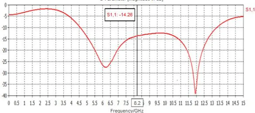
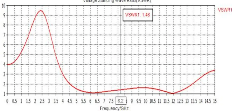
The return loss, VSWR, gain and directivityof designed antenna for resonant frequency of 8.2 Ghzis shown below in Fig 2. (a, b, c, d) respectively .
It is observed thatthe design achieves return loss of -14.26 dB and the bandwidth of 8.43 GHz (4.74 - 13.17GHz) and corresponding VSWR is 1.48. The design antenna have Gain of 3.71 dB and Directivity of 4.58 dB. These results make it suitable for UWB application.
[image:3.612.81.521.522.717.2]Fig. 2(b) VSWR versus Frequency Plot, VSWR =1.48
2D Radiation pattern plot for- Fig. 2(c) Gain= 2.9 dBFig. 2(d) Directivity = 3.6 dB
[image:4.612.67.542.99.327.2]A. Effect of Substrate Thickness on Return Loss, VSWR and Bandwidth:- 1) The results have been tabulated below for ease of understanding.
Table 2 Variation of thickness of substrate
No. Of Iteration
Substrate Thickness
Dielectric Constant
Operating Bandwidth (GHz)
Band width (GHz)
Return Loss (dB)
VSWR
1. 1.4 4.4 4.88-13.10 GHz 8.22 GHz -12.36 dB 1.63
2. 1.58 4.4 4.74-13.17 GHz 8.43 GHz -14.26 dB 1.48
3. 1.65 4.4 4.72-13.17 GHz 8.45 GHz -14.81 dB 1.44
[image:4.612.76.536.625.715.2]2) Return Loss Plot for Various values of Substrate Thickness is shown below in Fig 3
Fig. 3 Return Loss versus Frequency Plot for Various values of Substrate Thickness
(Red Line for h = 1.4mm, Green Line for h = 1.58mm, Blue Line for h = 1.65mm, Purple Line for h = 1.7mm)
3)VSWR Plot for Various values of Substrate Thickness is shown below in Fig 4
Fig.4 VSWR versus Frequency Plot for Various values of Substrate Thickness
(Red Line for h = 1.4mm, Green Line for h = 1.58mm, Blue Line for h = 1.65mm, Purple Line for h = 1.7mm)
From above plot we can say that with increase of substrate thickness, bandwidth of patch antenna increases and value of Return loss and VSWR decreases which indicates that the radiation efficiency and performance of antenna improves with increases of substrate thickness. But it will make antenna bulky.
Thickness of substrate, can also be used for matching between feed line and patch so that maximum power can be transmitted from source to antenna and losses can be minimized.
V. CONCLUSION
[image:5.612.81.537.384.556.2]A. The designed antenna attains return loss of -14.26dB and bandwidth of 8.43 Ghz (4.74-13.17GHz) for resonant frequency of 8.2 Ghz and corresponding VSWR is 1.42. The design antenna have Gain of 2.9 dB and Directivity of 3.6 dB. These above results make it suitable for UWB application.
B. Partial ground plane technique is a simple and effective technique for attaining ultra wide band characteristics.
C. With increase of thickness of substrate, bandwidth of patch antenna increases and value of Return lossVSWR decreases, but it will make antenna bulky.
D. By using thicker substrate and with proper coupling and feeding scheme radiation efficiency of patch antenna minimized.
VI. ACKNOWLEDGEMENT
The above work was carried out by author during his masters at M.B.M Engineering College Jodhpur under the direction of his esteem Prof. & Head (Dr.) V. S. Chauhan, Department of Electronics & Communication Engineering, M.B.M Engineering College Jodhpur. The author expresses his deep indebtedness for his valuable guidance throughout the work. I would also like to thank Mr Kulbhushan Prajapati, Scientist ‘D’ D.R.D.O Jodhpur for his valuable practical & technical support, and encouragement that he gave me from time to time during the preparation of this work.
REFERENCES
[1] C.A. Balanis, “Antenna Theory Analysis and Design”, 3rd Edition, New Jersey, John Wiley and Sons, 200
[2] Ramesh Garg, PrakashBhartie, InderBahl, ApisakIttipiboon, “ Microstrip AntennaDesign Handbook”, pp. b1-68, 253-316 Artech House Inc. Norwood, MA,2001
[3] Sana Ullah, Murad Ali, Md. Asdaquehussain, kyung sup kwak, “Applications of UWBTechnology”, IEEE July 2010
[4] Suhana Rashid, Chandan Kumar Chakrabarty, “Bandwidth Enhanced Rectangular Patch Antenna Using Partial Ground Plane Method For WLAN Applications”. The 3rd NationalGraduate Conference(NatGrad2015), Tenaga National University, Putrajaya Campus, Malayasia ,8-9 April 2015
[5] ParulBansal, EkambirSidhu, Sonia Goyal, “Comparative Study of Notched CircularSlotted and Advances in Engineering and Technology, IJERA ISSN: 2248-9622 , 29th March 2014
[6] AbhishekViswanathan, Rajasi Desai, “Applying Partial-Ground Technique to EnhanceBandwidth of a UWB Circular Microstrip Patch Antenna” IJSER, Volume 5, Issue 10, October-2014, ISSN 2229-5518.
[7] Gary Breed, “An introduction to DGS in Microstrip Circuits”, High frequency Electronics Summit bTechnical Media, LLC, November 2008
[8] Mishra, P. Wankhade and A. Sahu, "Design and analysis of T and U shaped slots with truncated corner rectangular microstripatch antenna for return loss enhancement," 2016Symposium on Colossal Data Analysis and Networking (CDAN), Indore, 2016, pp. 1-7,doi: 10.1109/ CDAN. 2016.757090