F. Cuccureddu, S. Murphy, I.V. Shvets, M. Porcu, H.W. Zandbergen, N.S. Sidorov, S.I. Bozhko
PII: S0039-6028(10)00178-0 DOI: doi:10.1016/j.susc.2010.04.017
Reference: SUSC 18967
To appear in: Surface Science
Received date: 2 February 2010 Accepted date: 21 April 2010
Please cite this article as: F. Cuccureddu, S. Murphy, I.V. Shvets, M. Porcu, H.W. Zandbergen, N.S. Sidorov, S.I. Bozhko, Surface morphology of c-plane sap-phire (α-alumina) produced by high temperature anneal, Surface Science (2010), doi: 10.1016/j.susc.2010.04.017
ACCEPTED MANUSCRIPT
Surface morphology of c-plane sapphire (
α
-alumina)
produced by high temperature anneal
F.Cuccureddu*1, S.Murphy†1, I.V.Shvets1, M.Porcu2, H.W.Zandbergen2, N.S.Sidorov3
and S.I.Bozhko3 1
Centre for Research on Adaptive Nanostructures and Nanodevices (CRANN), School of Physics,
Trinity College, Dublin 2, Ireland
2
National Centre for High Resolution Electron Microscopy, Department of Nanoscience,
Delft Technical University, Lorentzweg 1, 2628 CJ, Delft, The Netherlands
3
Institute of Solid State Physics, RAS, Chernogolovka, Moscow District 142432, Russia
Abstract
A comparative study of the morphological surface evolution of c-plane (0001) α
-Al2O3 upon annealing was investigated for non-miscut (i.e. substrates with 0°
nominal miscut) and vicinal substrates. The samples were annealed in air at 1100°C
for different durations of time. Although non-miscut samples do not show any step
bunching at this temperature, miscut substrates show a regular and ordered stepped
morphology with clearly defined terraces as revealed by Atomic Force Microscopy
(AFM) and Transmission Electron Microscopy (TEM) image analysis. The surface
morphology presents a number of coalescence points, i.e. locations where two steps
merge and form a multiple step. Close to the coalescence points, parallel steps change
direction to different low index direction.
Keywords
Aluminum oxide; Sapphire; Step formation and bunching; Surface structure,
morphology; Atomic force microscopy.
*
Corresponding author: E-mail address: cuccurf@tcd.ie.
† Current affiliation: Center for Individual Nanoparticle Functionality, Building 312, Technical University of Denmark
ACCEPTED MANUSCRIPT
1 Introduction
Alumina is a technologically attractive substrate with applications in electronics,
optics, chemical catalysis and mechanics [1, 2, 3]. The α phase, also called ruby,
corundum or sapphire, is the most thermodynamically stable. This makes α-alumina
an attractive substrate for studies and understanding of metal-oxides. Sapphire has an
hexagonal close-packed crystal structure and belongs to the R-3c space group with
lattice constants a = 0.476 nm and c = 1.299 nm. The crystal structure along the
(0001) direction is composed of an approximately hcp stacking of large oxygen
anions, the separation between two oxygen planes equals 0.21 nm which corresponds
to c/6.
Sapphire single crystals are used as substrates for deposition and the four most
commonly encountered crystallographic planes are essentially: c- (0001), r- (1012),
a- (11-20) and m- (10-10) (Fig.1(a)). In particular c-plane sapphire substrates are
extensively used for the growth of a large range of materials, such as III-V and II-VI
compounds for Light Emitting Diodes (LED) and laser diodes [4], nitrides for surface
acoustic wave materials and wireless communication devices [5], and ZnO for
bandgap devices [6]. Copper, palladium, silver, gold and other metals [7, 8, 9] have
been deposited and studied on c-plane sapphire because the metal-alumina interface
plays an important role in many materials for industrial applications such as catalysts
[10], thermal barrier coatings [11] and microelectronic devices [12].
C-plane sapphire is an optimal template for growing nanowires because of its
capability to provide well-ordered surface steps [13, 14, 15, 16, 17, 18, 19, 20]. The
(0001) surface can have three chemically different surface terminations: an oxygen
surface layer, a surface with two aluminium layers or a surface dissecting between
the two aluminium layers. The latter has been predicted to have the lowest surface
energy from theoretical calculations whilst the oxygen-terminated surface has the
highest surface energy [21]. Several studies have been carried out in order to follow
the surface evolution at high temperature. Using a dynamic scanning force
ACCEPTED MANUSCRIPT
reconstruction was observed [23]. It has also been found that, in addition to the (1×1)
termination, the (0001) surface exists in several ordered phases that can be reversibly
transformed into each other by thermal treatment and oxygen exposure [24]. The
high-temperature phase has been known to be oxygen-deficient [25] with a large
(√31×√31)R±9 unit cell observed by electron [26] and X-ray diffraction [27]. This
superstructure has been demonstrated to promote the self-organization of clusters
grown on its surface [23].
Atomic force microscopy (AFM) provides a powerful technique to study the alumina
surface [13, 14, 15, 16]. Successful investigations of vicinal surfaces of alumina at
the nanometre scale were also performed using high-resolution transmission
microscopy (HRTEM) and reflection electron microscopy (REM) [28, 29, 30].
Annealing of (0001) α-alumina samples for several hours in air produces a
terrace-and-step morphology, consisting of wide terraces (typically several hundreds of nm)
separated by surface steps (typically 1-5 nm) whose height is usually a multiple of c
in height (c=1.3 nm is the unit cell parameter of alumina along the c-axis). The
surface evolution of alumina c-plane in the 1000-1500°C temperature range has been
studied by several groups [13, 14, 16]. Step formation starts at temperatures above
1000°C. It has been found that annealing gives rise to steps up to ~2 nm in height.
Furthermore, annealing at 1400°C for durations of between 10 min and 8 hours leads
to facet nucleation and facet coarsening with a gathering of monosteps forming
multiple steps [31].
Faceting enhances the complexity of the surface evolution of sapphire. Different
processes can be identified during the step growth such as step coalescence, step
decomposition [14], step faceting and step bunching [13, 30]. Step bunching is
interesting because the gathering of steps, due to a step-to-step attractive interaction
at long distances [32], allows the formation of multiple steps with considerable
height. Kurnosikov et al. [15] showed that surface structure resulting from an anneal
is defined not only by the anneal temperature and time but also by the values of
ACCEPTED MANUSCRIPT
their respective influences. Step bunching is expected to be a transient phenomenon
preceding the step faceting and its disappearance rate is related, among other
parameters, to the miscut angle θ: the higher θ, the slower the rate of disappearance
of step bunching [15]. Despite the extensive studies of alumina, very few of them
correlate the surface morphology to the miscut angle.
In this paper we will compare the surface morphology of non-miscut and high miscut
samples upon high temperature annealing. We focus on the step bunched structure
formed as a consequence of the high miscut offset used and show that even at
temperatures as low as 1100°C the use of high miscut samples makes it possible to
obtain a uniform step-and-terrace surface morphology with high multiple steps.
2 Experimental
Samples of c-plane (0001) sapphire were obtained from the manufacturer (MTI
corporation, Richmond, CA, USA). The samples were 10x10 mm wide and 0.5 mm
thick, polished on one side. Two different kinds of substrates were used, one with no
miscut and one with 3° miscut along [1-210], sketched in Fig.1(b). The alumina
samples were then cleaned with isopropanol, methanol and acetone using an
ultrasonic bath, and special precautions were taken to minimize exposure of the
surface to any contamination from the furnace environment by annealing the samples
inside an alumina crucible. They were annealed in air at 1100°C and 1350°C for
different lengths of time. To maximize the temperature uniformity, the furnace ends
were closed with thermal insulating bricks.
The surface structure was characterized by AFM studies performed using a SPM
Solver PRO (NT-MDT, Zelenograd, Moscow, Russia) in tapping mode and ambient
conditions. The topographic images were used for the measurements of the height of
ACCEPTED MANUSCRIPT
TEM studies were performed in a Philips CM30-UT high resolution electron
microscope (point resolution 0.17 nm). This microscope was equipped with a
Schottky emitter and was operated at 300 kV.
Figure 1: Sapphire crystal planes (a) and sketch of stepped vicinal c-plane sapphire
(b).
3 Results and discussion
The behaviour of the alumina surface evolution is quite complex as evident from
publications on the crystallographic orientation of the steps. The (0001) surface of
sapphire was found to facet into a terrace-and-step morphology consisting of (0001)
terraces and steps attributed to the gathering of several c/6 steps, where c=1.3 nm is
the parameter of the alumina unit cell along the c-axis: the hexagonal unit cell of
alumina along the c-axis comprises six layers of oxygen divided by double layers of
ACCEPTED MANUSCRIPT
3.1 Influence of annealing temperature
It has been pointed out that increasing the annealing temperature produces an
increase in the average step height of c-plane sapphire surfaces [14]. Morphology of a
nominally flat (0001) surface after annealing at 1100°C for 12 hours is shown in
Fig.2. A regular terrace-and-step morphology is visible but the terrace edges are
poorly defined. The step height mainly consists of monosteps of 0.2 nm. Further
annealing does not change the average step height. At this stage the temperature is
not sufficiently high for the surface atoms to rearrange and trigger the step bunching:
reported step bunching manifests itself a higher temperatures [14, 15]. We confirmed
this by the results in Fig.3, which shows the morphology of the same substrate
annealed at 1350°C for the period of 8 hours to 20 hours. This results in a step-like
structure with well defined terraces and higher steps.
Figure 2: AFM scan of sapphire (0001) surface with nominally 0° miscut after 12
[image:7.595.150.426.371.679.2]ACCEPTED MANUSCRIPT
Figure 3: AFM topography scan (a) and step profile (b) of (0001) flat sapphire
sample after 8 hours annealing at 1350°C in air.
The resulting terraces are about 120 nm wide with a step height which is a multiple of
0.22 nm, with a maximum height up to 2.4 nm. As can be derived from the average
ratio of terrace width to step height, the surface of the studied sample is in fact miscut
from the (0001) plane by some 0.15°.
Faceting of the surface resulting from formation of multiple and bunched steps is
commonly observed and is being driven by the minimization of the overall surface
free energy. The faceting process is thought to occur as a surface evolution through a
series of distinct stages, beginning with the nucleation and growth of individual
facets, formation of facet domains and coalescence of domains and single facets [31,
33, 34].
3.2 Influence of substrate miscut
A substantial change in morphology arises when the same annealing procedure is
[image:8.595.61.530.57.305.2]ACCEPTED MANUSCRIPT
Fig.4(a) and Fig.4(b) we show two representative AFM scans for a surface with 3°
miscut where the stepped structure of the substrate after 6 hours of annealing in air at
1100°C, is clearly visible. Figure 4(c) shows the profile of the stepped surface of the
[image:9.595.55.529.125.671.2]area presented in Fig.4(b)
Figure 4: Morphology of a surface miscut 3° from (0001) after 6 hours annealing at
1100°C (a and b). Step profile along the line marked in Fig.4(b) corrected for plane
ACCEPTED MANUSCRIPT
The alumina (0001) surface is now completely faceted as a consequence of the
advanced step bunching process. The step-and-terrace morphology extends all over
the sample with high regularity. The bunched macrosteps, whose height is on average
well over c, dominate. Analysis of the AFM images highlighted that step edges are
straight and regularly spaced apart. They run parallel to the [10-10] direction and
perpendicular to the original miscut direction, [1-210]. The stepped structure as
shown in these images is routinely repeatable. A statistical analysis of the step width
distribution was carried out taking a considerable number of steps from several
samples. The results are reported in Fig.5 for both 6 hours and 12 hours annealed
samples. The annealing process performed for 6 hours at 1100°C produces a step and
terrace morphology with an average step height of 1.5 ± 0.5 nm and an average
[image:10.595.56.540.215.554.2]terrace width of 44.2 ± 13.7 nm.
Figure 5: Terrace width distributions after (a) 6 hours and (b) 12 hours annealing at
1100°C.
According to some studies the step edges are not aligned along any low index
crystallographic direction [14] while other studies showed that the annealing of
c-plane sapphire produces a step-and-terrace morphology where the steps follow low
index directions such as [1-210] and [10-10] [15, 35]. This can give rise to zigzagged
ACCEPTED MANUSCRIPT
samples investigated in this paper were chosen to have their miscut direction along
[1-210] in order to facilitate formation of straight and long steps along [10-10] with
the least possible number of kinks. Nevertheless, as shown in Figs.6 and 7, the
annealing procedure provided straight steps at times interrupted by coalescence
junctions, i.e. locations where multiple steps join together forming higher steps.
In the proximity of the merging areas, parallel steps change direction generating
faceting. From analysis of the AFM scans (Fig.6) the angle between the two segments
of step edges at the merging point is around 150°, which corresponds to the angle
between the [1-210] direction and the [1-100] direction. The step edges are
predominantly aligned along [1-210] but in the vicinity of merging steps they change
direction and run along a different low index direction, [1-100] (equivalent to
[10-10]). The formation of higher steps through the coalescence of lower steps follows a
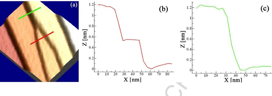
"zipper-like" motion scheme (Fig.7) [14].
Figure 6: Step coalescence provides merging areas forming new facets. The angle
[image:11.595.86.469.335.710.2]ACCEPTED MANUSCRIPT
Figure 7: A 3D close view of a junction (a): the formation of multiple steps follows a
"zipper-like" motion scheme where steps of smaller height join together and give rise
to higher steps. Fig.7(b) and (c) show the step profile along the marked lines in (a):
two steps (red line, (b)) merge "zipping" together to provide a higher multiple step
(green line, (c)).
As reported earlier, the evolution of the (0001) alumina surface morphology follows
several processes including step pairing, coalescence, decomposition, bunching and
faceting [14, 15, 31]. The mechanism of bunching and faceting formation upon
annealing was found to begin with nucleation of single facets followed by the
formation of facet domains and successively by the coalescence of domains and
single facets [31]. At this stage misaligned merging junctions appear on the surface:
the collision of out-of-phase facet domains forms facet junctions with a misalignment
of phase corners. The process continues with the coarsening of facets where the
motion of facet junctions leads to a completely faceted surface, as shown in Fig.6.
The presence of merging steps is then a consequence of the coarsening stage where
the collision of bunched areas causes some portions of steps to deviate locally,
resulting in a change in direction of the step edge to another low-index
crystallographic direction. The concurring phenomena of step bunching and step
faceting make the surface evolution of alumina complicated. Step faceting may start
after the completion of step bunching stage or initiate as the step bunching is still
ACCEPTED MANUSCRIPT
morphology and makes it difficult to separate their respective contributions [15]. The
step edge fluctuation provides a way to lower the overall surface energy during the
surface evolution.
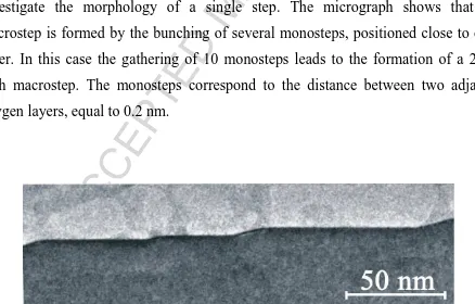
As part of the study, TEM analysis of step morphology was performed. TEM
micrographs confirm the step-and-terrace structure of the samples. In Fig.8 a cross
section view of the sample is shown with the α-Al2O3 represented by the dark area
while the lighter area is the adhesive used in the preparation of the sample for the
TEM analysis. The width of the terraces from the analysis of the TEM micrographs
matches the results of the AFM scans. Fig.9 is a high resolution micrograph of the
alumina sample viewed along [10-10] with the linear arrays of oxygen atoms in
evidence. The crystal structure of alumina is clearly visible and it is possible to
investigate the morphology of a single step. The micrograph shows that the
macrostep is formed by the bunching of several monosteps, positioned close to each
other. In this case the gathering of 10 monosteps leads to the formation of a 2 nm
high macrostep. The monosteps correspond to the distance between two adjacent
oxygen layers, equal to 0.2 nm.
Figure 8: Low magnification micrograph of the alumina sample viewed along
[image:13.595.76.514.340.620.2]ACCEPTED MANUSCRIPT
Figure 9: High resolution micrograph of the alumina sample viewed along [10-10].
A considerable number of theoretical studies are available on the evolution and
motion of step trains. Yet, the origins of this particular kinetic instability are still
debated due to the fact that step bunching can be seen in various physical situations.
The asymmetric kinetic behavior due to the Ehrilch-Schwoebel effect is a possible
cause. Incorporation rates of adatoms from upper and lower terraces differ
significantly and this can generate an instability of the step trains motion during
step-flow growth [36, 37]. Step-step long range interaction was proposed to play an
important role in step bunching. Finally, impurities can interfere with the kinetic
processes and create more complex instabilities [38, 39, 40]. A model proposed by
Frank in 1958 suggested that impurities on the surface can destabilize the uniform
step train during the evaporation (or the crystal growth) impeding the motion of the
step and reducing its velocity [39, 41]. If all the step edges had the same velocity
during the surface evolution, step bunching would not occur. A difference in step
edge velocities is required for bunching and this could be due to the presence of
impurities. In particular, impurities seem to be a likely explanation for the dynamics
of alkali metal halide surfaces where particles present on the surface act as pinning
ACCEPTED MANUSCRIPT
Si etc. affects step and surface structure evolution of alumina samples: the presence
of such impurities forces the steps to bend around them generating mesoscopic
bunching [44]. The initiation of the step bunching process in alumina has been also
related to high levels of K impurities while a combination of high levels of Ca and
low levels of K stabilizes c/6 steps, preventing the bunching itself [20]. These studies
show the sensitivity of alumina c-plane towards different kinds of impurities, the type
of impurity atoms and its quantity can heavily affect the surface evolution.
Accordingly, the annealing environment acquires marked significance as it is
responsible for the adsorption of different kinds of impurities. Our results clearly
suggest that the surface miscut from a low index c-plane undergoes rearrangement of
atomic terraces and forms step bunching more easily than the low index surface. The
rearrangement of a miscut surface takes place at a lower temperature compared to a
non-miscut surface. When comparing our results with results of other publications, it
should be kept in mind that other factors that are difficult to control can also
influence the dynamics of step behaviour. For example, impurities in the sample as
well as the adsorbates related to the annealing environment can have a significant
effect [20].
3.3 Influence of annealing time
At anneal temperature of 1100°C, increasing the annealing time beyond 6 hours does
not seem to produce any further substantial changes in the average step height or the
average terrace width. Fig.10 shows AFM images of vicinal sapphire samples
annealed in air at 1100°C for 12 hours. The samples annealed for 12 hours have an
average step height of 1.8±0.7 nm while the average terrace width is 43.6±14.7 nm
(Fig.5(b)). For practical reasons, the time of the experiment was limited by some
several tens of hours. At the temperature of 1100°C, increasing the annealing time is
not sufficient to provide for mass transport and facet coarsening. Changes in
ACCEPTED MANUSCRIPT
to the fact that bunching is a thermally activated process with a rate exponentially
dependent on the annealing temperature.
Figure 10: Surface morphology of c-plane sapphire after 12 hours annealing at
1100°C.
4 Conclusions
C-plane alumina samples with 0° nominal miscut and 3° miscut along [1-210] were
annealed in air at 1100°C. The surface morphology evolution was then investigated
by AFM and HR-TEM. As most of the work on alumina surfaces focuses on samples
with no miscut, we show that not only temperature and time, but also the miscut
angle play an important role in the surface structure evolution: for samples with a
high miscut the annealing process triggers step bunching at a lower anneal
temperature compared to substrates with non-miscut.
Flat samples, i.e. substrates with 0° nominal miscut, were annealed for various
durations of time at 1100°C and they did not show any step bunching even after long
[image:16.595.57.539.143.519.2]ACCEPTED MANUSCRIPT
too low for the surface atoms to rearrange. This is confirmed by annealing the same
substrates at higher temperatures: in agreement with other studies, and also confirmed
by our experiments, the stepped surface on non-miscut samples can be obtained by
performing the annealing at higher temperatures.
However, as reported, the formation of multiple steps (of height c or higher) due to
step bunching is possible on (0001) alumina only upon annealing at temperatures
over 1400°C. Conversely, we demonstrate that the stepped morphology can also be
obtained by annealing at relatively low temperatures (1100°C) by introducing
substrates with high miscut (3°). The high miscut triggers the instability of the
surface boosting the step bunching process and producing steps several nanometers
high. TEM micrographs gave a closer view of the step bunching and clarify how the
monosteps gather together to form a macrostep. The surface morphology appears
quite uniform on the samples with steps running for several tenths of nanometers.
However, the surface also clearly presents a number of coalescence points, i.e.
locations where two steps merge and form a higher step. Close to the coalescence
points, parallel steps change direction to align along a different low index direction.
The surface morphologies shown here can be a great interest as templates for the
fabrication of ordered arrays of nanowires or nanoparticles on insulating substrates
for various applications [45].
Acknowledgements
The financial support of the Science Foundation Ireland, Contract No. 06/IN.1/I91, is
ACCEPTED MANUSCRIPT
References
[1] P. Dyer, S. Jackson, P. Key, W. Metheringham, M. Schmidt, Excimer laser
ablation and film deposition of Ti:sapphire, Appl.Surf.Sci. 96-98 (1996) 849.
[2] I. Stara, V. Nehasil, V. Matolin, Influence of substrate structure on activity of
alumina supported Pd particles: CO adsorption and oxidation, Surf.Sci. 365
(1996) 69.
[3] T. Minvielle, R. White, M. Hildner, R. Wilson, Temperature dependence of the
epitaxial growth of Pt on basal-plane sapphire, Surf.Sci. 366 (1996) L755.
[4] X. Huang, J. Bai, M. Dudley, R. Dupuis, U. Chowdhury, Epitaxial tilting of GaN
grown on vicinal surfaces of sapphire, Appl.Phys.Lett. 86 (2005) 211916.
[5] T. Suetsugu, T. Yamazaki, S. Tomabechi, K. Wada, K. Masu, AlN epitaxial
growth on atomically flat initially nitrided -Al2O3 wafer, Appl.Surf.Sci 117
(1997) 540.
[6] J. Grabowska, K. Nanda, E. McGlynn, J. Mosnier, M. Henry, Studying the growth
conditions, the alignment and structure of ZnO nanorods, Surf.Coat.Tech 200
(2005) 1093.
[7] K. Luo, X. Lai, C. Yi, K.A. Davis, K.K. Gath, D.W. Goodman, The Growth of
Silver on an Ordered Alumina Surface, J.Phys.Chem.B 109 (2005) 4064.
[8] F. Bock, T. Christensen, S. Rivers, L. Doucette, R. Lad, Growth and structure of
silver and silver oxide thin films on sapphire, Thin Solid Films 468 (2004) 57.
[9] M. Huth, K. Ritley, J. Oster, H. Dosch, H. Adrian, Highly ordered Fe and Nb
stripe arrays on facetted α-Al2O3(10-10), Adv.Funct.Mater. 12 (2002) 333.
[10] B. Gates, Supported metal clusters: Synthesis, structure and catalysis,
ACCEPTED MANUSCRIPT
[11] A. Evans, D. Mumm, J. Hutchinson, G. Meier, F. Pettit, Mechanism controlling
the durability of thermal barrier coatings, Prog.Mater.Sci. 46 (2001) 505.
[12] C. Young, J. Duh, C. Huang, Improved characteristics of electroless Cu
deposition on Pt-Ag metallized Al2O3 substrates in microelectronics packaging,
Surf.Coat.Tech. 145 (2001) 215.
[13] J. Heffelfinger, M. Bench, C. Carter, Steps and the structure of the (0001) α
-alumina surface, Surf.Sci. 370 (1997) L168.
[14] L. Pham Van, O. Kurnosikov, J. Cousty, Evolution of steps on vicinal (0001)
surfaces of α-alumina, Surf.Sci. 411 (1998) 263.
[15] O. Kurnosikov, L. Pham Van, J. Cousty, High-temperature transformation of
vicinal (0001) Al2O3-α surfaces: an AFM study, Surf.Interface Anal. 29 (2000)
608.
[16] O. Kurnosikov, L. Pham Van, J. Cousty, About anisotropy of atomic-scale
height step on (0001) sapphire surface, Surf.Sci. 459 (2000) 256.
[17] M. Yoshimoto, T. Maeda, T. Ohnishi, H. Koinuma, O. Ishiyama, M. Shinohara,
M. Kubo, R. Miura, A. Miyamoto, Atomic-scale formation of ultrasmooth
surfaces on sapphire substrates for highquality thin-film fabrication,
Appl.Phys.Lett. 67 (1995) 2615.
[18] P. Ribic, G. Bratina, Behavior of the (0001) surface of sapphire upon
high-temperature annealing, Surf. Sci. 601 (2007) 44.
[19] K. Simeonov, D. Lederman, Surface structure of (11-20) Al2O3 single crystals
after high temperature annealing, Surf.Sci. 603 (2009) 232.
[20] S. Curiotto, D. Chatain, Surface morphology and composition of c-, a- and
ACCEPTED MANUSCRIPT
[21] S. Blonski, S. Garofalini, Molecular dynamics simulations of α-alumina and γ
-alumina surfaces, Surf.Sci. 295 (1993) 263.
[22] A. de Lozanne, You May Squeeze the Atoms But Don’t Mangle the Surface!,
Science 291 (2001) 2561.
[23] C. Barth, M. Reichling, Imaging the atomic arrangements on the
high-temperature reconstructed α-Al2O3(0001) surface, Nature 414 (2001) 54.
[24] T. French, J. Somorjai, Composition and surface structure of the (0001) face of
α-alumina by low-energy electron diffraction, J.Phys.Chem. 74 (1970) 2489.
[25] M. Gautier, J. Duraud, M. Pham Van, L. Guittet, Modifications of α-Al2O3
(0001) surfaces induced by thermal treatments or ion bombardment, Surf.Sci.
250 (1991) 71.
[26] C. Chang, LEED Studies of the (0001) face of α-Alumina, J.Appl.Phys 39
(1968) 5570.
[27] G. Renaud, B. Villette, L. Vilfan, A. Bourret, Atomic structure of the α-Al2O3
(√31×√31)R±9 reconstruction, Phys.Rev.Lett. 73 (1994) 1825.
[28] Y. Kim, T. Hsu, A reflection electron microscopic (REM) study of α
-Al2O3(0001) surfaces, Surf.Sci. 258 (1991) 131.
[29] T. Hsu, Y. Kim, Structure of the α-Al2O3(11-20) surfaces: facets and
reconstruction, Surf.Sci. 258 (1991) 119.
[30] Y. Kim, T. Hsu, Study of α-Al2O3(1-102)(R) surfaces with the reflection
electron microscopy (REM) technique, Surf.Sci. 275 (1992) 339.
[31] J. Heffelfinger, C. Carter, Mechanisms of surface faceting and coarsening,
Surf.Sci. 389 (1997) 188.
[32] T. Kimoto, A. Itoh, H. Matsunami, Step bunching in chemical vapor deposition
ACCEPTED MANUSCRIPT
[33] C. Carter, J. Heffelfinger, M. Bench, On the faceting of ceramic surfaces,
Surf.Sci. 343 (1995) L1161.
[34] S. Gilliss, A. Altay, J. Reisterer, N. Ravishankar, C. Carter, Monitoring faceting
on ceramic surfaces, Mat.Res.Soc.Symp.Proc. 750 (2002) 379.
[35] D. Susnitzky, C. Carter, Surface morphology of heat-treated ceramic thin films,
Ceram.Soc. 75 (1992) 2463.
[36] R. Schwoebel, E. Shipsey, Step motion on crystal surfaces, J.Appl.Phys. 37
(1966) 3682.
[37] G. Ehrlich, F. Hudda, Atomic view of surface self-diffusion: Tungsten on
tungsten, J.Chem.Phys. 44 (1966) 1039.
[38] M. Sato, M. Uwaha, Morphological instability caused by asymmetry in step
kinetics, Phys.Rev.B 51 (1995) 11172.
[39] N. Cabrera, D. Vermileya, Growth and Perfection of Crystals Wiley, New York
(1958).
[40] J. van der Eerden, H. Muller-Krumbhaar, Morphology and Growth Unit of
Crystals, TerraPub, Tokio (1989).
[41] A. Pimpinelli, J. Villain, Physics of Crystal Growth, Cambridge University
Press, Cambridge, UK (1998).
[42] K. Keller, Observations of the Formation and Kinetics of Surface Steps during
Evaporation and Condensation, Metall.Trans. 22A (1991) 1299.
[43] Z. Munir, Ledgewise Vaporization, Metall.Trans. 22A (1991) 1305.
[44] N. Ravishankar, C. Carter, Bunching of surface steps and facet formation on an
ACCEPTED MANUSCRIPT
[45] F. Cuccureddu, S. Murphy, I. Shvets, M. Porcu, H. Zandbergen, Plasmon
Resonance in Silver Nanoparticles Arrays Grown by Atomic Terrace


![Figure 9: High resolution micrograph of the alumina sample viewed along [10-10]. ACCEPTED MANUSCRIPTA considerable number of theoretical studies are available on the evolution and motion of step trains](https://thumb-us.123doks.com/thumbv2/123dok_us/8801048.914032/14.595.94.501.94.302/resolution-micrograph-accepted-manuscripta-considerable-theoretical-available-evolution.webp)
![Figure 10: Surface morphology of c-plane sapphire after 12 hours annealing at ACCEPTED MANUSCRIPT4 Conclusions C-plane alumina samples with 0° nominal miscut and 3° miscut along [1-210] were annealed in air at 1100°C](https://thumb-us.123doks.com/thumbv2/123dok_us/8801048.914032/16.595.57.539.143.519/surface-morphology-sapphire-annealing-accepted-manuscript-conclusions-annealed.webp)
![[2 Amino 4,6 bis(2 pyridyl) 1,3,5 triazine κ3N4,N5,N6]dichloridocadmium(II)](data:image/gif;base64,R0lGODlhAQABAIAAAP///wAAACH5BAEAAAAALAAAAAABAAEAAAICRAEAOw==)