© 2016, IRJET | Impact Factor value: 4.45 | ISO 9001:2008 Certified Journal
| Page 470
HARDWARE IMPLEMENTATION OF Z-SOURCE INVERTER BASED
DYNAMIC VOLTAGE RESTORER
G.Balasubramanian
11
Assistant Professor, Dept. of Electrical and Electronics Engineering, Arasu Engineering College, Kumbakonam,
Tamilnadu, India
Abstract -The power quality requirement is one of the major issues for power companies and their customers. The analysis of power disturbance characteristics and finding solution to the power quality problems have resulted in an increased interest for power quality. The most concerning disturbances affecting the quality of the power in the distribution system are voltage sag/swell. The DVR is used to mitigate the voltage sag/swell on sensitive load. In this paper presents the hardware implementation of the DVR system with the Z-source inverter (ZSI) working against voltage sag/swell by using dsPIC30F2010 microcontroller. The ZSI uses an LC impedance grid to couple power source to inverter circuit and prepares the possibility of voltage buck and boost by short circuiting the inverter legs.
Key Words:
Z-source Inverter (ZSI), Dynamic
Voltage Restorer (DVR), Voltage Sag, Voltage Swell,
dsPIC30F2010
Microcontroller,
Pulse
Width
Modulation (PWM).
1.
INTRODUCTION
Power quality and reliability in distribution systems have been attracting an increasing interest in modern times and have become an area of concern for modern industrial and commercial applications. Introduction of sophisticated manufacturing systems, industrial drives, and precision electronic equipments in modern times demand greater quality and reliability of power supply in distribution networks than ever before. Power quality problems encompass a wide range of phenomena. Voltage sag/swell, flicker, harmonics distortion, impulse transients and interruptions are a prominent few. These disturbances are responsible for problems ranging from malfunctions or errors to plant shut down and loss of manufacturing capability. Voltage sag/swell can occur more frequently than any other power quality phenomenon. These sags/swells are the most important power quality problems in the power distribution system [1].
Voltage sag or voltage dip is defined by the IEEE 1159 as the decrease in the rms voltage level to 10% - 90% of
nominal at the power frequency for durations of ½ cycles to one minute [2]. The International Electro-technical Commission (IEC) terminology for voltage sag is dip. The IEC defines voltage dip as a sudden reduction of the voltage at a point in the electrical system followed by voltage recovery after a short period from ½ cycles to a few seconds. Voltage sags are usually associated with system faults but they can also be generated by energization of heavy loads or starting of large motors which can draw 6 to 10 times its full load current during starting. Sag durations are subdivided into three categories, instantaneous, momentary and temporary-all of which coincide with utility device operation times.
Voltage swell is defined by IEEE 1159 as the increase in the rms voltage level to 110% - 180% of nominal at the power frequency for durations of ½ cycles to one minute [3]. It is classified as a short duration voltage variation phenomena, which is one of the general categories of power quality problems. The term “momentary overvoltage” is used as a synonym for the term swell. Swells can occur from the temporary voltage rise on the healthy phases during a single-line-to-ground fault. Swells can also be caused by switching off a large load or energizing a large capacitor bank is characterized by their magnitude (rms value) and duration. The severity of a voltage swell is a function of the fault location system impedance and grounding.
© 2016, IRJET | Impact Factor value: 4.45 | ISO 9001:2008 Certified Journal
| Page 471
voltage at its predetermined value. DVR is one the prominent methods for compensating the power quality problems associated with voltage sags/swells. DVR can provide an effective solution to mitigate voltage sag/swell by establishing the appropriate predetermined voltage level required by the loads.
Voltage sag/swell is most important power quality problems challenging the utility industry can be compensated and power is injected into the distribution system. By injecting voltage with a phase advance with respect to the sustained source-side voltage, reactive power can be utilized to help voltage restoration [4].
DVR is one of such power quality device used in power distribution networks. It has lower cost, smaller size and fast dynamic response to the disturbance [5].
The output voltage of the inverter is varied by using different PWM schemes available. Given to the nonlinear nature of the semiconductor devices voltage waveform distortion associated with the high frequency harmonics at the output of the inverter circuit is a common phenomenon. A harmonic filter unit is generally used at the output of the inverter circuit to keep the harmonic distortions at a permissible level. Although the filter unit keeps the harmonic distortion minimum and improves the quality of the generated voltage, it can also introduce voltage drop and phase shift in the fundamental component of the inverter output and needs to be accounted for in the generated compensation voltage [6].
As the quality of power is strictly related to the economic consequences associated with the equipment and should therefore be evaluated considering the customers point of view. So the need for the solutions dedicated to single customers with highly sensitive loads is great since a fast response of voltage regulation is required. Further it needs to synthesize the characteristics of voltage sags/swells both in domestic and industrial distributions [7, 8]. Alongside the variation in magnitudes, voltages sags/swells can also be accompanied by a change in phase angle. This phenomenon is known as phase angle jump (i.e, the variation of phase angle before the onset and during the voltage sag/swell events and is calculated as an argument of the complex voltage) [9].
Passivity-based dynamical feedback controllers can be derived for the indirect stabilization of the average output voltage. The derived controllers are based on a suitable stabilizing “damping injection” scheme [10].
Modern power systems are complex networks consisting of more number of generating stations and load centers which are interconnected through the power transmission lines. There are many issues involved here such as maintenance of the power apparatus in the
system and maintaining the stability of the system operation during fault condition. The power system especially the distribution system, have numerous non linear loads which significantly affect the power quality of power supply. The deviation of voltage, current or frequency which can be described as a power quality problems results in collapse or incorrect operation of customer equipment.
Dynamic Voltage Restorer (DVR) is one of the power electronic devices connected in series to the distribution system. It compensates the voltage disturbances by injecting the voltage of suitable magnitude and phase in series with the line. The DVR, with its excellent capabilities when installed between the supply and the sensitive load, can compensate voltage sag/swell.
2.
DYNAMIC VOLTAGE RESTORER
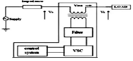
[image:2.595.330.554.538.642.2]Dynamic Voltage Restorer (DVR) is to regulate the voltage at the load terminals irrespective of sag, distortion or unbalance in the supply voltage. The basic operating principle is to inject a voltage of required magnitude & frequency to restore the load voltage under voltage sag or distortion. Generally it employs solid state power electronic switches such as GTO, IGBT or IGCT in the Voltage Source Inverter (VSI) which can be operated in various pulse width modulation techniques such as sinusoidal pulse width modulation, multiple pulse width modulation etc., In normal condition it operates in the standby mode. During the disturbance, the nominal voltage is compared with the voltage variation in order to calculate the voltage to be injected by the DVR to maintain the supply voltage within limits. The DVR is capable of providing the reactive power compensation but the real power is provided by the energy storage system.
Fig. 1: Block Diagram of Dynamic Voltage
Restorer
© 2016, IRJET | Impact Factor value: 4.45 | ISO 9001:2008 Certified Journal
| Page 472
[image:3.595.309.558.109.400.2]fault value. DVR is located downstream of a delta/star transformer. Hence, there is no need to provide zero sequence voltage compensation.
Fig. 2: Location of DVR
2.1
Z-Source Inverter
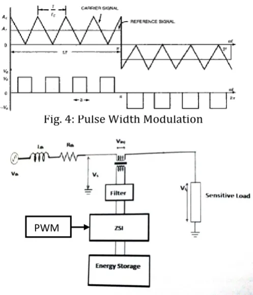
[image:3.595.39.276.152.304.2]Z-source inverter has x-shaped impedance network on its DC side, which interfaces the source and inverter H-bridge. It facilitates both voltages – buck and boost capabilities. The impedance network composed of split inductors and two capacitors. The supply can be DC voltage source or DC current source or AC source. Z-source inverter can be of current source type or voltage source type. Fig. 3, shows the general block diagram of Z-source inverter.
Fig. 3: Block Diagram of Z-Source Inverter
Z-source inverter operation is controlled by multiple pulse width modulation. The output of the Z-source inverter is controlled by using pulse width modulation, generated by comparing a triangular wave signal with an adjustable DC reference and hence the duty cycle of the switching pulse could be varied to synthesize the required conversion. A stream of pulse width modulation is produced to control the switch as shown in the Fig. 4
.
Fig. 4: Pulse Width Modulation
Fig. 5: Block Diagram of Z-Source Inverter with
PWM
2.2
Operating Modes of DVR
Different operating modes of DVR are as follows:
2.2.1 Protection Mode
[image:3.595.42.275.450.556.2]If the over current on the load side exceeds a permissible limit due to short circuit on the load or large inrush current, the DVR will be isolated from the systems by using the bypass switches (S2 and S3 will open) and supplying another path for current (S1 will be closed).
[image:3.595.317.561.583.715.2]© 2016, IRJET | Impact Factor value: 4.45 | ISO 9001:2008 Certified Journal
| Page 473
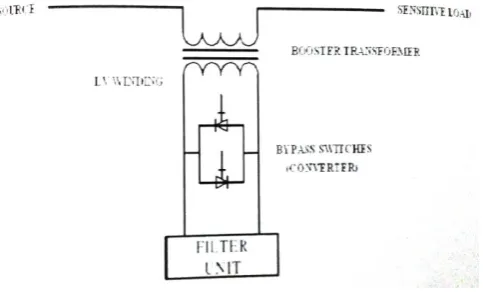
2.2.2 Injection/Boost Mode
In this mode, VDVR > 0. In injection/boost mode the DVR is
injecting a compensating voltage through the booster transformer due to the detection of a disturbance in the supply voltage.
2.2.3 Standby Mode
In this mode, VDVR = 0. The boost transformer low voltage
[image:4.595.318.561.63.232.2]winding is shorted through the converter. No switching of semiconductors occurs in this mode of operation and the full load current will pass through the primary. Losses of the DVR during this mode should be minimized.
Fig. 7: Standby Mode of a DVR
2.3
Control Circuit
Several techniques & control philosophy of the DVR have been implemented for power quality improvement in the distribution system. The DVR is equipped with a control system to mitigate voltage sags/swells. The control of DVR is very important as it involves the detection of voltage sags (start, end & depth of voltage sag) by appropriate detection algorithm. The control strategy can depend on the type of load connected. Its main purpose is to maintain constant voltage magnitude at the point where the sensitive load is connected under system disturbances.
2.4
dsPIC30F2010 Microcontroller
Microcontroller is a highly integrated chip that contains all the components comprising a controller. Typically it includes a CPU, RAM, ROM, I/O ports, Timers and UARTs. Unlike a general-purpose computer, this also includes all of these components. Typically microcontroller is called a dedicated processor that is designed for a very specific task to control a particular system. As a result the parts can be simplified and reduced, which cuts down on production costs. The dsPIC30F1020 microcontroller is
[image:4.595.40.282.284.433.2]several advantages over other microcontroller. Different series of PIC microcontroller are popular because of high performance, low cost, low power consumption and small in size. It uses high performance RISC architecture; PIC16F2010 uses 35 single word instructions having 20MHz operating frequency. The additional flexibility in dsPIC30f2010 microcontroller is that it has 8K X 14 words of flash program memory, 368 X 8 bytes of data memory and 256 X 8 bytes of EEPROM data memory. It also has 8 channel 10 bit ADC, two PWM module, 14 interrupt source, eight level deep hardware stack, direct, indirect and relative addressing modes, power-on reset, power-off timer and oscillator start-up timer, watchdog timer with its own on-chip RC, oscillator for reliable operation, programmable code protection, power saving sleep mode selectable oscillator options, low power, high speed CMOS FLASH/EEPROM technology.
Fig. 8: Pin Diagram of dsPIC30F2010
Microcontroller
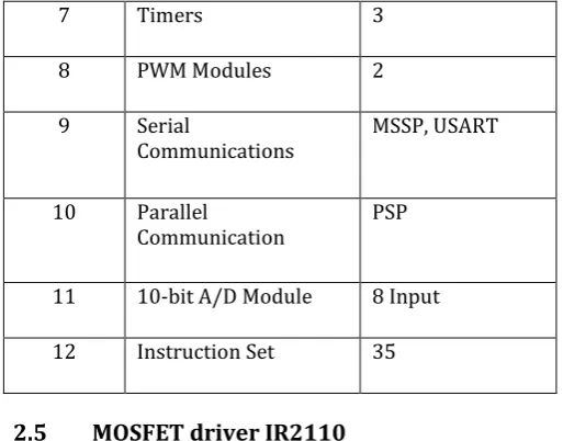
Table – 1: Key features of PIC30F2010 Microcontroller
Serial No. Key Features PIC30f2010
1 Operating Frequency 20MHz
2 Flash Program
Memory 8K
3 Data memory 368 bytes
4 EEPROM Data
Memory 15
5 Interrupts 14
[image:4.595.319.556.310.467.2]© 2016, IRJET | Impact Factor value: 4.45 | ISO 9001:2008 Certified Journal
| Page 474
7 Timers 3
8 PWM Modules 2
9 Serial
Communications MSSP, USART
10 Parallel
Communication PSP
11 10-bit A/D Module 8 Input
12 Instruction Set 35
2.5
MOSFET driver IR2110
The IR2110 is a high voltage, high speed power MOSFET and IGBT driver with independent high and low side referenced output channels. Proprietary HVIC and latch immune CMOS technologies enable ruggedized monolithic construction. Logic inputs are compatible with standard CMOS or LSTTL outputs down to 3.3V logic propagation delays are matched to simplify use in high frequency applications. The floating channel can be used to drive an N-channel power MOSFET or IGBT in the high side configuration which operates upto 6000V.
Fig. 9: Circuit Diagram of MOSFET Driver
Circuit
[image:5.595.41.557.48.767.2]2.6
Hardware Implementation
Fig. 10: Photograph of Hardware
2.7
Hardware Description
[image:5.595.30.287.102.303.2]© 2016, IRJET | Impact Factor value: 4.45 | ISO 9001:2008 Certified Journal
| Page 475
Fig. 12: Power Circuit for Microcontroller
The first building block in the dc power supply is the full wave rectifier. The purpose of the Full Wave Rectifier (FWR) is to create a rectified ac output from a sinusoidal ac input signal. It does this by using the nonlinear conductivity characteristics of diodes to direct the path of the current. The operation of power supply circuits built using filters, rectifiers and then voltage regulators. Starting with an ac voltage, a steady dc voltage is obtained by rectifying the ac voltage then filtering to a dc level and finally, regulating to obtain a desired fixed dc voltage. The regulation is usually obtained from an IC voltage regulator unit, which takes a dc voltage and provides a somewhat lower dc voltage which remains the same even if the input dc voltage varies, or the output load connected to the dc voltage changes.
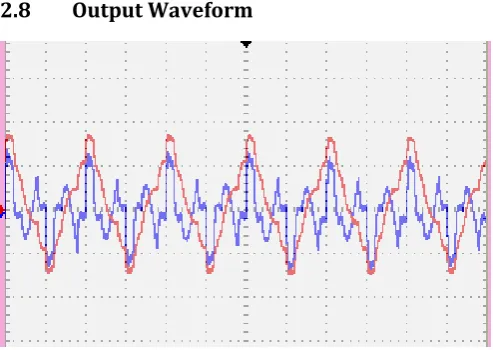
[image:6.595.36.283.310.485.2]2.8
Output Waveform
Fig. 13: Voltage Sag Compensation
Fig. 14: Voltage Swell Compensation
3.
CONCLUSIONS
DVR serves as an effective custom power device for mitigating voltage sag/swell in the distribution system. In case of external disturbances the proposed DVR
handles both balanced and unbalanced situations with sufficient efficiency and accuracy and injects the appropriate voltage component to correct rapidly any deviation in the supply voltage to keep the load voltage constant at the nominal value. Z-source inverter based Dynamic Voltage Restorer to improve the system response and injection capability for the mitigation of voltage sag/swell. In this paper ZSI based DVR with dsPIC30F2010 microcontroller is modeled and the same is installed in the distribution system to provide required load side compensation. Therefore, DVR is considered to be an efficient solution due to low cost, small size and fast response.
REFERENCES
[1] N.G. Hingorani, 1995, “Introducing Custom Power in IEEE Spectrum”, 32p, pp. 41-48.
[2] IEEE Std 1159-2001R, IEEE Recommended Practice for Power Quality Monitoring.
[3] IEC 1000-4-30, “Testing and Measurement Techniques” – Power Quality Measurement Methods.
[4] Choi S. S, Li B. H, and Vilathgamuwa D. M 2000, “Dynamic Voltage restoration with minimum energy injection,” IEEE Trans. Power Systems, Volume 15, pp. 51-57.
[5] Bingsen Wang, Giri Venkataramanan and Mahesh Illindala 2006, “Operation and Control of a Dynamic Voltage Restorer Using Transformer Coupled H-Bridge Converters. IEEE Trans. on Power Electronics. 21:1053-1061.
[6] H. Kim, J. H. Kim, S.K.Sul, 2004, “A Design Consideration of Output Filters for Dynamic Voltage Restorers”, Power Electronics Specialists Conference. PESC 04.2004 IEEE 35th
Annual, Volume6, 20-25 June 2004 page(s):4268-4272 Vol.6.
[7] G. Yalcinkaya, M.H.J Bollen and P.A. Crossely, July/Aug 1998, “Characteristics of Voltage Sag in Industrial Distribution Systems,” IEEE teans. On Industry Appl. Volume 34, no. 4, pp. 682-688.
[8] E.R Collins Jr and S.W. Middlekauff Jan 1998, System and customer impact: Consideration for Series Custom Power Devices,” IEEE Tans. On Power Delivery, Volume 13, no. 1, pp. 278-282.
© 2016, IRJET | Impact Factor value: 4.45 | ISO 9001:2008 Certified Journal
| Page 476
Proc. Generation, Transmission, Distribution, 153: 423-430. DOI: 10.1049/ip-gtd:20050350.
[10] Sira-Ramirez H and Ortega R 1995, “Passivity-based Controllers for the Stablization of DC-to-DC Power Converters,” in Proc. 34th IEEE