OPTIMIZATION OF DEVICES AND LIGHT COUPLING
BASED ON PHOTONIC BIDIMENSIONNELS CRYSTALS
1
RACHIDA. HEDARA, 2AICHA. FLITTI, 1DJAMEL-EDDINE. KALAIDJI
1Telecommunication Laboratory, University Aboubekr Belkaïd Tlemcen
2Faculty of Physics, University of Science and Technology USTO-MB, Algeria,
1[email protected] , 2[email protected]
ABSTRACT
The research high lights the value of using photonic crystals for integrated optics. These materials, whose dielectric constant varies periodically across the wavelength, have the particularity to present photonic bandgap prohibiting light propagation in the structure. The use of this effect bandgap opens the way for the realization of many optical functions such as guide. Usually the guide in photonic crystals is accomplished by creating the linear defects in the lattice constant. Our studies were conducted largely through simulations using executable 2D FDTD software. The choice of the FDTD numerical method (Finite- Difference- Time- Domain) is due to its universality and its simplicity of the use and the implementation. To know the spectral response of this type of periodic as well as field distributions in structures of finite dimensions system, we used the most common 2D FDTD numerical method.
Keywords:Photonics crystals, FDTD, square lattice, waveguide CPs, integrated optical devices, PML.
1. INTRODUCTION
For telecommunications light is a very good vector due to its insensitivity to electromagnetic interference and its high frequency (≈ 1014 Hz) to consider high transmission rates. In addition, the development of optical fibers with low losses makes it possible to transport information over distances of more than 100 km without repeaters. Parallel current technological calendars indicate that the future of microelectronics should be faced with an important technological problem which is the electrical interconnections.
Indeed, the continuation of integration progress may soon face limitations in terms of bandwidth and power dissipation and parasitic capacitances between tracks closer. In addition, the increase in the size of circuits could create problems of synchronization. To overcome this shortcoming, one possibility would be just to use means of optical interconnects. Among the solutions proposed today is the use of photonic crystals.
Photonic crystals are periodic dielectric structures on the scale of the wavelength, with high index contrast. These materials may indeed offer the full range of photons worn by electrons in a crystal lattice behavior: the photon may be banned some energy bands (photonic bandgap) are forced to their energies, slow abruptly.
There is less than a century the concept of BIP structures was developed for the first time by Bragg through the Bragg mirror.
2. GENERALITIES ON PHOTONIC CRYSTALS
In semiconductors, the atomic periodicity prevents the propagation of electrons under certain energies in an area called band gap (gap), and in particular directions [1].
If the crystal potential is large enough, this gap extends to all directions; this is called full bandgap (in the case of semiconductors, which have a complete band gap between the valence band and the conduction band).The optical analogy is the photonic crystal, wherein it has a periodic alternation of macroscopic dielectric materials resulting in a periodic variation of the refractive index. If the dielectric constants of the materials are sufficiently different, and if the light absorption is low, we see, so there have been the same phenomena for photons like electrons in a crystal lattice [2]. The light cannot propagate to certain wavelengths which is called photonic band gap (BIP) [3].
technological advances in microelectronics. Scaling laws to simplify the study of photonic crystals that make non-dependent optical properties of the size of BIP structures [4],[5]. Thus, during
the study of photonic crystals energy bands is usually expressed in terms of standardized factor without dimension u defined by:
u
(1)
a is characteristic size of the photonic crystal (lattice parameter of the crystal), λ the wavelength, ω the angular frequency (rad/s), c is the speed of light in vacuum.
We observe several types of photonic crystals on the number of directions of periodicity: 1D photonic crystal, photonic crystals 2D and 3D photonic crystals (figure1).
2.1 Finite difference time domain algorithm (FDTD)
Maxwell's equations are used to describe the propagation of an electromagnetic wave in a material characterized by its periodic dielectric constant ε.
The optical characteristics of a periodic medium in the case λ ≈ a (a: the period of the photonic crystal) can be obtained from the calculation of own optical modes. The modes are solutions of a wave equation which can be obtained by manipulation of the Maxwell equations.
Maxwell's equations in a nonmagnetic linear dielectric medium, without charge or current are written as:
. ε r E r, t 0 (2)
. H r, t 0 (3)
E r, t μ H r, t (4)
H r, t ε ε r E r, t (5)
Where ε (r) and μ are the dielectric permittivity and the magnetic constant, E and H the electric field and magnetic field vector, r and t space coordinates and time. By manipulating the last two equations, we obtain the following propagation equations for E and H : ! E r, t "# # #H r, t (6)
$ ! H r, t % "# # #H r, t (7)
Fields, E and H can be decomposed into harmonic modes of pulsation ω: E r, t E r e'( (8)
H r, t H r e'( (9)
These equations can be discretized in space and time by a so-called Yee-cell technique. The following FDTD time stepping formulas are spatial and time discretization of equations 1 and 2 on a discrete two dimensional mesh within the x–y coordinate system for the E-polarization [6]: E)∣(,+,- / E)∣(,+,' / / C 1H2 ∣(,+- /, H2 ∣(,+'3 # , H 4 ∣(' / ,+, H4 ∣(- / ,+, 5 (10) H2∣(,+,- H2∣(,+,' / CN(+ E) ∣(,+- /,- / E) ∣(,+' /,- / (11) H4∣(,+,- H4∣(,+,' / CN(+ E) ∣(' / ,+,- / E) ∣(- / ,+,- / (12)
Where the index n denotes the discrete time step, indices i and j signify the discretized grid point in Figure 1: Schematic representation of one-dimensional
the x − y planes respectively. Δt is the time increment, and Δx and Δy are the intervals between two neighbouring grid points along the x and y directions, respectively. Similar equations for the H-polarization can be easily obtained.
It can be easily see that for a fixed total number of time steps the computational time is proportional to the number of discretization points in the computation domain, i.e., the FDTD algorithm is of order N.
The FDTD time-stepping formulas are stable numerically if the following conditions are satisfied [6]:
Δt 8
1 .9:;#3 -:<#3 5
(13)
Where c is the speed of the light.
3. TWO-DIMENSIONAL PHOTONIC CRYSTALS
Two-dimensional periodic structures are periodic in two directions of space and infinite along the third.
Such periodic structures are made of dielectric cylinder. They have a relative geometric simplicity which facilitates the theoretical and experimental studies.
In these 2D structures, there are two possible polarizations for electromagnetic waves. The electric polarization (TE) corresponds to the case
where the electric field E is parallel to the bars of the structure considered infinite length, in the magnetic polarization (TM) , the magnetic fieldH is parallel of infinite cylinders.
3.1 Diagram of bands
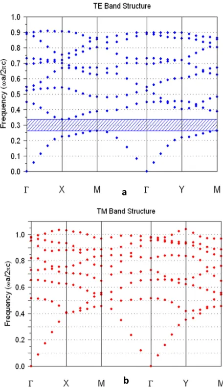
A photonic crystal is characterized by its band diagram. Figure (2) shows band diagrams of a photonic crystal in an engraved substrate of GaAs heterostructure (εsubstrat = 11.4 and εtrou = 1) respectively into TE and TM polarization. These diagrams were calculated by the method of decomposition into plane waves. The fill factor f = 0.30 and the triangular grating of photonic crystal.
A band gap is observed for the TE polarization between u = a / λ = 0.21-0.27 (figure 2. (a)). In
opposite, for the TM polarization, no band gap opens (figure 2. (b)). Indeed, the opening of photonic bands TE is more favored if the areas of high refractive index are connected. Otherwise, if the areas of low refractive index are disconnected (e.g., dielectric pillars in air), is the opening of a bandgap which is favored in the TM polarization [7], [8].
[image:3.595.306.534.303.698.2]Both parameters can be adjusted to play the forbidden photonic band: the refractive index and the air filling factor (the ratio r / a). For a given material (for a given refractive index), it is interesting to know the influence of the factor r / a on the position and width of the photonic gaps: this is the card bandgaps [9].
Figure 2: Diagram of a photonic band crystal (triangular lattice) engraved in a medium dielectric refractive index εsubstrat = 11.4 with a fill factor f = 0.30: (a) TE
polarization; (b) TM polarization.
a
4. THE PHOTONIC CRYSTAL IN GEOMETRY WAVEGUIDE
The development of integrated optics based photonic crystal (PC) through the two-dimensional design and implementation of efficient optical guides. These waveguides are obtained by inserting a line defect in the periodic array 2D triangular. The definition of waveguide photonic crystal indicates the great variety that can cover the term «guide» in CP. Any linear defect can indeed claim to the name «guide» and the parameters, on which we can play, are extremely varied.
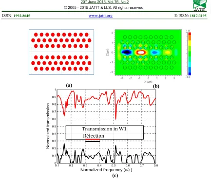
4.1 The single row guide (called W1)
In this section, we are going to interest to the guide along a defect produced in a triangular crystal of air holes when a row of holes is omitted in the direction Г -K of the first Brillouin zone . Such a guide is commonly called a W1 guide. The 2D FDTD simulation gave the Ey electric field distribution and the transmission measurement in TE polarization which are respectively represented in the figure (3.b) and (3.c).
The transmission and reflection coefficients are calculated in respectively πT and πR planes by the Fourier transform of the Poynting vectors obtained for these two positions or by using sensors located in the workspace. This last method consist to calculate the projection of electromagnetic field transverse components E (t) and H (t) on the transverse profiles of normal modes of wave guide strip (Edet, Hdet). Spectrum power transmission T (ω) is written [10]:
T ω
?
@ABC!D+ E 2FGH, I@ABC!D+ JKLM I
/
@ABC!D+ N 2FGH, I
@ABC!D+ OKLM I
P
(14)
Note that in figure (3.c) the transmission extends the frequency range [0.1 0.8] averaged 95 % with a maximum which is the roof of the unit and losses of the order of 2%.
So the losses in the guide of the square structure are significantly higher than the W1 guide triangular structure. The explanation of why these losses are given by the study of structure of the band in a triangular array [11] where in the presence of a large number of bandgap is observed. These PBG, which are numerous in comparison to a square grid,
0.1 0.2 0.3 0.4 0.5 0.6 0.7 0.8
0 0.1 0.2 0.3 0.4 0.5 0.6 0.7 0.8 0.9 1
Normalized frequency (a/λ)
N
o
rm
a
liz
e
d
t
ra
n
s
m
is
s
io
n
4.2 Coupling between lateral guide and
a resonant cavity
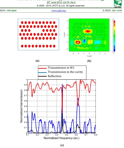
In this section, we study the coupling between the waveguide W1 and a cavity in a two-dimensional photonic grating. The triangular photonic crystal is defined by the following two parameters: lattice parameters a = 500 nm and the fill factor between 35 % and 40 %. These settings allow us to open a wide bandgap approaching 500 nm for TE mode. The structure on which is based this study is shown in figure (4.a). It is a hexagonal cavity corresponding to the omission of a finite photonic crystal holes in the row associated with W1 guide. The cavity and the guide are separated by two rows of air holes.
After the simulation by the FDTD2D, figure (4.c) shows a coupling effect of the guide towards the cavity, in the case where a user is
injected at the input of the waveguide, a portion of the light is extracted to a cavity mode.
We have demonstrated a selective extraction (0.45 and 0.62) guided light.
(c)
Figure 3: (a) Workspace chosen for the FDTD simulation of the guide W1 defined in a square structure (b) Distribution of the electric field Ey when the light is injected
(c) Transmission and reflection spectral responses of the structure W1.
Transmission in W1
Réfection
[image:5.595.84.517.83.455.2](c)
Figure 4: (a) Lateral coupling between W1 guide and a resonant cavity (b) Spatial distribution Ey of the electric field, (c) Transmission and
reflection spectral responses of the structure.
0.1 0.2 0.3 0.4 0.5 0.6 0.7 0.8
0 0.1 0.2 0.3 0.4 0.5 0.6 0.7 0.8 0.9 1
Normalized frequency (a/λ)
N
o
rm
a
liz
e
d
t
ra
n
s
m
is
s
io
n
We have demonstrated a guide coupling effect to the cavity (lateral coupling). In particular, in the case where we inject a mode at the input of the waveguide, a portion of light is extracted to a loss cavity mode. To get this wavelength, we just add to our structure another guide (detection guide) which is identical to the injection guide [12] where the resonance wavelengths in the cavity can be extracted from second guide.
The coupling process depends on the symmetry and also depends on the resonance cavity size; this size must be very well controlled in order to select the desired wavelengths.
This device can be used to perform the routing and multiplexing operations (WDM) / demultiplex wavelength (DWDM).
Transmission in W1
Transmission in the cavity
Reflection
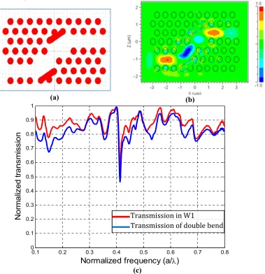
[image:6.595.89.515.79.588.2]4.3 Optimization of a structure with double bends 600
In this section, we consider a double bend obtained by the junction of three identical guides W1 with α angle between them.
The experimental study guide in the dual turns CP was carried out quickly [13], [14], purpose of
reflections and losses problems remain (especially because of the coupling in the double shift modes to leakage in the cone of light).
To avoid the coupling phenomena between propagating modes and turn the bend modes, it is necessary to cancel these reflections by optimizing the reference devices, to improve the transmission
(c)
Figure 5: (a) Selectively coupling two guides W1 and a resonator (b) Spatial distribution of the electric field Ey (c) Transmission and reflection spectral responses of the structure.
Transmission in W1
Transmission in the cavity
Reflection
(a)
[image:7.595.87.503.101.591.2](c)
Figure 6: (a) A double bend of 600 structure (b) Spatial distribution of the electric field Ey
(c) Transmission and reflection spectral responses of the structure.
0.1 0.2 0.3 0.4 0.5 0.6 0.7 0.8
0 0.1 0.2 0.3 0.4 0.5 0.6 0.7 0.8 0.9 1
Normalized frequency (a/
λ
)
N
o
rm
a
liz
e
d
t
ra
n
s
m
is
s
io
n
rate and extend the length of the band wave and reduce losses due to bends.
For this we combine a reflective mirror in the reference curves and we remove a hole at the inner corner; it is therefore obtained by digging a air trench, oriented along the second neighbors, at the elbow tip of the reference curve.
Figure (6.b) gives the intensity of electric field in the structure using the FDTD2D simulator, and
figure (6.c) gives the transmission and reflection spectrums.
After the simulation, the power transmission is about 85% and reflection is equal to 10%, hence a 5% of losses evaluation. We remake improvement in the bandwidth. It is clear that the transmission is almost total in the study range with the presence of some lobes in the double bend which represents losses.
5. CONCLUSION
This work aimed to develop the tools necessary for the design of integrated photonic systems. We are interested in the various building blocks that complete the range of
Transmission in W1
Transmission of double bend
[image:8.595.127.506.260.652.2]
essential elements for the smooth and proper functioning of the optical circuitry. The encouraging results lead us to deepen this research. On the one hand we seek to realize experimentally modeled structures to validate our simulations. On the other hand the continuation of this work will focus on the components in nonlinear integrated optics because the search for new materials for nonlinear optics is known for its best interests represented by the set of non-linear phenomena that result from the action of an electromagnetic wave on the material.
REFERENCE
[1] C.Kittel « introduction to solid-state physics ». 1986.
[2] G.Malpuech, A.Kavokin, G.Panzarini, and A.Di.Carlo « Theory of photon Bloch oscillations in photonic crystals ».Physical Review B 63, 035108 (2001).tel-00341736, version 1 - 25 Nov 2008. [3] E.Yablonovitch « Inhibited spontaneous
emission in solid - state physics and electronics ». Physical. Review. Letters. E (1987) 63: 2059.
[4] K.Sakoda « Optical Properties of Photonic Crystals ».. Vol. 80 of Springer series in optical sciences, Springer, Berlin Heidelberg New York, 2001.
[5] Y.Desiers « Design and optical studies of micro-photonic devices on III-V based materials bandgap structures of photons». Doctoral thesis from the University of Lyon 2001.
[6] M.Qiu.He «Numerical method for computing defect modes in two dimensional photonic crystals with dielectric or metallic inclusions». Physical Review B 61(19), 2000.
[7] J.D.Joannopoulos, R.D.Meade, and J.N Winn «Photonic Crystals, Melding the Flow of Light». Princeton University Press, 1995
[8] W.Barbara « Experimental study of optical properties of crystals and their photonics bidimensionnels accordabillity ». PhD Thesis No. 3573, School Polytechnic Federal of Lausanne, 2006.
[9] M.Zalsmann « Photonic crystals of silicon on insulator for guidance,
filtration, emission and light extraction».
These 7-11 supported the 2003.Université Joseph Fourier- Grenoble1.
[10] F.Raineri « Nonlinear optics in semiconductor photonic crystal III-V». Thesis prepared at the Laboratory of Photonics and Nanostructures - CNRS UPR20 Route Nozay, Marcoussis. [11] M.Bouhenni « Study of a waveguide and
simulation of light propagation in integrated optical structures based two-dimensional photonic crystals». Memoir 2013, University of Djillali Liabes.
[12] S.Noda, A.Chutinan and M.Imada « Trapping and emission of photons by a
single defect in photonic bandgap structure». Nature, Vol 107, pp 608-610, 2000.
[13] T.Bala, N.Fukaya «light wave propagation through à 1200 sharply bent single line defect photonic crystal wave guide». Applied physics letters, 76, 2000. [14] M.Tokushima and H.Hosaka «Light wave