Universal Pattern Set for Arithmetic Circuits
Ashok Kumar
1, Rahul Raj Choudhary
2*, Pooja Bhardwaj
2,
M. S. Dhaka
2, Rajkumar Choudhary
21
Gautam Buddha University, Greater Noida, U.P., India
2
Government Engineering College, Bikaner (Raj) India
ABSTRACT
The exponential increase in test cost is one of the new challenges being posed by technology scaling. This Paper has been aimed to deal with the issue of testing cost which adds to the chip cost. Here we propose a new pattern set for testing the arithmetic circuits which contains a minimum number of test vectors and easy to generate on the chip and hence supports at-speed testing of the circuit. Though maximum fault coverage is desired but practically generation of test vectors for testing of all the possible defects is not at all feasible. This leads to the modeling of defects as faults which facilitate for simplification of test generation process. Though various fault models have been proposed, the single stuck-at fault model is one of widely accepted model because of having closeness to the actual defects and also, it provide the algorithmic possibilities which, further helps in generation of test vectors. The desired smaller DPM (defective parts per million) levels for devices, creates the need for application of better fault models, which can model the defects in the most accurate fashion. This result in complex fault models which tends to make test generation tedious or even impossible and ultimately increase the test cost. Our motive is to cut down the test cost by finding the minimal number of test vectors for the test. If reduction in the patterns for one module is achieved, it would reduce the overall test cost. We propose universal pattern set which gives good fault coverage for arithmetic circuit with small set of vectors.
Keywords
DFT, Universal Pattern Set, Test Cost
1.
INTRODUCTION
CMOS technology scaling has gained tremendous acceleration and conquered new heights during last three decades. Rapid advances in VLSI technology and aggressive design methodologies are resulting into extremely complex devices [1, 2]. Trends in device scaling pose new challenges of reliability and testing. Decreasing CMOS reliability implies that reliability along with performance and power is expected to become a first order design constraint for future high speed digital circuits [3]. The reliability and testing techniques have acquired significant importance in order to achieve a defect free manufacturing and to meet out the expectations of zero failure.
The technology scaling has facilitated an exponential rise in the number of transistors on a single silicon chip. The density has already increased beyond billions of gates resulting in highly complex VLSI circuits. This has made circuit testing a complex and formidable task. The testing cost is exponentially rising and almost touching the design
cost of VLSI chips. However, in addition to this testing cost, costs increased for the loss in the time-to-market and dissatisfied customers due to undetected faults before delivery, can really ruin the future of the manufacturing company. Thus, testing has now attained a position of survival factor for the companies in highly competitive and volatile market.
Arithmetic circuits, comprising Adders and Multipliers are one of the most widely used building blocks in all data processing and digital signal processing. Performance, Area and Power are very important factors that are taken into account while designing modern adders and multipliers. But other than these, in the modern age of scaling, success of design also depends on some critical parameters like testability and ease of design. Arithmetic circuits are regularly used as a main element of data path circuits and their speed seriously affects the performance of the circuit. This is the main reason behind the use of an approach that creates well-optimized designs and these building blocks are optimized in terms of power, area and speed. At-speed testing using an external tester is almost infeasible because of its inherent inaccuracy and cost. The widely used self-testing technique, built-in self-test (BIST), is a structural testing methodology that provides a good quality test. In addition it provides the facility for at-speed testing of the circuit, high fault coverage, and reduced test time for the whole circuit that contains the embedded regular structure which ultimately reduces test cost. This paper is organized as follows: In Section 2, previous work in this domain has been studied. Section 3 discusses the architecture of arithmetic circuits. In Section 4, universal pattern set for arithmetic circuits is explained. In Section 5, experimental results are discussed and Section 6 concludes the paper.
2. PREVIOUS WORK
It is well observed that complexity of modern digital circuits is increasing at very high rate, it demands Built-In Self-Test (BIST) schemes which are necessary for different type of regular structures embedded in complex circuits [4]. The application of effective BIST schemes for regular structures such as embedded parallel multipliers, FIFOs [5], RAMs [6], ROMs [7] etc., gives the above advantages.
Coordination Carry Skip adders, due to their low transistor counts and short wire lengths, dissipate less power than others.
In the complex arithmetic circuits, the implementation of multiplier modules are carried out with two basic approaches i.e. either as tree-like multiplier architecture [10] or as a regular two-dimensional Iterative Logic Array (ILA) [11]. The function of a parallel multiplier can be illustrated in two basic sub-processes where in the first section, the partial products are formulated and the second part deals with creation of the final product of the multiplication by carrying out the sum of these partial products. Effective test patterns can be generated for array multipliers by using regular structures of these multipliers. The widely used types of two dimensional Iterative Logic Arrays (ILAs) are array multipliers which comprise the testability attributes of ILAs. The multipliers may be classified in two categories on the basis of testability. The linear testable class of multipliers have linearly increasing size of test pattern sets with the size of the multiplier operands whereas other class i.e. a C-testable [12], has the constant size of test pattern sets. The Design-for-Testability methods and a comprehensive study of testability of multipliers have been discussed in detail in [13-16] where various fault models of different test pattern set size and variant hardware requirement have been studied. High fault coverage of multipliers is achieved with Cell Fault Model [17]. Such testing is performed with External Tester by applying externally stored test vector sets and further the output response of these multiplier circuits are evaluated and stored externally. Since it is not possible for external testers to operate at rated frequencies of IC, the at-speed testing is not possible with such methods. Since the test vector sets having lower regularity and excessive size, the generation of these test vectors on the chip for BIST is not possible. In such condition, DFT modifications are required for effective reduction of test vector set size. Such modifications degrade the performance of embedded array multipliers. The application of highly regular test patterns which are efficiently generated on the chip without any DFT modifications, for embedded array multipliers, leads to an efficient BIST scheme which leads to a very high fault coverage. BIST designs methods for the Iterative Logic Arrays have been proposed in [18, 19]. A customized Test Pattern Generator (TPG) needs to be designed for the method suggested in [20]. Again, this is applicable only for one-dimensional Iterative Logic Array and further requires modifications to two-dimensional ILAs which increases complexity in hardware. For carry-propagate type array multiplier, test methodology is studied and explained in [18]. Based on the graph labeling techniques, test pattern generation and DFT for Iterative Logic arrays are proposed. Tree multipliers are better choice for performance oriented designs. Testability of tree multipliers is at par with the array multipliers as both of them give the same BIST methodology for testing [17].Tree like parallel multipliers are considered better than array multipliers but due to the lower regularity in their structure, generally avoided for use [10]. The linear programming approach for test pattern generation is proposed in [20] by which the best possible the test vectors are selected from the n-detection test set which is derived out of the weighted defect part level estimation model. The output deviations are used for ranking of patterns in [21].
On the basis of such rankings, the selection of test vector sets, which are in large quantity and time bounded production testing environment is performed.
3.
ARCHITECTURE
OF
ARITHMETIC CIRCUITS
For our experiment we choose following Arithmetic circuits:
1. Ripple Carry Adder (RCA) 2. Carry Look Ahead Adder (CLA) 3. Carry Propagate Multiplier (CPM) 4. Carry Save Multiplier (CSM) 5. Wallace Multiplier
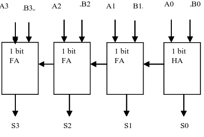
[image:2.595.315.521.279.417.2]Ripple Carry Adder (RCA) is the simplest adder circuit where carry out of previous full adder becomes carry input of next full adder. Due to its simplicity it allows for fast design
Fig. 1 Structure of 4bit Ripple Carry Adder (RCA)
time, but on the other hand the Ripple Carry Adder is slowest as the carry input has to be calculated from previous stage of full adder [22].The CLA, as shown in fig. is used in most of the designs. As compared with ripple carry adder and other adders, CLA is much faster especially in case of larger operands. The carry look-ahead adder is able to generate carries before sum. The carry is produced using propagate and generate logic to make addition much faster but on the other hand it requires additional hardware. The operation of CLA is based on creation of two signals (P and G) for each bit position. P and G are based on whether a carry is being propagated from lesser significant bit position (at least one input should be 1), a carry is being generated in that bit position (both inputs should be 1), or if carry is being killed in that bit position (both inputs are 0). Generally, P is simply the sum output of a half adder and carry output of same adder is G. 1 bit FA 1 bit FA 1 bit FA 1 bit HA A0 B0 A A A A A A A B A A B B S
C C
C C C C
S
C C
S
C C S
C
C C
1 bit FA
1 bit FA
1 bit FA C C
1 bit HA A3 A2 B2 A1 B1 B3 S2
C C
C C C C
S1
C C
S3
Fig. 2 Structure of 4bit Carry Look Ahead Adder (CLA) [22]
The operation of a parallel multiplier is subdivided in two basic sub-processes where in the first section, the partial products are formulated and the second part deals with creation of the final product of the multiplication by carrying out the sum of these partial products. The implementation of first part i.e. formulation of partial products is identical in tree and array multipliers. The difference, between array and tree multiplier, is only the manner in which second part of creation of final product of multiplication is performed. A regular two-dimensional array of full and half adders is used
for creation of final product by array multipliers whereas a tree of full and half adders is used by the tree multipliers for this operation. The Mx × MY multiplier creates Mx
partial products each where each of partial products consists of MY bits. The value of the j
th
bit (j = 0, 1, 2 . . . MY - 1) of the ith partial product (i = 0, 1, 2 . . . Mx - 1) is
obtained by performing AND function of bits Xi and Yj of
the multiplier
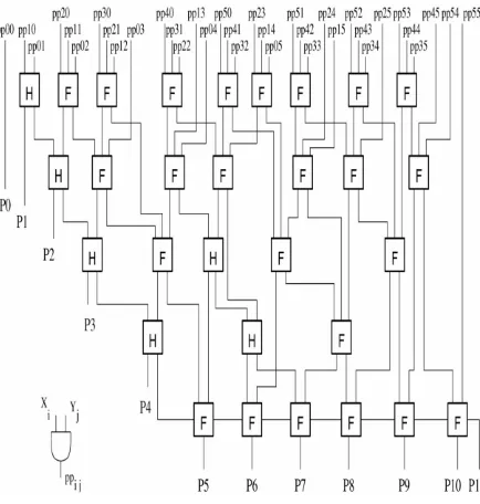
Fig. 3 Structure of 6×6 Carry Propagate Multiplier [17]
and multiplicand respectively. Partial product bits are scripted as ppi. j. A carry-propagate or a carry-save adder
array or a tree structure of adders are used for obtaining the
addition of the Mx partial products which are called carry- propagate array multiplier or carry-save array multiplier or tree multiplier respectively. The 6 × 6 cases for the array multipliers are shown in Figs. 3, 4, respectively, and, for the tree multiplier, is shown in Fig. 5[17].
[image:3.595.317.550.273.612.2]For the case of carry-propagate, at same row, the carry ripples in between the adders while in case of carry-save adder, the addition of carries are performed in the next row. To form final product, the final stage of carry-propagate adder is also mandatory in case of the carry save array multipliers. The rows of both arrays are numbered 0, 1 . . .Mx-1 from top to bottom. The diagonals of full adders are numbered as 0, 1 . . .Ny - 3 from right to left. 2-input AND gates, producing the ppi.j values, of Nx × Ny in numbers are required [17].
[image:3.595.51.285.441.690.2]Tree multipliers, using carry-save configuration, require the carries to be saved for the next stage and in addition these requires the final carry propagation stage. The configuration has been shown in Fig. 5 [17].
Fig. 5 Structure of 6×6 Wallace Multiplier [17]
4. UNIVERSAL PATTERN SET
Universal Pattern set are based on the transition of bits and pattern. It covers all the possible transitions from one test vector to another test vector from left to right, right to left. It also covers all possible transition inside the test pattern. Possible test patterns for 4bit arithmetic circuit are as follows:
Test Pattern 1: 0000 0000, Test Pattern 2: 0000 1111, Test Pattern 3: 1111 0000, Test Pattern 4: 1111 1111, Test Pattern 5: 0101 0101, Test Pattern 6: 1010 1010, Test Pattern 7: 0101 1010, Test Pattern 8: 1010 0101, Test Pattern 9: 0101 0000, Test Pattern 10: 0101 1111, Test Pattern 11: 1111 0101, Test Pattern 12: 0000 0101, Test Pattern 13: 1010 0000, Test Pattern 14: 1010 1111, Test Pattern 15: 1111 1010, Test Pattern 16: 0000 1010.
These are the patterns that we have find as a universal set as these patterns give high fault coverage (average 95%) with minimum number of patterns is 16 for arithmetic circuits. Benefit of these pattern set is that they are uniform in nature so easy to generate on chip with small amount of hardware by using only two bit counter we can generate these patterns.
5. EXPERIMENTAL RESULTS
Universal pattern set consists of only 16 test vectors which give good fault coverage for the arithmetic circuits. For ripple carry adder circuits we achieve 100% fault coverage and for other circuits we are getting fault coverage more than 95% except the Wallace multiplier circuit. In the previous work [17], the average fault coverage obtained through 16 test vectors is 81% while by with only 16 test patterns, we are achieving 95% fault coverage and these test patterns are easier to generate on the chip by using the two bit ring counter only. The result of each circuit are Tabulated as follows-
Table 1: Experimental Results of Universal Pattern Set on Ripple Carry Adder
Size of Ripple Carry Adder (RCA)
Stuck faults
Transient faults
4 bit RCA 100.00% 99.53%
8 bit RCA 100.00% 97.56%
16 bit RCA 100.00% 97.87%
Table 2: Experimental Results of Universal Pattern Set on Carry Look Ahead Adder
Size of Carry Look Ahead Adder (CLA)
Stuck faults
Transient faults
4 bit CLA 100.00% 96.36%
8 bit CLA 94.28% 91.57%
12 bit CLA 96.88% 94.87%
16 bit CLA 89.04% 85.06%
Table 3: Experimental Results of Universal Pattern Set on Carry Propagate Multiplier (CPM)
Size of Carry Propagate Multiplier (CPM)
Stuck faults
Transient faults
8 bit CPM 95.06% 91.49%
16 bit CPM 95.12% 89.88%
[image:4.595.308.528.237.309.2]24 bit CPM 94.89% 88.72%
Table 4: Experimental Results of Universal Pattern Set on Carry Save Multiplier (CSM)
Size of Carry Save Multiplier
(CSM)
Stuck faults Transient faults
8 bit CSM 95.06% 91.49%
16 bit CSM 95.12% 89.88%
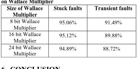
[image:4.595.310.529.346.435.2]Table 5: Experimental Results of Universal Pattern Set on Wallace Multiplier
Size of Wallace Multiplier
Stuck faults Transient faults
8 bit Wallace
Multiplier 95.06% 91.49%
16 bit Wallace
Multiplier 95.12% 89.88%
24 bit Wallace Multiplier
94.89% 88.72%
6.
CONCLUSION
As chip cost is increasing and design cost is almost near to test cost and reduction in test cost reduces the chip cost. Universal pattern set for the arithmetic circuits has minimum number of pattern set and give high fault coverage. By reducing the number of test vectors for single module on the chip reduces the test cost of the chip which ultimately reduces the test cost. As the number of patterns are less in universal pattern set so they are easy to implement on the chip.
7.
REFERENCES
[1] N. Weste and K. Eshragian, “Principles of CMOS VLSI Design”, A Systems Perspective, second ed. Addison-Wesley, 1994.
[2] M. L. Bushnell and V. D. Agrawal, "Essentials of Electronic Testing for Digital, Memory and Mixed-Signal VLSI Circuits", Springer, 2000.
[3] J. A. Rivers and P. Kudva. “Reliability Challenges and System Performance at the Architecture Level”. IEEE Des. Test, 26(6), pp. 62-73, 2009.
[4] V.D. Agrawal, C.J. Lin, P. Rutkowski, S. Wu, and Y. Zorian, “Built- In Self-Test for Digital Integrated Circuits”, AT&T Technical J.,pp. 30-39, Mar./Apr. 1994.
[5] Y. Zorian, A.J. Van de Goor, and I. Schanstra, “An Effective BIST Scheme for Ring-Address Type FIFOs”, Proc. IEEE Int'l Test Conf., pp. 378-387, 1994.
[6] B. Nadeau-Dostie, A. Silburt, and V.K. Agarwal, “Serial Interfacing for Embedded Memory Testing”, IEEE Design & Test of Computers, vol. 7, no. 2, pp. 52-63, Apr. 1990.
[7] Y. Zorian and A. Ivanov, “An Effective BIST Scheme for ROMs”, IEEE Trans. Computers, vol. 41, no. 5, pp. 646-653, May 1992.
[8] T.F.Ngai, M.J.Irwin and S.Rawat, “ Regular area-time efficient carry-look-ahead adders, “Journal of parallel & distributed computing, volume 3, no.3,PP.92-105,1986,
[9] Nuno Roma and Tiago Dias and Leonel Sousa, “Fast Adder Architecture: Modeling and Experimental Evaluation, R.Alves Redol,9, 1000-029 Lisbon, Portugal.
[10] C.S. Wallace, “A Suggestion for a Fast Multiplier”, IEEE Trans. Computers, vol. 13, pp. 14-17, Feb. 1964.
[11] K. Hwang, “Computer Arithmetic: Principles, Architecture and Design”. New York: Wiley, 1978
[12] A.D. Friedman, “Easily Testable Iterative Systems”, IEEE Trans. In Computers, vol. 22, no. 12, pp. 1,061-1,064, Dec. 1973.
[13] J.P. Shen and F.J. Ferguson, “The Design of Easily Testable VLSI Array Multipliers”, IEEE Trans. Computers, vol. 33, no. 6, pp. 554- 560, June 1984. [14] A.R. Takach and N.K. Jha, “Easily Testable Gate
Level and DCVS Multipliers”, IEEE Trans. Computer-Aided Design, vol. 10, no. 7, pp. 932-942, July 1991.
[15] A. Chatterjee and J.A. Abraham, “Test Generation for Arithmetic Units by Graph Labeling”, Proc. FTCS 17, pp. 284-289, Pittsburgh, Pa., July 1987.
[16] S.J. Hong, “The Design of a Testable Parallel Multiplier”, IEEE Trans. Computers, vol. 39, no. 3, pp. 411-416, Mar. 1990
[17] Dimitris Gizopoulos, Antonis Paschalis and Yervant Zorian, “An Effective Built-In Self-Test Scheme For Parallel Multipliers”, IEEE Transactions On Computers, Vol. 48, No. 9, September 1999.
[18] A. Chatterjee and J.A. Abraham, “Test Generation, Design-for- Testability and Built-In Self-Test for Arithmetic Units Based on Graph Labeling”, J. Electronic Testing: Theory and Applications, vol. 2, pp. 351-372, 1991.
[19] E.M. Abdoulhamid and E. Cerny, “Built In Testing of Unilateral Iterative Arrays”, IEEE Trans. Computers, vol. 33, pp. 560-564, June 1984.
[20] Y. Tian, M. Mercer, W. Shi, and M. Grimaila. “An optimal test pattern selection method to improve the defect coverage”. In Proc. of IEEE ITC, 2005. [21] Z. Wang and K. Chakrabarty. “An efficient test
pattern selection method for improving defect coverage with reduced test data volume and test application time”. In Proc. of IEEE Asian Test Symp. 2006, pages 333–338.
![Fig. 2 Structure of 4bit Carry Look Ahead Adder (CLA) [22]](https://thumb-us.123doks.com/thumbv2/123dok_us/8124158.795031/3.595.317.550.273.612/fig-structure-bit-carry-look-ahead-adder-cla.webp)