A Single-Chip UHF RFID Reader Transceiver IC
*
Runxi Zhang, Chunqi Shi, Zongsheng Lai
Institute of Microelectronic Circuits and Systems, East China Normal University, Shanghai, China Email: [email protected]
Received April 2013
ABSTRACT
A single-chip UHF RFID reader transceiver IC has been implemented in 0.18 μm SiGe BiCMOS technology. The chip includes all transceiver blocks as RX/TX RF front-end, RX/TX analog baseband, frequency synthesizer and I2C with fully-compliant China 800/900 MHz RFID draft, ISO/IEC 18000-6C protocol and ETSI 302 208-1 local regulation. The normal mode receiver in the presence of −3 dBm self-jammer achieves −75 dBm 1% PER sensitivity. The linear class-A PA integrated in transmitter has 25 dBm OP1 dB output power for CW. The fully-integrated fractional-N fre-quency synthesizer is designed based on MASH 1-1-1 sigma-delta modulator and 1.8 GHz fundamental frefre-quency LC-VCO for lower in-band and out-of-band phase noise. The measured phase noise is up to −106 dBc/Hz@200 kHz and −131 dBc/Hz@1 MHz offset from center frequency and the integrated RMS jitter from 10 kHz to 10 MHz is less than 1.6 pS. The chip dissipates 330 mA from 3.3 V power supply when transmitting 22.4 dBm CW signal and the PAE of linear PA is up to 26%. The chip die area is 16.8 mm2.
Keywords: Integrated Circuit; Reader Transceiver; Single-Chip; UHF RFID
1. Introduction
UHF RFID reader constructed by discrete components has achieved major market in many applications such as logistic, traffic distribution, asset management and in-dustrial flow line controlling using non-battery-powered system [1]. With the rapid growth of mobile internet ser-vice, we hope UHF RFID readers can be integrated into portable devices such as smartphone, PDA and tablet PC. UHF RFID systems use low data rate less than 640 kbps and simple coding schemes like FM0 and miller [2], the digital baseband signal processing can easily be realized using popular ARM-based processor. The integration scheme of UHF RFID reader transceiver is becoming the critical problem and attracting lots of research attention from all over the world [3-6,12].
This paper describes a monolithic UHF RFID reader transceiver for mobile RFID application, which is fabri-cated in the mature and low-cost 0.18 μm SiGe BiCMOS process. The chip includes all transceiver blocks as low- noise and linear RX/TX RF front-end, configurable RX/ TX analog baseband, sigma-delta modulator (SDM) frac-tional-N frequency synthesizer, linear Class-A PA and some necessary serial interface. The integrated UHF RFID reader is compliant with China 800/900 MHz RF-
ID draft [7], ISO/IEC 18000-6C protocol [8] and ETSI 302 208-1 local regulation [9]. In LBT mode, the RX sensitivity is −85 dBm; in normal mode, while the in- band self-jammer of supplying energy to passive tag is
−3 dBm, the 1% PER RX sensitivity is about −75 dBm. The reader transmitter sufficiently meets the transmission mask of China draft and ISO/IEC 18000-6C multiple- interrogator mode and the out-of-emission requirements from ETSI 302 208-1 regulation. This paper is organized as follows. In Section 2, we will discuss the reader tran- sceiver system architecture. The circuit implementation is described in Section 3. Section 4 will review mea- surement results. Finally, we will give a conclusion in Section 5.
2. System Architecture
Figure 1 shows a block diagram of the proposed UHF RFID reader. Through adding small amount of discrete components as RF circulator, antenna, TCXO, protocol controller and data convertor, the reader can realize iden-tification of passive tags. Because some components such as TCXO, data convertor and controller can be shared with smartphones, the transceiver can easily be adopted for those mobile devices with UHF RFID functions. The RX RF front-end operates in 840 to 960 MHz and per-forms frequency down-conversion. The TX front-end rea-lizes the frequency up-conversion with the help of digital
*This paper is funded by National Science & Technology Major
domain Hilbert filter and supports three regulated mod-ulations of DSB-, SSB- and PR-ASK for dedicated ap-plications. The RX and TX baseband realizes filtration and application of the desired signal. The SDM fraction-al-N frequency synthesizer supply clean LO carrier for frequency translation. The integrated PA is used to ampl- ify signal to the maximum allowed power for saving ex-ternal PA and reducing cost. The high-linearity of PA is helpful in reducing spectrum regrowth in transmitter and meeting transmission mask requirements. The basic chip setting including channel bandwidth selection, operation frequency calibration, DC offset removal and band gap trimming are all configured through I2C interface.
3. Circuit Implementation
3.1. Receiver
[image:2.595.60.290.316.416.2]Because the backscattered signal from tags using FM0 or
Figure 1. Block diagram of the proposed UHF RFID reader.
Miller and containing no DC component, the I/Q di-rect-conversion architecture is adopted in RX path. The I/Q architecture is also helpful in coupling with zero phenomenon of amplitude-modulated signal [3]. The most challenging problem with UHF RFID reader design is the unwanted CW leakage from TX to RX in order to energ-ize passive tags. Accompanying with this problem, the receiver must face the correlated amplitude (AM) noise and phase (PM) noise [10]. Assuming the transmitted power is up to 20 dBm [7], the isolation of circulator (or directional coupler) is up to 22 dB [11], the CW leakage will be 0 dBm level or more [3,4]. For various applica-tions, people mainly adopt two methods of cancellation [12] and accommodation [3-6] to deal with it. In com-parison, the former needs more auxiliary digital algo-rithms and RF power consumption, more likely to be used by fixed readers, the latter is usually adopted by mobile readers. Figure 2 shows the proposed front-end schematic consisting of transconductance, switching stage and transimpedance (TIA). The linearity of RF front-end is very important to accommodate the un-wanted while necessary leakage signal, so low current-efficiency and high output impedance transconductor stage and current- mode passive down-mixer is adopted in RF front-end. The small input impedance of TIA assures the low vol-tage swing before and after switching svol-tage. Because the backscatter signal power is always located around DC, especially for low down-link rate, the lower input-re- ferred noise is a critical design target for high-sensitivity
Figure 2. Schematic of the proposed RX RF front-end.
MOBILE DEVICE Gm TIA DCOC DCS PA PLL DnMIXER UpMIXER CIR
Balun CSFVGA
IRF VGA I/Q I/Q BIAS I2C MUX ADC MUX DAC
UHF RFID READER TRANSCEIVER
Vinp Vinn C1 R1 TP1 VB1 TP2 R2 C2 R5 R6 CMFB C3 R3 TN3 Vref TN4 R4 C4 Cpar Cpar C7 C8 R7 R8 VB2 TN5 TN6 TN7 TN8 TN9 TN10 TN11 T12 R9 R10 C9 C10 Cf Rf Cf Rf Cf Rf Cf Rf Vdd VL0 VL180 VL90 VL270 Vioutp Vioutn Vqoutp Vqoutn I Channel Q Channel VB3 R11 R12
Transconductance Switching Stage Transimpedance
Av
Av
[image:2.595.63.533.447.720.2]565
reader. In addition to AM and PM noise from transmitter, the self-noise of RX RF front-end is contributed by tran-sconductance and operational amplifier (OP-amp) of TIA. We shall trade-off between noise, linearity and conver-sion gain of RF front-end to select appropriate transcon-ductance. We use low flicker noise lateral PNP transis-tors as input devices of OP-amp for better noise perfor-mance. In fact, the input-referred noise contributed by OP-amp is also related with the switching stage parasitic capacitance, the size of switching transistors should be chosen carefully. The designed RF front-end features a SSB-NF of 18 dB, input P1dB of 6 dBm and conversion gain of 10 dB. In order or to be immune from PM noise of TX leakage, we take same signal source with TX lea-kage as receiver LO.
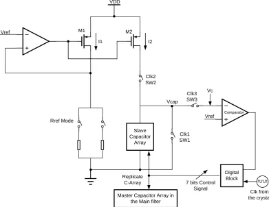
Due to different transmit power and TX-RX isolation, the down-mixer will produce sub-1V DC-offset and sa-turate following stage. The RX analog baseband is pre-ceded by a DC-offset removal circuit which is designed with fast DC-offset cancellation progress and low receive SNR deterioration. A 8th-order Butterworth type active- RC filter provides channel selection and amplification with 4 - 60 dB gain range and 10 dB gain step and 0.25 - 1.35 MHz variable bandwidth. The filter cut-off frequency is calibrated by automatic frequency tuning (AFT) circuit for PVT variation. The adopted AFT scheme is illustrated
in Figure 3, it will share precise 19.2 MHz with external TCXO. The AFT accuracy is up to 3.2% and the calibra-tion time is less than 3 uS.
3.2. Transmitter
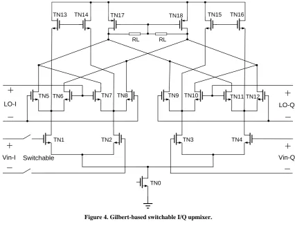
[image:3.595.101.493.414.716.2]The transmitter uses Cartesian direct up-conversion ar-chitecture for DSB-, SSB- and PR-ASK modulations. It is comprised of TX variable gain amplifier, anti-aliasing low-pass filter, DC shifter circuit, up-mixer and on-chip linear PA. The analog signal is filtered by I/Q 6th-order active-RC filter to attenuate DAC output image and sam-pling clock noise. The filter output noise should be re-duced as low as possible because it will be up-converted to carrier frequency in transmitter and deteriorate receiv-er noise floor through TX to RX leakage. The TX varia-ble gain stage ranged from −14 dB to 10 dB with 1 dB step is used to fine-tune TX baseband output amplitude for ACPR performance of transmitter and be fit for va-riant DAC output. According to [2], the reader should support 80% - 90% modulation depth for various appli-cations, a DC shifter circuit without affecting desired sig-nal is introduced between asig-nalog baseband and up-mixer. The circuit can supply up to 0.5 V DC difference in dif-ferential line and implement the required modulation depth for DSB-ASK. A linear Gilbert-based I/Q double- balanced up-mixer with DC-independent load and cur-
Figure 3. Scheme of AFT adopted in RX filter.
Slave Capacitor
Array
Digital Block
Master Capacitor Array in the Main filter
Clk from the crystal 7 bits Control
Signal Replicate
C-Array Rref Mode
Clk1 SW1
Clk3 SW3
Vref Vc VDD
Clk2 SW2 Vref
Vcap
Comparator
I1 I2
rentbleeding transistors is adopted to take the baseband output signal. As shown in Figure 4, the switchable in- phase path combining with DC shifter circuit can
[image:4.595.83.510.143.470.2]imple-ment the regulated SSB-ASK and PR-ASK. The designed up-mixer has a conversion gain of 0dB and output P1dB of 3 dBm. Figure 5 shows a schematic of the class-APA
[image:4.595.84.515.467.720.2]Figure 4. Gilbert-based switchable I/Q upmixer.
Figure 5. Linear class-A power amplifier.
TN13 TN14 TN17 TN18 TN15 TN16
RL RL
TN5 TN6 TN7 TN8 TN9 TN10 TN11 TN12
TN1 TN2 TN3 TN4
TN0 VDD
LO-I
Vin-I Vin-Q
LO-Q
Switchable
CTRL1 VCC1 VBIAS2 CTRL2
VBIAS1
RFIN_N
RFIN_P
VCC2
567
with differential input and single-ended output. The inte-grated balun supplies −5 dB attenuation for assuring sta-ble linear operation. A 10.16 μm × 0.9 μm × 128 vertical SiGe NPN with optimized rectangle-type layout acts as output power-cell. The PA using double-bondpad fea-tures a 25 dBm OP1dB with 37% PAE from 3.3 V power supply. The deep-nwell is used to isolate on-chip PA with other circuits on die.
3.3. Frequency Synthesizer
The SDM fractional-N frequency synthesizer shown in Figure 6 integrates all blocks including PFD, CP, 1.8 GHz constant kVCO double-switch LC-VCO with
capaci-tor and varaccapaci-tor array, 8/9 dual-modulus divider, P/S counter, 20-bit 3rd-order MASH 1-1-1 SDM and I/Q pres-caler except for loop filter components. An AFC circuit with 4-bit output is included for automatic sub-band se-lection in PLL while the tuning time is about 23 uS. The LC- VCO using 2.5 V LDO supply has frequency range from 1.44 to 2.18 GHz and FOM of −186.8.
4. Measurement Results
The single-chip UHF RFID reader transceiver IC is im-plemented 0.18 μm SiGe BiCMOS process, the die ph o-tograph is shown in Figure 7. The die size is 16.8 mm2 and packaged into QFN64. All signal paths are differen-
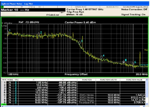
tial to be immune from coupling noise. Figure 8 shows the measured phase noise performance from specified VCO test pins, the carrier phase noise will be 6 dB lower. The spot phase noise is −106/−130 dBc/Hz at 200 kHz/ 1MHz offset from center frequency. The RMS jitter from 10 kHz to 10 MHz is less than 1.6 pS. When transmitting 22.4 dBm and 80 kbps modulated signal, the transmis-sion power is −45 dBc at adjacent channel and −58.2 dBc at alternative channel, it sufficiently meets the transmis-sion mask for multiple-interrogator environments. The measured sensitivity of receiver with 1% PER criterion is
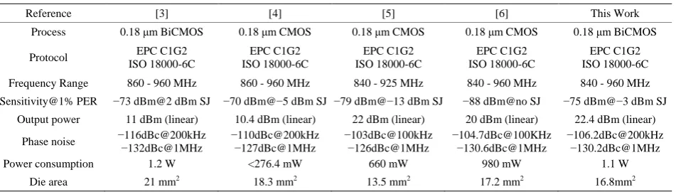
−75 dBm in the presence of −3 dBm leakage at RX input port. The chip dissipates 330 mA from 3.3 V power supply when transmitting 22.4 dBm CW. Table 1 com-pares the measured performance with some state-of-the- art counterparts.
5. Conclusion
[image:5.595.62.540.425.716.2]According to the demand of portable RFID, a single-chip UHF RFID reader is presented in this paper. It integrates all building blocks of transceiver and is fully compliant with China draft, ISO/IEC 18000-6C protocol and ETSI 302 208-1 regulation. In normal mode, it consumes 1.1W when transmitting a 22.4 dBm CW signal and sufficient- ly meets the multiple-interrogator ACPR requirement. With a few added discrete components as directional
Figure 7. Chip microphotograph.
[image:6.595.58.542.366.711.2]569
Table 1. Performance comparison of the existed UHF RFID reader transceiver.
Reference [3] [4] [5] [6] This Work
Process 0.18 μm BiCMOS 0.18 μm CMOS 0.18 μm CMOS 0.18 μm CMOS 0.18 μm BiCMOS
Protocol EPC C1G2 ISO 18000-6C
EPC C1G2 ISO 18000-6C
EPC C1G2 ISO 18000-6C
EPC C1G2 ISO 18000-6C
EPC C1G2 ISO 18000-6C
Frequency Range 860 - 960 MHz 860 - 960 MHz 840 - 925 MHz 840 - 960 MHz 840 - 960 MHz
Sensitivity@1% PER −73 dBm@2 dBm SJ −70 dBm@−5 dBm SJ −79 dBm@−13 dBm SJ −88 dBm@no SJ −75 dBm@−3 dBm SJ
Output power 11 dBm (linear) 10.4 dBm (linear) 22 dBm (linear) 20 dBm (linear) 22.4 dBm (linear)
Phase noise −−116dBc@200kHz 132dBc@1MHz
−110dBc@200kHz
−127dBc@1MHz
−103dBc@100kHz
−126dBc@1MHz
−104.7dBc@100KHz
−130.6dBc@1MHz
−106.2dBc@200kHz
−130.2dBc@1MHz Power consumption 1.2 W <276.4 mW 660 mW 980 mW 1.1 W
Die area 21 mm2 18.3 mm2 13.5 mm2 17.2 mm2 16.8mm2
coupler and antenna and sharing TCXO, protocol control-ler and data convertor with mobile devices, it can easily be used for portable devices needing UHF RFID applica-tions.
REFERENCES
[1] K. Finkenzeller, “RFID Handbook,” John Wiley, 2006.
[2] EPCglobal Inc., “EPC C1G2 UHF RFID Protocol for Communications at 860-960MHz,” Version 1.2.0, 2008.
[3] S. Chiu, et al., “A 900MHz UHF RFID Reader Tran-sceiver IC,” IEEE Journal of Solid-State Circuits, Vol. 42, No. 12, 2007, pp. 2822-2833.
[4] W. T. Wang, et al., “A Single-Chip UHF RFID Reader in 0.18 μm CMOS Process,” IEEE Journal of Solid-State Circuits, Vol. 43, No. 8, 2008, pp. 1741-1751.
[5] L. Ye, et al., “A Single-Chip CMOS UHF RFID Reader
Transceiver for Chinese Mo bile Applications,” IEEE Journal of Solid-State Circuits, Vol. 45, No. 7, 2010, pp.
1316-1327.
[6] J. Kim, et al., “A True Single SoC for UHF Mobile RFID Reader,” Proceedings of IEEE ESSCIRC, Helsinki, 12-16 September 2011, pp. 171-174.
[7] MIIT, “800/900MHz RFID Tech. Draft,” No. 205, 2007.
[8] “ISO/IEC RFID 18000-6,” 2nd Edition, December 2010. [9] ETSI 302 208-1 Technical Requirements and Methods of
Measurement, Version 1.1.1, 2004.
[10] J. Y. Jung, et al., “A Novel Carrier Leakage Suppression Front-End for UHF RFID Reader,” IEEE Transactions on Microwave Theory and Techniques, Vol. 60, No. 5, 2012, pp. 1468-1477.
[11] “MAFRIN0332 Datasheet,” Version2.