VHDL Design of a Scalable VLSI
Sorting Device Based on
Pipelined Computation
Enzo Mumolo , Gabriele Capello and Massimiliano Nolich
DEEI, University of Trieste, Italy Neonseven, Sgonico, TS, Italy
This paper describes the VHDL design of a sorting algorithm, aiming at defining an elementary sorting unit as a building block of VLSI devices which require a huge number of sorting units. As such, an attempt was made to reach a reasonable low value of the area-time parameter. A sorting VLSI device, in fact, can be built as a cascade of elementary sorting units which process the input stream in a pipeline fashion: as the processing goes on, a wave of sorted numbers propagates towards the output ports. In the description of the design, the paper discusses the initial theoretical analysis of the algorithm’s complexity VHDL behavioural analysis of the proposed architecture, a structural synthesis of a sorting block based on the Alliance tools and, finally, a silicon synthesis which was also worked out using Alliance. Two points in the proposed design are particularly noteworthy. First, the sorting architecture is suitable for treating a continuous stream of input data, rather than a block of data as in many other designs. Secondly, the proposed design reaches a reasonable compromise between area and time, as it yields an A T product which compares favourably
with the theoretical lower bound.
Keywords: sorting algorithms, VLSI algorithms, VHDL
language, scalability, pipeline computation.
1. Introduction
The sorting of a series of numbers is a very important task, which embraces many different applications, from banking 18], signal
process-ing techniques, such as order statistics, non lin-ear filtering 24, 8]to communication switching
systems 25, 26]to image processing 7, 13]or
pattern recognition techniques 5, 11].
In this paper the VHDL design of an elementary sorting unit is presented. The main contribu-tion of this paper is to describe a case study of
a simple and general approach to VLSI sorting device. The main goals of the design are to get a low value of the A T product via a simple and regular sorting architecture which requires a moderate silicon area and to arrange the sorting function in a cascaded structure to extend the sorting capability of the device. The main char-acteristics of the design are reported hereafter. The sorting of data is performed according to the value of a key that accompanies the data. The architecture presented in this paper man-ages 16 bit keys and 16 bit data; a technique for upsizing the data field is presented. The key field can be represented with any type of number representation, i.e. unsigned, two complements or floating point; however, in the architecture described in this paper, we consider unsigned 16 bit keys. Both ascending and descending ordering can be implemented in the proposed architecture. Furthermore, any number of in-put words can be managed and, if the number of input words exceeds a threshold related to the internal configuration of the device, some external memory is required.
func-tion using only two registers, one comparator and two output buffers. In view of its character-istics, the sorting block presented here is suit-able for designs which require a huge number of sorting devices, such as, for example, appli-cations in switching systems or in high energy physics.
Other algorithms, namely the algorithms be-longing to the network sorting class, can be more efficient from a computational point of view, but they are less versatile. The well known Batcher algorithm 4, 10, 15, 16], for
exam-ple, is faster than the proposed algorithm for an equal size of input data, but it requires a much larger number of comparators and, should we want to modify the size of the input data, a new design of the sorting device would be under-taken. The proposed algorithm, instead, leads to a scalable architecture and the system can be expanded simply by adding many sorting de-vices in cascade or in parallel. Other VLSI sort-ing algorithms that rely on a simple and mod-ular organization have been presented over the past years, including the compare-swap-based sorting 17], a sorting network-based hardware
sorter 23], the rebound sorter 1, 2], the parallel
enumeration sort 29]and the VLSI sorter 21].
The design presented here, however, has a more modular architecture than the cited algorithms.
The organization of this paper is as follows. In Section 2 the proposed algorithm is described and theoretically analyzed. In Section 3 the architectural design of the sorting device is de-scribed using VHDL pseudo-code, and Section 4 reports of the structural synthesis of the VLSI sorter performed with Alliance, together with the silicon synthesis with the Alliance tools. Fi-nally, Section 5 is devoted to the final remarks and conclusions.
2. The Sorting Algorithm
In this section we give a detailed analysis of the algorithm. In order to prepare for this analysis, it is worth describing very briefly some basic issues related to the sorting problem.
2.1. Basic Issues of the Sorting Problem
Because of its practical importance, as well as its theoretical interest, the sorting problem has been studied extensively in the past 14]. In
computer terminology, sorting is the process of rearranging, in ascending or descending order, a set of values stored in contiguous memory lo-cations. Generally speaking, sorting algorithms can be performed in a serial or a parallel fash-ion. Each of the two classes can lead to Internal and External algorithms, the first making use of internal memory and the second of some kind of external memory. Serial algorithms, moreover, use some approaches to make the sorting task efficient, and can be based on counting, inser-tion, exchanging, selecinser-tion, merging and distri-bution of data 14]. The time complexity lower
bound of serial algorithms is O(N ln N) where
N is the size of the input data1. External algo-rithms, on the other hand, try to use the external device efficiently. Parallel sorting, instead, is based on the parallelism of the operations. The main research problem in this area is to develop algorithms whose performance reaches the the-oretical lower bound, that is a time complex-ity of O(ln N)with an O(N)-processors parallel
machine.
The silicon area of a VLSI circuit is one of the principal cost-related factors involved in the fabrication of the circuit. Generally speaking, the area required by the circuit is related to the logic size and to the modularity of the archi-tecture. Another very important factor is the speed of the circuit. As far as a VLSI sorting algorithm is concerned, however, other figures become relevant, such as the trade-off between the chip area and the sorting time 28, 27].
To compare different VLSI algorithms and ar-chitectures for sorting, it is of great interest to take a look at the lower bounds of area or speed, in the sense that we cannot solve a given VLSI problem using less than a lower bound of silicon area, or in less than a given amount of time. Be-cause of the trade-off between area and speed, it is also important to consider lower bounds of the product A T, or of A T2 28]. If kln N,
where k represents the number of bits in a word and N is the number of input words, well known
1
lower bounds for any sorting VLSI circuits are given in(1):
A=Ω(N)
A T =Ω(N ln N) (1)
A T2 =Ω(N 2
)
In many cases these bounds are weak, in the sense that circuits as good as the bounds re-ported in (1) do not appear to exist; in
gene-ral, the strongest of these bounds is the product A T2.
The earliest VLSI sorting algorithms were de-rived from commonly known serial algorithms 27]. A number of different approaches for
parallel sorting developed afterwards, such as the odd-even merge rule 14, 9]and the bitonic
merge network 22], which are based upon
sort-ing network approaches 4, 14]. The odd-even
transposition sort 14], for example, is a parallel
version of the well-known bubble sorting algo-rithm. It sorts a list of N items by performing N=2 global iterations that involve a comparing–
exchanging step on even and odd pairs of list items in parallel. Some results concerning re-duction of the complexity of the processing ele-ments of a sorting network have been reported in 6, 12].
2.2. Description of the Proposed Algorithm
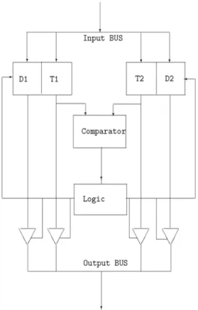
The actual design we describe takes into ac-count the fact that usual applications require the sorting of data to be performed according to the value of a key that accompanies the data. With this assumption, an SU is made up of two registers, one for the data and one for the key. Besides, each SU consists of two sides sharing the same architecture and a control logic which, in its basic form, implements a three-state ma-chine: Reset, Shift&Read1 and Shift&Read2 states. Assuming an ascending ordering, dur-ing Reset the contents of the registers are set to zero. Moreover, during Shift&Readx the con-tents of the key and data registers are passed to the output and a new value is read in it. The structure of a SU is reported in Fig. 1.
A sorting device is made out of a cascading of SUs, thus leading to a scalable architecture. Each SU shares its input bus with the output bus of the previous one and shares the output
Fig. 1. Block diagram of the sorting unit.
The boxes called “D1” and “T1” represent the data and the key registers respectively, the “Comp.” box is the comparator and
the “Logic” box contains the control logic of the unit.
Reset
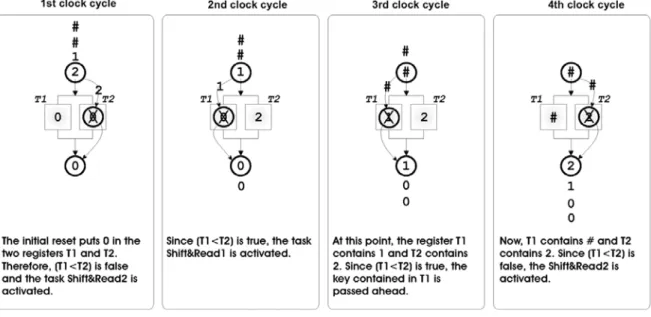
for each clock cycle do { if (T1<T2)
Shift&Read1 else
Shift&Read2 }
Fig. 2. Pseudocode of the sorting algorithm
for ascendig ordering.
bus with the input bus of the next one. The algorithm performed by an SU is described in Fig. 2.
In Fig. 3 an example of sorting the sequence of keys(21) is shown. From this figure, we
Fig. 3. Sorting example of a couple of keys with 1 SU.
The delimiter symbol # represents a number greater than all the keys in the sequence.
2.3. Complexity Analysis
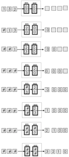
In Fig. 4 another sorting example is shown with a couple of cascaded SUs. From Fig. 4, we would come out with the observation that the sequence of data passing through a single SU is equal to the sequence obtained with one pass of the popular “Bubble Sorting” algorithm applied on the same input. That is, the result of a single sorting unit processing a stream of data is the same as that of the exchanging pass of the bub-ble sort. In the following, we will use the term run for the operations required for processing a block of N input data; for example the Bubble Sort consists of(N;1)runs.
Hence, we can use some classical solutions to our problem. The first solution is described in the following classical Theorem 14].
Theorem 1. Let a1a2:::an be a
permuta-tion and let b1b2:::bn be the
correspond-ing inversion table. If one pass of the bubble sort changes a1a2:::an to the permutation
a0 1a
0
2:::a 0
n, the corresponding inversion
ta-ble b0 1b
0
2:::b 0
n, is obtained from b1b2:::
bnby decreasing each non zero entry by 1.
Therefore, we can say that if a stream of data passes through a sorting unit, each non zero ele-ment of the relative inversion table is decreased by 1. Since each non zero inversion table ele-ment can be, at max,(N;1), we can conclude
that:
Proposition 1. A cascade of (N ;1)sorting
units realizes a complete ordering of a N-long data sequence.
According to 14], the execution time Teof the
bubble sort algorithm can be represented with
Te =K1A+K2B+K3C+K4 (2)
where A is the number of runs, B the number of exchanges and C the number of comparisons and K1:::K4represent the implementation
as-pects, respectively. That is, the coefficients de-pend on the actual code which implements the algorithm and on the instruction timing char-acteristics of the machine on which the code is running. The average and the worst cases’ com-plexities of the Bubble Sort are O(N
2
+N)and
O(N 2
+N ln N)respectively.
The execution time of the proposed algorithm is, instead, given by
Te =K1A+K4 (3)
since the exchanges and comparisons are per-formed parallelly with the input of the data at each clock cycle. In (2), the K4 coefficient
keeps track of the constant execution times and K1 is related to the counterpart of the number
Fig. 4. Sorting example of 3 keys with 2 SU.
The delimiter symbol # represents a number greater than all the keys in the sequence. The rectangles marked in bold denote the T1 and T2 registers. In each rectangle, T1 and T2 are in the lower and upper position respectively.
is the number of times that all the N input data pass through the first sorting unit.
Let us call the number of sorting units U, and assume that U =(N;1)and that the input data
block is N-sized. In general, since A=(N;1),
we have K1 =
N
U and K4 = 2U. In
conclu-sion, the computational complexity, in terms of the number of clock cycles, of a cascade of U = (N;1)sorting units with a N-long input
data sequence is 3N ;2. On the other hand,
this result is obvious since the number of clock cycles needed to order the input sequence is the sum of 2(N ;1) (which is the delay) with N (which is the number of data). Clearly, the
exe-cution time is given by ta(3N;2)where ta is
the time at which every new input data enters the device.
These considerations are summarized in the following
Proposition 2. The complexity for a (N ;1)
sorting units device and an N-long input se-quence is O(N).
In order to consider cases where the length of the input data sequence is greater than the num-ber of sorting units(in this case(N;1)>U),
the algorithm has been modified by adding an external FIFO memory, in order to store the data which cannot be contained in the SUs. Recall-ing that each of the S sortRecall-ing units contains two data, the size of the external FIFO must be at least(N ;2U). An example of that is shown
in Fig. 7, where one SU is used together with a one element FIFO to order a sequence of three keys.
Now, introduce the following terms:
Definition 1. Let us define the following terms2: Pi=b
N;1
U cand Pr =(N;1)%U.
The data sequence must pass through the sort-ing device completely Pitimes and partially Pr
times. The partial passes mean that the last number of the sequence is collected at the Pr-th
output of the cascade. This means that – for maximum efficiency – the output of each sort-ing unit should be available at the output of the VLSI device.
2.4. Implementation of the Algorithm
For implementation purposes, the inputs of the SUs are augmented with two bits called F(First)
and S(Sorted). Thus, the input pattern of each
SU is described in Fig. 5. It is important to note that S is provided by the internal logic and therefore it appears in the input of each SU, but not in the input of the overall device. On the
2
other hand, the F bit appears in the input of each SU, and also in the input of the overall device.
S bit(1) F bit(1) Key field(16) Data field(16)
Fig. 5. SU input pattern.
2.4.1. The F (First) and S (Sorted) Bits
If we have a sequence of N-sized input data blocks, we must devise a way of separating the different blocks, which will otherwise be merged. To solve this problem, we extended the sorting algorithm in the following way: every input number is augmented with an additional bit, here referred to as F, to be used by the algo-rithm as a marker to identify the starting point of a sequence. In other words, F is set at the start of each block sequence, and is otherwise zeroed. In this way, the different input data blocks remain separated.
The S bit aims at solving the following question: if a block inside a sequence needs re-circulation, how many turns must it do? From a theoretical point of view, ind
N;1
U eturns the goal is reached.
However, the integrated circuit doesn’t know a priori the length of the sequence of data to sort and it doesn’t know if it has to perform a re-circulation or not. Moreover, if it also knows the length of the sequences, a division between
(N ;1)and U is needed and this leads to two
problems: the division is a computational bur-den and U can be unknown to the circuit, since there may be other sorting circuits connected in cascade. To solve this problem, we must recall
that a block of N data is ordered when it crosses
(N;1)sorting units; therefore an S bit, which
deals with how many sorting units are crossed, has been added. In other words, the S bit allows automatic re-circulation of data. Every sorting unit then decides to clear the S bit only if the last entered data has the S bit equal to zero or if the last entered data has the F bit equal to one
(i.e. it is the starting data of a new sequence).
The sequence is completely sorted when there are no more S bits to clear.
2.4.2. External Memory
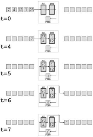
If the length of the input sequence is greater than twice the number of sorting units, an ex-ternal memory is needed. In Fig. 7 an example of sorting a three-key input sequence with one sorting unit is reported; a one-element FIFO is used.
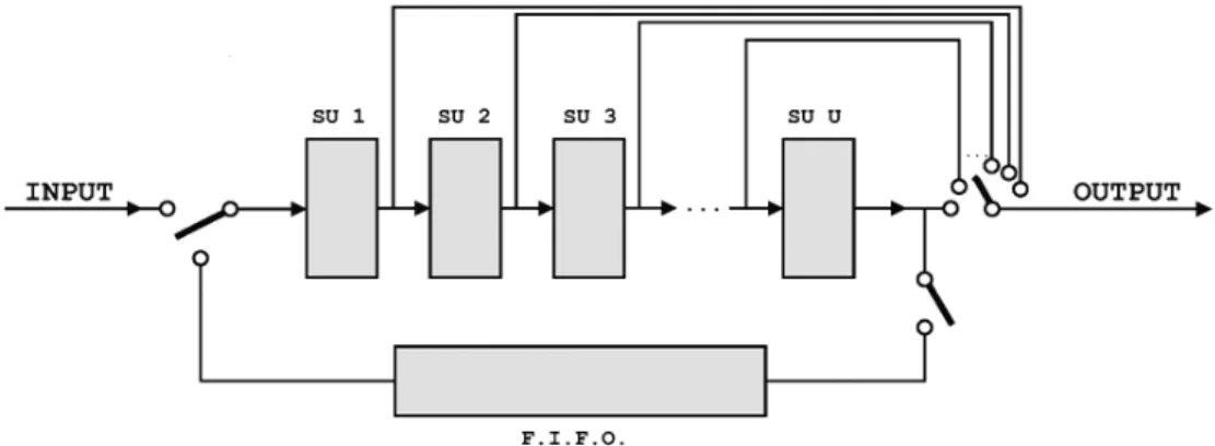
The block diagram of a sorting device built with SUs and FIFO is shown in Fig. 6. A sorting ex-ample is reported in Fig. 8, where two SUs are used together with an external FIFO to order a sequence of five keys.
The speed limits of this architecture depend mostly on the speed of the comparator inside the sorting unit and on the length of the FIFO. Generally speaking, the clock speed depends on the layout of the VLSI, on the technology used, on the number of metal layers and on the cho-sen approach for the design, namely standard cells or full custom; this topic will be further considered later on.
Fig. 7. Sorting example of three keys with 1 SU and 1-element FIFO. The delimiter symbol # represents
a number greater than all the keys in the sequence.
Regarding the computational complexity of the algorithm in the case N > U +1, we have to
consider two cases separately, namely when N
Fig. 8. Sorting example of five of the keys with 2 SU.
is less or equal to 2U and when N is greater than 2U. In the first case, in fact, there is no need for a FIFO external storage, since all the data can be contained in the U sorting units, and the switch depicted in Fig. 8 is connected to the A position, while in the latter case when all the data enter the device, the switch is connected to the B position to allow the re-circulation of the data into the sorting units to complete the sort-ing. Of course, when the switch is in position B, no new data can enter the device.
The complexity of these two cases is described in the following Proposition.
Fig. 9. Sorting time(in terms of number of cycles)vs.
input size for the currently described algorithm. Different curves have been obtained by varying the
Proposition 3. The complexity of the device, expressed in terms of number of clock cycles, is the following
datasize FIFOsize complexity
(S+1)<N2U 0 2U+N+2Pr
N>2U N;2U N(Pi+1)+2Pr
The results described in Propositions 2–3 are reported in Fig. 9, where a family of curves is shown, from the upper part of the panel to the lower, for 1, 3, 7, 15, 31, 63, 127 and 255 sort-ing units. On the ordinate, the number of clock cycles is represented.
2.5. Comparison with Other Algorithms
An obvious way of sorting N integers is to store the number in a computer memory and use a known sorting algorithm. Of course this ap-proach is not convenient, in terms of circuit area and running time trade-off, with respect to VLSI implementations. It is interesting, however, to compare the running time of some known serial sorting algorithms with the time required by the sorting architecture proposed in this paper. One problem in such a comparison is the de-finition of the practical aspects of the software implementation, namely the efficiency of the compiler or the characteristics of the computer hardware. In order to overcome these difficul-ties, we have chosen Knuth’s MIX assembly language, which refers to a very simple archi-tecture 14]. The proposed VLSI algorithm,
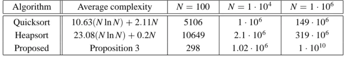
with the number of sorting units fixed to 99, has been compared with a couple of O(N ln N)
algo-rithms, namely the Quicksort and Heapsort, for different values of input size. Table 1 compares, in terms of clock cycles, the complexity in dif-ferent cases. Table 1 shows that the proposed VLSI algorithm, with 99 sorting units, has bet-ter or similar time complexity than O(N ln N)
serial algorithms with up to 110
4input
num-bers. In general, the number of sorting units
required by the proposed algorithm in order to get a lower sorting time than O(N ln N)
algo-rithms, is approximately given by
U
N
k ln N : (4)
The approximation given by this result is asymp-totically better; that is, it is better as N increases. The value of “k" in this equation is the complex-ity coefficient of the software algorithm. For example, from Table 1, it is 23 for the Heapsort.
3. VHDL Design of the Sorting Algorithm
The VLSI design has been performed using VHDL descriptive language; with VHDL, it is quite easy to verify and improve design deci-sions and to test if the initial specifications are met. A behavioural study represents the higher abstract level in the description of an electronic device. In this Section, the behavioural aspects of the device, in response to the external stimuli, are given. A commercial VHDL compiler has been used in this phase.
3.1. Design of a Sorting Device
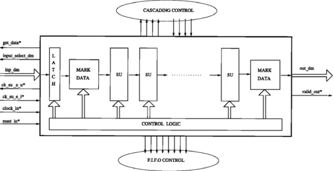
A sorting device performs the sorting of the in-put data; its block diagram is depicted in Fig. 10. The data enters from the input inp dm and exits – sorted according to the key field – to the output out dm. The signals depicted on the left side of Fig. 10 manage the data source and the data switch, the signals on the right side deal with the output devices, the signals on the bottom control the external memory and those on the top deal with the cascading mechanism. Internally, a control logic manages the function of the other internal and external circuits. The latch has a delay function and the mark data blocks are used to furnish a reference for the re-circulation function.
Algorithm Average complexity N=100 N=110
4
N=110
6 Quicksort 10:63(N ln N)+2:11N 5106 110
6
14910
6 Heapsort 23:08(N ln N)+0:2N 10649 2:110
6
31910
6
Proposed Proposition 3 298 1:0210
6
110
10
Fig. 10. Diagram of a sorting device.
3.1.1. Sorting Unit
The fundamental component of the sorting block is the Sorting Unit (SU). The signals ing, usc,
clk, res n3 are the input, the output, the clock and the reset respectively. The signals Sle and Fle are respectively the value of the last S – or Sorted bit, as described previously – and of the last F bit – whose function is to separate blocks of data in the stream – entered in the sorting unit. Moreover, Slen and Flen are the penul-timate values of the corresponding bits entered in the SU. The definition of a sorting unit in VHDL is described as:
entity su is
port (ing:in e_bus usc:out e_bus clk:in bit res_n:in bit
Sle,Fle,Slen,Flen:out bit )
end su
The e bus is used for connecting the SU and its format is described in Fig. 5. In addition to the sorting function and to the separation between data blocks, in the design of the SUs, a power saving function has also been considered. As-sume, in fact, that we have a block of N words to be sorted and that the sorting block contains a cascade of U sorting units with U >(N;1).
After the N words have passed (N ; 1) SUs,
the comparator of the remaining SUs, from N to U, can be turned off, because all the needed comparisons have been already performed.
3.1.2. Behavioural Description of the Sorting Unit
The introduction of the F and S bits, as described in sec. 2.4.1, and some considerations on power saving allow us to provide the complete func-tional description of the sorting units reported as pseudocode in Fig. 11. In order to reduce the dimension of the pseudocode, instead of con-sidering the couple of physical registers D0, K0
and D1, K1 and of the related bit F0, S0 and
F1, S1, we consider the last entered data, called
Dle, Kle and the penultimate data that entered the SU, called Dlen, Klen.
The meaning of the variables used in Fig. 11 is the following: Fu and Su are the values that the F and S bits assume according to the values of the Sle, Fle, Slen and Flen registers. These registers are updated from the data at the input of the unit on the rising front of the clock. The PS bit shows how the content of the power sav-ing register is besav-ing modified; value “1” means that the register must be set, value “0” means
3
Reset
for each clock cycle do {
// Fle Sle Flen Slen Fu Su are single bits COND = Fle Sle Flen Slen
// COND is composed by four bits: // F and S of the last entry
// and the internal state Flen e Slen case COND 0000 : Fu=0 Su=0 perform_action(NC) 0001 : Fu=0 Su=0 perform_action(NC) Slen=0 0010 : Fu=1 Su=0
PS=1 // Power Saving perform_action(PS) Flen=0
0011 :
Fu=1 Su=1
PS=1 // Power Saving perform_action(PS) Flen=0
0100 :
Fu=0 Su=E
PS=0 // Power Saving inactive perform_action(NC) 0101 : Fu=0 Su=1 perform_action(NC) 0110 : Fu=1 Su=0 perform_action(NC) Flen=0 Slen=1 0111 : Fu=1 Su=1 perform_action(NC) Flen=0
1000 or 1001 or 1100 or 1101 : Fu=0 Su=0
PS=0 // Power Saving inactive perform_action(ALlen)
1010 or 1110 : Fu=1 Su=0
PS=0 // Power Saving inactive perform_action(ALlen)
1011 or 1111 : Fu=1 Su=1
PS=0 // Power Saving inactive perform_action(ALlen)
Fig. 11. VHDL pseudocode of the SU functional
algorithm. Each sorting unit has another two bits, called SLen and Flen, which record the values of the last S and
F entered in the sorting unit.
that the register must be reset. The variation of the content of this register shall be effective in correspondance to the rising front of the clock. When the PS register is set, the action to per-form is always ALlen, i.e. the data before the next exits and a new data enters.
The action NC(i.e. Normal Comparation)lets
the field that contains the smaller key out from the sorting unit. It is important to note that the variable Su can assume the value E that indi-cates an error condition: this case cannot occur during the normal functioning of the integrated sorting circuit. If this happens, it means that the sorting block is damaged, or that it is used in a wrong manner, or that there are short circuits at its inputs, or that the maximum functioning speed is overreached. In Fig. 11, there are no references to the values of the key used for the sorting, and this allows us to perform the key comparation, the Su and Fu calculation and the evaluation of the next action.
3.2. Scaling the Sorting Operation
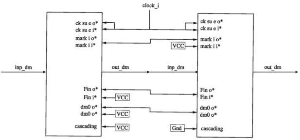
The functional description reported above has been used for the architectural design of the sorting block and for performing tests with dif-ferent input sequences. Here we describe how sorting blocks can be connected in cascade to extend the capability of the sorting device. The block diagram depicted in Fig. 12 represents the cascading operation of the sorting VLSI de-vices. As it is shown in the figure, four lines are sufficient for cascading: input and output lines, clock and cascading lines. The input and output lines are connected between couples of sorting blocks, and the cascading input deter-mines whether a sorting unit is the slave or the master of the cascade. More precisely, if cas-cading is set to zero level, then the sorting block is the master. Hence, all but the last of the sort-ing blocks of the chain set their cascadsort-ing input to a high level, and the last sorting block fur-nishes the clock to the others according to its fan-out.
Fig. 12. Cascade of two sorting blocks.
bit sorted flow. In this way, the data upsizing can be increased in steps of 16 bits. The key field, which is the basis of the sorting process, is left unchanged to the original 16 bits. Unfortu-nately, the key upsizing is not so easy as the data upsizing, because it would require either some additional external logic or a chip redesign.
Fig. 13. Data upsizing.
4. VLSI Synthesis
4.1. Structural Synthesis
In Section 3 we highlighted the VHDL design of the sorting block using a behavioural model. The next step, dealt with in the current Sec-tion, is to convert the behavioural design to a structural description. Generally speaking, this task can be accomplished in two ways, named manual or automatical. In the former (custom
approach), a structural description can be
ob-tained using a layout editor like MAGIC 19];
in this case the work is done manually by the designer who, among other things, must have a high degree of knowledge about the VLSI tech-nology since transistors and wirings are directly designed on silicon. Very high degrees of effi-ciency can be obtained; this solution, however, is possible only for simple chips. The other pos-sibility is to use automatic tools, that can convert the behavioural description into a structural one using a set of standard cells. The latter solution was adopted in this work. The system used for the structural synthesis was ALLIANCE 3].
The behavioural description of the sorting block is automatically converted(using the Alliance
tool logic) to a structural description. The
blocks have been simulated first with differ-ent input patterns using the tool asimut, and
Fig. 14. SU structural design.
K&D CMP SS COND
number of microcells 8 16 17 15
number of gates 257 98 48 25
number of inverters 50 26 11 8
area occupationgrids] 1246 417 231 89
longest pathgates] 3 9 5 3
Table 2. Main characteristics of the structural design.
then, the code of each block was optimized with logic-o for both speed and area occupation. Moreover, to avoid fan-out problems, some buffers are inserted in critical points of the cir-cuit with the Alliance tool netoptim. In Fig. 14 the structural design of the sorting unit is de-picted. It is composed of four blocks:
K&D: containing registers for keys and data
and an output multiplexer;
CMP: performs the keys comparison; SS: composed by registers for storing the
state of the sorting unit (in particular Sle,
Fle, Slen, Flen);
COND: combinatorial circuits.
The main characteristics of the structural design are reported in Table 2.
Finally, structural descriptions of the four blocks were connected with the tool genlib.
In conclusion, to comply with the design, the sorting unit requires 428 gates and an area of 1983 grids.
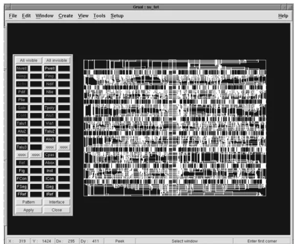
4.2. Silicon Synthesis
This section deals with the generation of the Caltech Intermediate File (CIF). The goal is
to deliver the sorting unit as a new macrocell,
which could be used in the actual chip design or as a subsystem of other designs. In the first step, positioning and interconnection of the cells se-lected from the standard library are performed. The silicon synthesis phase is then verified in several ways.
The final structure can be viewed with the Alliance tool graal, which is a layout editor. The entire sorting unit is reported in Fig. 15.
5. Final Remarks and Conclusions
In this paper the design of a sorting block based on the connection of a number of elementary Sorting Units(SU)working in pipeline has been
described. Its main advantage is its simplic-ity, which makes it highly suitable for a VLSI implementation. Moreover, the overall sorting system is scalable, and this is fundamental from a practical point of view. Other faster algo-rithms do exist, but at the expense of versatility and simplicity.
It is worth emphasizing that sorting is performed on a stream of data according to the value of a key which accompanies the data; in the cur-rent design, the key is a 16 bit unsigned num-ber. Other numerical representations of the key field, typically 2’s complements, would require a re-design of the CMP block only. On the other hand, the numerical representation of the data field doesn’t care about this, because the data field is only passed on.
A detailed analysis of the computational com-plexity has been briefly summarized and a VHDL description has been reported. Recall that to sort N input words we need to connect
(N ;1)Sorting Units(SU), and note that one
SU can be implemented usingα1+α2k grids,
where k is the total number of bits of the key and data registers andα1,α2 are structural
synthe-sis constants(by the way, from Table 2, one SU
requires about 2000 grids for 16 bit data and 16 bit keys). Thus, we can say that the area needed
to sort N input words is O(kN). Since the time
is O(N), we have that A T =O(kN 2
), which
should be compared with the theoretical bound
Ω(N ln N). In this latter sense, the design is
reasonable in terms of area and time trade-off. For the sake of comparison, in Table 3, where p = ln N, we report the AT and I=O orders of
Method AT I=O
Odd-even O(kN
2
) O(k+p)
Proposed design O(kN
2
) O(k) Table 3. AT and I=O trade-offs for different designs.
complexity of the well-known odd-even trans-position design, as reported in 20], and the
de-sign described in this paper.
Many improvements are currently being stud-ied. For example, the possibility of modifying ascending or descending sorting directions can be very easily taken into account by adding an inverter to the logic output of the comparator. Another useful improvement that can be con-sidered in successive versions of the design is the inclusion of a path for controlling possi-ble breakdowns in the internal SUs; this can be easily obtained using a shift register.
It is worth noting, finally, that the possibility of realizing sorting devices directly on a FPGA can be considered, as, using Alliance, this becomes particularly simple.
References
1] B. AHN ANDJ. M. MURRAY, A pipeline, expandible
sorting engine implemented in CMOS technology, in IEEE Int. Symposium on Circuits and Systems, ISCAS89, 1989, pp. 134–137.
2] G. ALEXIOU ANDD. STILIADIS, Design and
imple-mentation of a highperformance, modular sorting engine, in IEEE European Design and Test
Confe-rence, 1994, pp. 2–8.
3] Alliance, http://www-asim.lip6.fr/
alliance.
4] K. E. BATCHER, Sorting Networks and their
Appli-cations, in Proc. AFIPS Spring Joint Comput. Conf., Vol. 32, 1968.
5] A. BELLETTINI, A. FERRARI, R. GUERRIERI,ANDG.
BACCARANI, A digital parallel VLSI architecture for fuzzy database mining, in IEEE World Congress
on Computational Intelligence, 1994.
6] G. M. BLAIR, Low Cost Sorting Circuit for VLSI, IEEE Trans. on Circuits and Systems, 1996. 7] V. BRAJOVIC AND T. KANADE, A VLSI sorting
image sensor: global massively parallel intensity-to-time processing for low-latency adaptive vision,
IEEE Trans. on robotics and automation, 1999, pp.
8] C. CHAKRABARTI, Sorting Network Based
Archi-tectures for Median Filters, IEEE Trans. on Circuits
and Systems-II, 40, 1993.
9] T. C. CHAN, K. P. ESWAREN, V. Y. LUM, AND C.
TUNG, Simplified Odd-even Sort Using Multiple Shift-Register Loops, Int. J. Comput. Inform. Sci., 7, 1978.
10] T. CORMEN, C. LEISERSON,ANDL. RIVEST,
Intro-duction to Algorithms, The MIT Press, 1990.
11] S. B. GULIN, A expansibile current-mode sorting
integrated circuit for pattern recognition, in Int.
Joint Conference on Neural Network, vol. 5, 1999,
pp. 3123–3127.
12] J. JA’JA ANDR. M. OWENS, VLSI Sorting with
Re-duced Hardware, IEEE trans. on Computers, vol. C-33, 1984.
13] M. KARAMAN, L. ONURAL,ANDA. ATALAR, A
gen-eral purpose VLSI median filter and its application for image processing, in Melecon 89, 1989, pp. 366–369.
14] D. E. KNUTH, The Art of Computer Programming, Sorting and Searching, Addison Wesley, 1975. 15] M. KUMAR AND D. D. HIRSHBERG, An Efficient
Implementation of Batcher’s Odd-even Merge Al-gorithm and its Application in Parallel Sorting Schemes, IEEE Trans. on Computers, vol. C-32, 1983.
16] J.-D. LEE ANDK. E. BATCHER, Minimizing
Com-munication in the Bitonic Sort, IEEE Transaction
on Parallel and Distributed Systems, 2000.
17] C.-S. LIN ANDB.-D. LIU, Design of pipelined and
expandable sorting architecture with simple con-trol scheme, in IEEE International Symposium on
Circuits and Systems ISCAS 2002, 2002.
18] E. E. LINDERSTROM ANDJ. S. VITTER, The design
and analysis of bucket sort for bubble memory secondary storage, IEEE Trans. on Computers, vol. C-32, 1985, pp. 218–233.
19] Magic, http://bwrc.eecs.berkley.edu/
Classes/IcBook/magic/index.html
20] G. M. MEGSON, Sorting without exchanges on a
bit-serial systolic array, IEE Proceedings, 137, 1990, pp. 345–352.
21] G. MIRANKER, L. TANG,ANDC. K. WONG, A
zero-time VLSI sorter, IBM J. Res. Develop., 27, 1983, pp. 140–148.
22] D. NASSIMI ANDS. SAHNI, Bitonic Sort on a
Mesh-Connected Parallel Computer, IEEE Trans. on
Com-puters, vol. C-28, 1979.
23] S. OLARIU, M. C. PINOTTI,ANDS. Q. ZHENG, An
Optimal Hardware-Algorithm for Sorting Using a Fixed-Size Parallel Sorting Device, IEEE
Transac-tion on Computers, 2000.
24] I. PITAS ANDA. N. VENETSANOPULOS, Non Linear
Digital Filters, Kluwer Academic Publishers, 1990.
25] D. S. K. POK, C. I. H. CHEN, J. J. SCHAMUS, C.
T. MONTGOMERY,ANDJ. B. Y. TSUI, Chip design for monobit receiver, IEEE Trans. on Microwave
Theory and Techniques, 45, 1997, pp. 2283–2295. 26] D. C. STEPHENS, J. C. R. BENNET,ANDH. YHANG,
Implementing scheduling algorithms in high speed networks, IEEE Journal on Selected Areas in
Com-munications, 1999.
27] C. D. THOMPSON, The VLSI Complexity of Sorting, IEEE Trans. on Computers, vol. C-32, 1983. 28] J. D. ULLMAN, Computational Aspect of VLSI,
Computer Science Press, 1984.
29] H. YASURA, N. TAGAKI,ANDS. YAJIMA, The
par-allel Enumeration Sorting Scheme for VLSI, IEEE
Trans. on Computers, vol. C-31, 1982, pp. 1192–
1201.
Received: February, 2003 Revised: March, 2004 Accepted: March, 2004
Contact address:
Enzo Mumolo DEEI, University of Trieste Via Valerio 10 34127 Trieste, Italy Phone:+39.040.558.3861
Fax:+39.040.558.3460
e-mail:[email protected]
Massimiliano Nolich e-mail:[email protected]
ENZOMUMOLOreceived a Dr Eng degree(magna cum laude)in
elec-trical engineering from the University of Trieste, Italy, in 1982 and then joined the Central Laboratory of Alcatel Italia, FACE division, formerly FACE Res. Center, in Pomezia, Rome, Italy. In 1985 he was with ITT DCD-West in S. Diego, CA. In 1987 he became responsible for research activities within the Speech Processing Dept. of Alcatel Italia, FACE Division. From 1990 to 1991 he was with Sincrotrone Trieste, Italy, as head of the Electronics Group. In 1991 he joined the Computer Science Dept. at DEEI, University of Trieste, as research engineer and assis-tant professor. His current research interests include nonlinear systems, adaptive filtering, operating systems and speech processing. Member of IEEE, ACM and AEI, he has published more than 100 papers in professional journals and international conferences proceedings and he holds two United States Patents.
GABRIELECAPELLOreceived a Dr Eng degree in electronic engineering in 1997. He spent two years as visiting scientist in International Centre for Theoretical Physics(I.C.T.P.)Miramare, TS, Italy working on two
main projects: fast-moving imaging system, sort chip implementation. For four years he worked as digital electronic engineer in Telit(Sgonico,
TS, Italy)working on the design of several cellular phone terminals.
Now he is a digital electronics engineer in Neonseven(Sgonico, TS,
Italy), working on reference designs for cellular phones.
MASSIMILIANONOLICHreceived a Dr Eng degree in electronic engi-neering in 1999(magna cum laude)and Ph.D. degree in 2003 from