CMOS camera and a computer. The circuit enables the user to take pictures with the camera
and transfer it to computer. The circuit uses an AVR microprocessor (ATMEGA16) as the
central processing unit. The camera is ov6620 produced by Omnivision. It is an IR camera
and has both digital and analogue output.
Keywords: Digital Camera, AVR, I2C, RS-232
* Lecturer, Department of Computer Engineering and Information Technology, Payame Noor
University, Tehran, Iran
** Department of Artificial Intelligence, Science and Research Branch, Islamic Azad
1.
INTRODUCTION
This research aims designing and developing an intermediary circuit to connect a camera
-CMOS-C3088- to computer using an AVR microprocessor. The design is based on a project
conducted by (Oiza, 2004) There are two data flows: first the commands which are
transmitted from computer to the camera and second, the picture taken by the camera from
the camera to the computer.
The interface between computer and AVR uses serial port RS232, while the interface
between camera and AVR uses I2C protocol for accessing camera’s registers and a 8-bit port
for reading the picture. These 8 bits are transferred using 8 pins of IDC. The camera can also
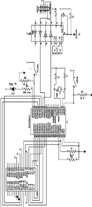
be connected to a TV using analogue output. The schematic is shown in figure 1.
Figure 1: Interconnection Schematic
2.
HARDWARE
The C3088 camera has a digital output and benefits from a visual CMOS sensor OV6220
from OmniVision. The digital port transmits the data as 8 or 16 bits data flow. All the
functionality of the camera is configurable by changing the camera registers with I2C
interface.
The output of the camera can be shown as different RGB or UYV channels. In this project we
use the Y channel with 8 bits to represent the intensity of each pixel. The U and V channels
are not used. The information is send sequentially and synchronization is done by HREF,
YSINK and PCLK signals. YSINK signal shows the start of new frame, HREF signal is the
time when data is valid and PCLK is the clock signal. This is enough for reading the picture
from camera by microcontroller without any extra hardware. These signals are shown in
The ID address of camera for writing is 0xc0 and 0xc1 for reading. The pin configuration of
camera is as follows:
• Y0 to Y7: digital bus of Y output
• UV0 to UV7: output bus of UV
• PWDN: Power down mode and RST Reset
• SDA: serial I2C input
• SCL: input I2C serial clock
Hardware configuration is discussed here. The VCC voltage is 5v.
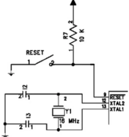
2.1
RESET and CLK
The reset part is pulled up with a 10K resistor and a switch to ground on reset. A 16 MHz
crystal with two 2pf capacitors are used as external oscillator. The crystal is connected on
Figure 3: External Crystal Circuit
2.2
LED and SWITCH
And LED is used on PD7 pin for debugging purposos. Also a pulled up switch is connected
to PD6. This configuration is showed in figure 4.
Figure 4: LED and SWITCH Circuit
2.3
Serial Connection
As the TTL level of microprocessor is not compatible with computer, we should use a
Max232. PD0 (RXD) and PD1 (TXD) should be connected to ports 2 and 3 of RS232. This is
Figure 5: Serial Connection Circuit
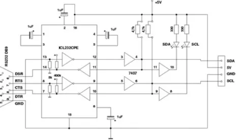
2.4
I
2C and RS-232
Due to wide use of RS-232 in connecting different devices, an interface that is capable of
connecting RS-232 to I2C can give so much flexibility to electronic designers. A sample
circuit is shown in figure 6.
Figure 6: RS-232 Serial Interface Adapter for the I2C Bus
In this project AVR microcontroller works as master and the camera is slave. Camera
registers can be written or read by AVR. At first master puts the address of the devices that
want to read from, on the bus. Then the address of read register is put on the bus. At last, the
slave puts the requested data on the bus.
I2C protocol in this project is written by customizing TWI (two wire interface) which is built
2.5
C3088 camera
The operation voltage of this camera is 5v. This voltage is connected directly to pins 20 and
22 of the camera. Ports 31, 21 and 15 are connected to common ground. As all the reset are
commanded via software, PWDN and RST ports are grounded.
Y0 to Y7 (Y bus of camera) are connected to port A of microcontroller (PA0 to PA7).
PCLK is connected to PD2, HREF is connected to PD3 and VSYNC is connected to PD4. As
UV is not used in this configuration it is not necessary to connect the specified bus to
microcontroller. To use I2C protocol appropriately, SDA and SCL pins of camera should be
connected to PC1 and PC0 pins of microcontroller. These two pins are connected to TWI
hardware of microcontroller which run I2C protocol. VTO pin is analogue video output which
Figure 7: C3088 Camera Circuit Schematic
3.
SOFTWARE
All the codes in this project are in C language. Some of the parts are described here.
3.1
Serial Communication
The communication using serial port would implement the communication between computer
and microprocessor. We can proof that the system is working by communicating via this
channel. A serial communication program like HyperTerminal can be used on computer to
The appropriate code is fetched from ATMEL USART library for GCC compiler. The code
has been customized for this project. The bytes would be received by an interrupt and saved
in a buffered. This is the only interrupt used by the system. There is no buffer to send the
bytes.
3.2
I
2C Communication
One of the most important parts of control systems is data communication. Researchers are
working to develop a reliable, fast and secure protocols for this aim. The I2C protocol has
been invented by Philips in 1980’s to communicate between TVs and processors. It has been
widely used by electronic manufacturers because of its simplicity and speed.
I2C stands for Inter IC that represents its aim, providing a communication link between
integrated circuits. Nowadays, this protocol is used generally in electronic industry beyond
audio/video instruments. There are more than 1000 ICs which implement and support this
protocol.
3.2.1 I2C benefits
I2C brings simplicity and speed for designing integrated circuits. Operation block diagram is
fully compatible with real ICs and designer can gain the final schematic rapidly. There is no
need to design an interface because it is implemented on-chip and impedance matching
calculations would be omitted. It is controllable via hardware or software. We can add or
remove appropriate ICs. Software design time would be reduced so much because of
presence of prepared libraries.
Also due to the technology of manufacturing I2C compatible devices, they can gain the
benefits mentioned below:
1. Low current consumption
2. Acceptable noise tolerance
3. Wide range of working voltage
4. Wide range of temperature tolerance
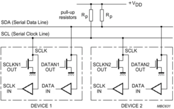
3.2.2 I2C bus hardware
There are two main data lines:
- Serial Data Line (SDA)
- Serial Clock Line (SCL)
As these two lines transmit data in both ways, we can have more than one master or each
Figure 8: SDA and SCL Data Lines
Though the technique of open-collector and using pull-up resistors would give the ability of
wired-and, but in long data lines which make capacitance field it might make RC properties.
To solve this problem, current sources could be used instead of resistors.
4.
DATA COMMUNICATION FORMAT
Each byte of data on SDA is 8 bytes long and there is no restriction about number of sent
bytes for each transmitter on SDA. It is important not to change SDA level while clock is
high except two modes which show start and stop.
START bit: changing logical level of SDA from high to low while clock is high
STOP bit: changing logical level of SDA from low to high while clock is high
Bit transfer on the I2C bus and START and STOP conditions are shown in figures9 and 10.
Figure 9: Bit Transfer on the I2C Bus
Figure 10: START and STOP Conditions
means that the byte has not been received, otherwise if SDA goes down it means that the byte
has been received properly.
4.1
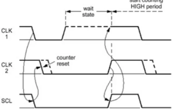
Synchronizing clock pulse
Clock pulses are made by Masters. Each master puts its clock pulse on SCL. As the
wired-AND bus is used, the clock pulses are wired-AND and there would be common clock pulse.Clock
synchronization is shown in figure 11.
Figure 11: Clock Synchronization during the Arbitration Procedure
4.2
Addressing:
To address each device in this protocol we need an addressing method. For each device some
of the bits are addressed on-chip and others are address by hardware. At first 7-bit address
was used, but now by developing the bus and using more devices an address with 10 bits is
used.
4.3
BMP
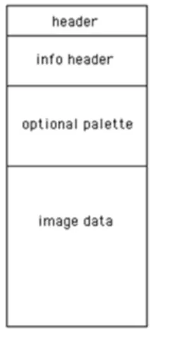
Bitmap image (BMP) is the selected format for transferring the captured image to computer.
This selection is because only the information of each pixel is transmitted after header. This
specification allows us to transfer the image just while capturing it. This properties is so
important as there is no need for extra memory nor any program to render the image in the
computer.
The format of BMP file follows:
- Header: contains file information and is 14 bytes long
- Info Header: contains image information
- Palette: translates each pixel’s information to color
As the basic frequency of PCLK is 17.73 MHz and AVR is not so fast to read each pixel two
solutions would be used:
- Using extra hardware for reading and saving image
- Reducing PCLK frequency by writing in 0x11 register
In this project we use the second solution. The appropriate frequency for reading the image
depends on the method used for reading. If we read the image as horizontal lines, the
minimum frequency 69.25 KHz must be used. This allows us to save the image in the AVR’s
memory as soon as a line is read. Another method is to read a vertical line of image in each
frame. In this method the maximum frequency is 260 KHz. But we need to read a lot of
frames as vertical lines to complete an image. Nevertheless we use the later method because
in the first method the captured image is so bright.
When we want to transmit the image to computer, headers and palette are transmitted first
and then we read the image from camera. We read the first frame and column and the
transmit it to the computer pixel by pixel.
5.
RESULTS
The image is ready to be seen on computer after interconnecting the hardware and loading the
software. After running HyperTerminal on computer and hitting enter key the message is
shown:
....Control Camera Program....
… Mostafa, Safar and Mohsen Winter 2012 …
By typing Help the menu is shown: ACK HELP MENU-Commands: RESET MIRRORON MIRROROOFF PHOTO TESTBMP
The commands are as follows:
• RESET: reset all registers of camera to their initial value
• MIRRORON: mirrors the picture
• MIRROROFF: turns the mirror property off
• PHOTO: sends a BMP file to the computer which contains the captured photo by
camera. The frequency of PCLK is reduced by microcontroller and one column is read
for each frame. As a result, the image would be captured in 90 seconds and sent to
computer at that time. Because of long time of capturing only static images would be
captured. The resolution is 352x244 pixels. We should save the received information in
the computer terminal and create a bmp file.
• TESTBMP: sending a software created BMP to computer. This photo is created by some
control loops in the microcontroller.
Figure 14: Some of Captured Photos
Some photos of the camera and implemented circuits are shown below.
Figure 15: Photos of Camera and Implementd Circuits
6.
REFERENCES
[1] I. N. Oiza, “Digital Camera Interface,” 2004. Available:
www.robozes.com/inaki/dproject/report.pdf.
[2] A. K. Ray and K. M. Bhurchandi, Advanced Microprocessors and Pripherals, 2nd ed.
Tata McGraw-Hill Educaiton, 2009, p. 717.