Features
Compliant with IEEE 802.3u standard
Link distance at 100Mbps: up to 100m per IEEE802.3 EEPROM with serial ID functionality
Detailed product information in EEPROM
Industry standard small form pluggable (SFP) package Compact RJ-45 connector assembly
Fully metallic enclosure for low EMI +3.3V single power supply
Application
SFP over 10/100Mbps copper Ethernet Distributed multi-processing
High speed I/O for file server or high-end workstation Switch/Router to Switch/Router Link
Description
APAC SFP-T1 10/100BASE-T copper SFP transceiver is high performance, cost effective module compliant with the 100Mbps Fast Ethernet and 100BASE-F standards as specified in IEEE 802.3, which supporting 100Mbps data- rate up to 100 meters reach over UTP cable. The SFP-T1 supports 100 Mbps full duplex data-links with 3-level Pulse Amplitude Modulation (PAM) signals. The SFP-T1 provides standard serial ID information compliant with SFP MSA, which can be accessed with address of A0h via the 2-wire serial EEPROM protocol.
Ordering Information
PART NUMBER INTERFACE Speed Mode VOLTAGE TEMPERATURE
SFP-T1 LVPECL Auto-negotiation 10/100Mbps 3.3V 0°C to 70 °C SFP-T1A LVPECL Auto-negotiation on and
100 Mbps full duplex only 3.3V 0°C to 70 °C SFP-T1B LVPECL Auto-negotiation off and
Absolute Maximum Ratings
PARAMETER SYMBOL MIN MAX UNITS NOTE
Storage Temperature Ts -10 80 °C
Supply Voltage Vcc 3.0 3.63 V
Recommended Operating Conditions
PARAMETER SYMBOL MIN MAX UNITS NOTE
Operating Temperature T 0 70 °C
Supply Voltage Vcc 3 3.45 V Typ. 3.3V
Power Consumption P 560 mW
Supply Current I 170 mA
Surge Current Isurge 30 mA Hot Plug
Electrical Characteristics
Vcc = 3 V to 3.6 V, T = 0°C to 70°C
PARAMETER SYMBOL MIN TYP. MAX UNITS NOTE
Transmitter
Data Input differential Voltage VD,TX 0.25 --- 1.20 V 1
Differential Input Impedance ZTX 80 100 120 Ohm
Transmitter Disable Input-High VDish 0.6* Vcc --- --- V
Transmitter Disable Input-Low VDISL --- --- 0.4* Vcc V Receiver
Data Output Differential Voltage VD,RX 0.35 --- 0.8 V 1
Differential Output Impedance ZRX 80 100 120 Ohm
Data Output Rise/Fall Time Tr,,RX /Tf,,RX --- 2 --- nS 2
LOS Output VSDHL 0 --- Vcc+0.3 V
Note:
1) Internally AC coupled and terminated to 100 Ohm differential load. 2) 20% ~80% value
Power Coupling
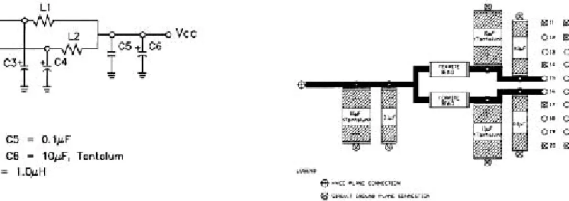
A suggested layout for power and ground connections is given in Figure 1 below. Connections are made via separate voltage and ground planes. The mounting posts are at case ground and should not be connected to circuit ground. The ferrite bead should provide a real impedance of 50 to 100 ohms at 100 to 1000 MHz. Bypass capacitors should be placed as close to the 20 pin connector as possible.
Figure 1: Suggested Power Coupling
Connection Diagram
Pin-OutPIN 1
PIN 10
PIN 20
PIN 11
Pin Signal Name Function NOTES
1 VeeT Transmitter Ground VeeT and VeeR are connected in SFP.
2 TX_FAULT Transmitter Fault Indication Not Implemented. Floating.
3 TX_DISABLE Transmitter Disable Not Implemented. Floating.
4 MOD DEF (2) Module Definition 2 Data Line for Serial ID.
5 MOD DEF (1) Module Definition 1 Clock Line for Serial ID.
6 MOD DEF (0) Module Definition 0 Tied to Vee in SFP-T1.
7 RATE SELECT Not Implemented Not implemented.
8 LOS Loss of Signal Loss of Signal
9 VeeR Receiver Ground VeeT and VeeR are connected in SFP.
10 VeeR Receiver Ground VeeT and VeeR are connected in SFP.
11 VeeR Receiver Ground VeeT and VeeR are connected in SFP.
12 RD- Inverted Received Data out AC coupled 100 ohm differential high speed data
lines.
13 RD+ Non-Inverted Received Data out AC coupled 100 ohm differential high speed data
lines.
14 VeeR Receiver Ground VeeT and VeeR are connected in SFP.
15 VccR Receiver Power VccR and VccT are connected in SFP.
16 VccT Transmitter Power VccR and VccT are connected in SFP.
17 VeeT Transmitter Ground VeeT and VeeR are connected in SFP.
18 TD+ Non-inverted Data In AC coupled 100 ohm differential high speed data
lines.
19 TD- Inverted Data In AC coupled 100ohm differential high speed data
lines
3. Mod-Def 0,1, 2. These are the module definition pins. They should be pulled up with an 4.7-10 K resistor on the host board to a supply less than VCCT + 0.3 V or VCCR + 0.3 V.
4. RD-/+: These are the differential receiver outputs. They are ac coupled 100 Ohm differential lines which should be terminated with 100 ohm differential. The ac coupling is done inside the module and is thus not required on the host board. The voltage swing levels are compatible with LVPECL voltage swings.
5. VCCR and VCCT are the receiver and transmitter power supplies. They are defined as 3.3 V ± 5% at the SFP connector pin. 6. TD-/+: These are the differential transmitter inputs. They are ac coupled differential lines with 100 Ohm differential termination inside the module. The ac coupling is done inside the module and is thus not required on the host board. The inputs levels are compatible with LVPECL voltage swings.
Drawing Dimensions
Unit : inch
Mating of SFP Transceiver to SFP Host Board Connector
The pads on the PCB of the SFP transceiver shall be designed for a sequenced mating as follows: First mate: Ground contacts. Second mate: Power contacts. Third mate: Signal contacts The SFP MSA specification for a typical contact pad plating for the PCB is 0.38 micrometers minimum hard gold over 1.27 micrometers minimum thick nickel. To ensure the long term reliability performance after a minimum of 50 insertion removal cycles, the contact plating of the transceiver is 0.762 micron (30 micro-inches) over 3.81 micron (150 micro-inches) of Ni on Cu contact pads.
RJ45 Connector