© Science and Education Publishing DOI:10.12691/joe-4-1-3
A Systematic Study of the Optical Properties of Co-, and
Ni- Doped Colloidal Cadmium Sulphide Nanoparticles
P. Bhambhani*, P. A. Alvi
Department of Physics, Banasthali University, Banasthali-304022, India *Corresponding author: [email protected]
Abstract
Present research paper deals with the synthesis and characterization of CdS:Co and CdS:Ni nanoparticles. CdS:Co and CdS:Ni nanoparticles are synthesized with the different concentration of Co and Ni with the use of polyethylene glycol (PEG) as capping agent. Samples are characterized by Scanning Electron Microscopy (SEM), Ultraviolet-Visible (UV-VIS) and Photoluminescence (PL) spectroscopy. The size of synthesized nanoparticles is obtained ~50 nm approximately by SEM images. The effect of doping concentration on optical properties of CdS nanoparticles is studied by UV-VIS and PL spectroscopy. Band gap of Cd1-xCoxS and Cd1-xNixSnanomaterials decreases with doping concentration. The results demonstrate that the doping concentration play an important role in optical features of nanomaterials. On behalf of the outcomes, it can be reported that the nanoparticles can be utilized as a photodetectors operating in visible region of increasing wavelengths.
Keywords
: CdS: Co, CdS: Ni nanoparticles, nanomaterials and PEGCite This Article:
P. Bhambhani, and P. A. Alvi, “A Systematic Study of the Optical Properties of Co-, and Ni- Doped Colloidal Cadmium Sulphide Nanoparticles.” Journal of Optoelectronics Engineering, vol. 4, no. 1 (2016): 11-16. doi: 10.12691/joe-4-1-3.1. Introduction
Preparation of nanomaterials has a great consideration for their distinctive properties which can’t be found from bulk material [1]. The properties of nanomaterials are function of its size unlike bulk materials. The simplest example is semiconducting carbon nanotube whose band gap scales inversely with the tube diameter [2]. In nanotechnology research, allotropes of carbon like Graphene, Fullerene (Buckyball) and Carbon nanotubes are widely used due to their remarkable properties. Electrical and mechanical properties of those allotropes vary with their molecular geometry [3]. The effect of size on properties of nanomaterials is because of two factors: Quantum size effect, i.e. decrease in the particle size and Surface effect, i.e. surface to volume ratio increases[4].
CdS is the most significant II-IV group semiconductor having band gap of 2.42 eV. Because of its outstanding optical properties, it has wide applications in detecting the visible material [5], fabrication of efficient solar cell [6], address decoder [7], electrical driven laser [8], photo detector[9],sensor[10] andphoto resistor[11].
Nanoparticles have drawn great attention of researchers in the various fields of sciences and technologies such as medical science, chemical science, and pharmaceutical science etc. [12,13,14,15]. Many examples of nanoparticle’s synthesis and their applications are discussed as follows:
Marandi
et al. [16] reported combined photochemical–chemical route which enables to grow CdS nanoparticles. CdSO4 and Na2S2O3 were used as reactant in photo-induced
reaction to synthesise CdS nanoparticles and capping
agent was Thioglycerol (C3H8O2S). They reported effect
of pH of the solution on size of CdS nanoparticles. In a recent research, Sajid Husain et al. [17] have synthesized and characterized nano-crystalline undoped and Ni doped ZnO (Ni-ZnO) nano-particles with compositional formula NixZn=O (x=0, 1, 3 and 5 mol %) using sol-gel method.
Most of the work also has been done on Silicon nanoparticles, which are the most promising for the use in CMOS compatible devices. In 2009, V. Donzella et al. [18]
have reported a finite element based model for Si-nc sensitized Er3+ doped waveguide amplifiers (EDWA), longitudinally pumped by a novel pumping scheme using broad-area visible lasers, which accurately describes the effect of the Si-nc to Er3+ coupling ratio on the amplifier performance. Moreover, Ji-Ho Park et al. [19] have studied the biodegradable luminescent porous silicon nanoparticles for in vivo applications. Anoop Gupta et al.
[20] have reported the optical properties of Si nanoparticles. They have demonstrated that the optical properties of Si-nanoparticles depend on their size as well as their surface chemistry. The size of Si- nanoparticles was finely tuned by etching them in a mixture of hydrofluoric acid (HF) and nitric acid (HNO3) for
different times. The resulting Si- nanoparticles exhibit bright luminescence across the visible spectrum. The size-dependent physicochemical and optical properties of silica nanoparticles have been studied by I. A. Rahman et al.
[21].
history of CdS, more recent advances in the chemistry and synthesis of CdS nanostructures, and their application as nanoscale devices in diverse technology areas from electronics to targeted drug delivery has been described in reference [22]. B. S. Rao et al. [23] have studied only structural properties of 2 to 10 % nickel doped cadmium sulfide nanoparticles. They have also studied the influence of increasing concentration of nickel doping on optical properties cadmium sulfide nanoparticles [24].
In the present article, we have synthesized and characterized Co-, and Ni- Doped Colloidal CdS nanoparticles. The effects of variation in concentration of doping element Co and Ni in optical properties of CdS nanoparticles are also reported.
2. Experimental
2.1. Chemical
For the synthesis of CdS:Co and CdS:Ni nanoparticles, Cadmium acetate (Cd(OAc)2·2H2O) (99.9%), Sodium
sulphide (Na2S) (90%), Nickel acetate (Ni(OAc)2·2 H2O),
Cobalt acetate (Co(OAc)2·2H2O) and Poly ethylene
glycol(PEG) (99%), purched from Sigma Aldrich are used without further purification.
2.2. Synthesis Procedure
Nanoparticles of CdS:Co/CdS:Ni were prepared in aqueous medium through chemical coprecipitate methodusing PEG as stabilizing agent. Cadmium acetate, Nickel acetate, cobalt acetate and sodium sulphide are used as Cd+2, Co+2, Ni+2 and S-2 source, respectively. In the typical procedure, 0.5 M Cadmium acetate and Cobalt acetate/ Nickel acetate with different concentration in molar ratio were dissolved in 50 mL deionized water and stirred for 20 minutes at room temperature, during stirring 2 gm PEG was also added to solution. In the second round bottom flask, 0.5 M Sodium sulphide was dissolved in 50 mL deionized water and stirred for 20 minutes. After p[reparing both the solutions, second solution was added to first solution dropwise under constant stirring. The resultant solution was stirred for 3 hours. The solution was cooled at room temperature. The resultant precipitayes were separated from reaction medium by centrifugation and dried in hot air oven at 50°C for 24 hrs.
2.3. Characterization
The absorption spectra were recorded using Perkin Elmer Lambda 750 UV-VIS-NIR spectrometer in the wavelength range of 200-800 nm at room temperature. Photoluminescence (PL) studies were carried out on a Perkin Elmer LS45 fluorescence spectrophotometer using 440 nm excitation wavelength. The morphology and size of the products were examined by a scanning electron microscope (SEM) using Tscan Mira3.
3. Results and Dissucation
3.1. UV-VIS Absorption Spectrum
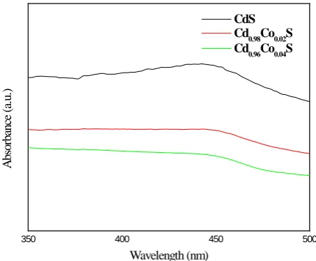
The absorption spectra of Colloidal CdS nannoparticles without and with doping of Ni and Co are measured by
using UV-VIS-NIR photo spectrometer covering wavelength range of 350-500 nm. The UV-VIS absorption specra of CdS:Co and CdS:Ni nanoparticles are measured in the range 350-500 nm at room temperature. The absorption peak for undoped CdS is observed at 445 nm, whereas the peaks for doped Cd1-xCoxS nanoparticles are
observed at 446 nm and 447 nm for x =0.02 and x = 0.04, respectively [Figure 1]. Similarly, these peaks for doped Cd1-xNixS nanoparticles are observed at 448 nm and 453
nm for x =0.02 and x = 0.04, respectively [Figure 2].
Figure 1 and 2 illustrate that as concentration of doping in nanoparticles increases, red shift in absorption peak is observed, which is because of quantum size effect. In absorption spectra of undoped and doped nanomaterials, board and asymmetric peaks are observed, which is due to wide size distribution of obtained nanoparticles.
Figure 1. Absorption spectra for Cd1-xCoxS (x = 0, 0.02 and 0.04)
Figure 2. Absorption spectra for Cd1-xNixS (x = 0, 0.02 and 0.04)
The optical band gap energy of the samples can be calculated from the following equation:
(
)
ng
h k h E
α ν = ν−
where α is absorption coefficient, hν is the incident photon energy, k is unit constant and Eg is band gap energy of the
material. The exponent n depends on the type of transition. for a direct allowed transition n = 1/2 . The band gap energy is calculated by extrapolating the linear portions of
350 400 450 500
A bs or ba nc e ( a. u. ) Wavelength (nm) CdS Cd0.98Co0.02S Cd0.96Co0.04S
350 400 450 500
the (αhν)2 versus hν graph on the hν axis. Calculated energy band gaps for nanoparticles Cd1-xCoxS and Cd 1-xNixS (x = 0, 0.02 and 0.04) are reported in Table 1, which
shows that energy band gap of nanoparticles decrease with increase of doping concentration. Since the reduction in band gap refers to increase in wavelength, hence these nanoparticles can be utilized as a photodetectors, chemical sensors, and optical sensors operating in visible region of increasing wavelengths.
Table 1. Energy band gap of doped nanoparticles Cd1-xCoxS and
Cd1-xNixS
Doping concentration of Co/Ni (x) Band gap (eV)
Cd1-xCoxS Cd1-xNixS
0 2.23 2.23
0.02 2.19 2.13
0.04 2.14 2.02
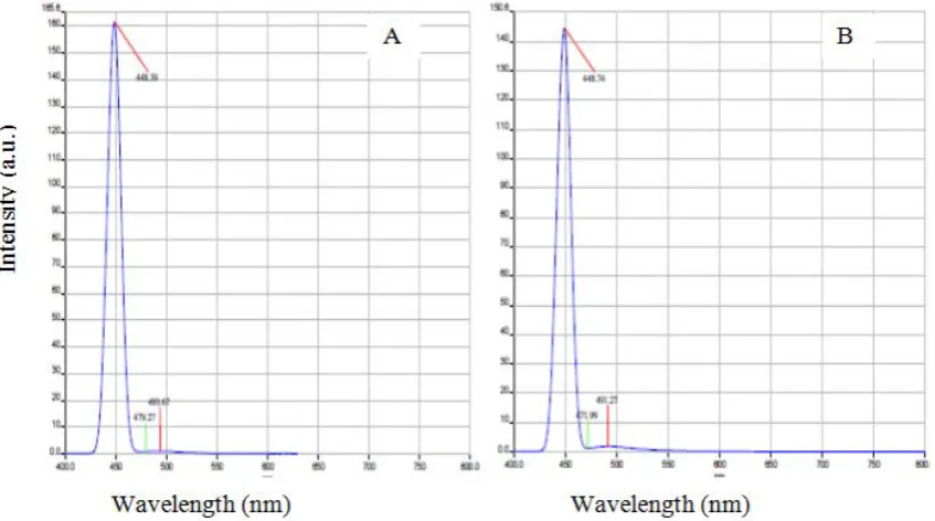
3.2. Photoluminescence Study
The room temperature photoluminescence (PL) spectra of CdS:Co and CdS:Ni nanoparticles at an excitation wavelength 440 nm are presented in Figure 3 and Figure 4, respectively. Photoluminescence peaks positions in CdS:Co and CdS:Ni are listed in Table 2, which shows that as the doping concentration increases in CdS: Co and CdS: Ni nanoparticles, blue emission peak shows slightly red shifting which is corresponding to decrement in energy band gap with doping concentration. From Figure 2 and
Figure 3, it is observed that the fluorescence efficiency of photoluminescence spectra of CdS:Co and CdS:Ni decreases with doping concentration which may be because of increment of transition probability from impurity level to ground state.
Figure 4. Photoluminescence (PL) spectra of Ni-doped CdS with doping concentration 2% (A) and 4% (B)
Table 2. Position of peak and Intensity of PL spectra doped nanoparticles Cd1-xCoxS and Cd1-xNixS
Doping concentration of Co/Ni (x) Position of peak (nm) Intensity (a.u.)
Cd1-xCoxS Cd1-xNixS Cd1-xCoxS Cd1-xNixS
0 448.17 448.17 249.2 249.2
0.02 448.36 448.39 217.5 161
0.04 448.50 448.74 139 144.6
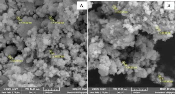
3.3. SEM Analysis
Scanning electron microscope (SEM) is an appropriate method to find the particle size of the nanomaterials. SEM image of synthesized doped and undoped CdS nanoparticles
are presented in Figure 5 and Figure 6. From these SEM image it is noticed that the products are composed of nanoparticles which are uniformly distributed over the entire surface. From SEM images, Particle size of nanoparticles is obtained 50 nm, approximately.
Figure 6. SEM imagea of Ni-doped CdS with doping concentration 2% (A) and 4% (B)
4. Conclusion
In conclusion, Co-doped CdS (Cd1-xCoxS) and
Ni-doped CdS (Cd1-xNixS) nanoparticles were synthesized by
chemical route with different doping concentration x = 0, 2% and 4%. The effects of doping concentration on optical properties of doped CdS nanoparticles were studied by Ultraviolet-Visible (UV-VIS) and Photoluminescence (PL) spectroscopy. It was observed that as doping concentration increases, absorption peak show red shift and band gap of nanoparticles decreases. From Photoluminescence (PL) study, it was investigated that with doping concentration, intensity of blue emission peak decreases, which is correspond to reduction in fluorescence efficiency with doping concentration. These results illustrate that by altering doping concentration, optical features of nanoparticles can be altered. Size of prepared nanoparticles was obtained ~ 50 nm, approximately by SEM images. The outcomes of the observation suggest that the synthesized nanoparticles can be utilized as a photodetectors, or optical sensors operating in visible region of increasing wavelengths.
Acknowledgement
Authors are thankful to DST, Govt. of India for supporting Banasthali University under its CURIE scheme.
References
[1] J.X. Zang, G. L. Zhao and G. R. Han, Preparation of CdS
nanoparticles by hydrothermal method in micro emulsion,
Frontiers of chemistry in china 2 (2007) 98-101.
[2] P. A. Alvi, K. M. Lal, M. J. Siddiqui, and S. Alim H. Naqvi,
“Carbon nanotubes field effect transistors (CNTFETs): A review”,
Indian Journal of Pure & Applied Physics, Vol. 43, Dec. pp. 899-904, 2005.
[3] P. A. Alvi, S. Z. Hashmi, S. Dalela, F. Rahman, "Mathematical Simulation of Graphene with modified C-C bond length and
transfer Energy" Journal of Nano- Electronic Physics, 3, No.4, pp.
42-50 (2011).
[4] S. Shrivastava and B. Verma, Prepartion and characterization of chemically deposited (Cd0.7,Zn0.3)S:CdCl2, Gd nanocrystalline film
cryastal research and techonology 4 (2007) 466-470.
[5] Ravi Sharma*, Optical studies of CdS:Mn nanoparticles
luminiscence 27 (2012)501-504
[6] A. Morales- Acevedo, Can we improve the record efficiency of
CdS /CdTe Solar cell ? Sol Energy mater sol cell 90, (2006),
2213-2220.
[7] Z H Zhong, D L Wang ,Y Cui, MW Bockrath and MC Lieber,
Nanowire Array as address decorder for integrated nanosystem.
Science, 302 (2003), 1377-9.
[8] X Duan, Y Huang,R.Aggarwal and C.M.Liber, single nanowire
electrically Driven lasers . Nature 421 (2003) 241-5.
[9] Y Wang, S Ramanathan, Q Fan, F Yun, H Morkoe and S. Bandyopadhyay, Elecrtic Field modulation of infrared absorption at room temperature in electrochemically self assembled quantum
dots. J Nanosci. Nanotechnol 6(7) (2006), 2077-2080.
[10] A. Ponzoni, E. Comini, G. Sbervcglieri, J. Zhou, SZ.Deng, NS Xu, Y. Ding and ZL. Wng. Ultrasensitive and highly selective gas sensor using three dimensional tungsten oxide nanowire networks Appl Phys Lett 88 (2006) 203101-3.
[11] C. Ma, Y Ding, D Moore, X Wang ,Z.L Wang, Growth and luminescence properties of micro and nanoneedles in sintered
CdSe ,126 (2004),708.
[12] Rahul J, “Importance of Nanoparticles in Targeted Drug Delivery System for Treatment of Cancer: A Brief Review”, Research & Reviews: Journal of Pharmaceutics and Nanotechnology, 2015. [13] Nguyen KT., “Mesenchymal Stem Cells as Targeted Cell Vehicles
to Deliver Drug-loaded Nanoparticles for Cancer Therapy”, J
Nanomed Nanotechol. 2013;4:e128.
[14] Nguyen KT. “Targeted Nanoparticles for Cancer Therapy:
Promises and Challenges” J Nanomedic Nanotechnol.
2011;2:103e.
[15] Barakat NS, Taleb DAB, Al Salehi AS., “Target Nanoparticles:
An Appealing Drug Delivery Platform”, J Nanomedic
Nanotechnol. 2012; S4:009.
[16] M. Marandi, N. Taghavinia, A. Irajizad and S. M. Mahdavi, Fine tuning of CdS nanoparticles size synthesized by a photochemical
method, Nanotechnology 17 (2006) 1230-1235.
[18] V. Donzella et al., Effect of Si-nc to Er Coupling Ratio in EDWAs
Longitudinally Pumped by Visible Broad-Area Lasers, Journal of
Lightwave Technology, Vol. 27, Issue 16, 2009, 3342-3350. [19] Park, Ji-Ho, et al. "Biodegradable luminescent porous silicon
nanoparticles for in vivo applications" Nature materials 8 (2009):
331-336.
[20] Anoop Gupta et al.,“Optical and electrical properties of silicon
nanoparticles” 2010 3rd International Nanoelectronics Conference
(INEC), pp. 616-617, 2010.
[21] I. R. Rahman et al., “Size-dependent physicochemical and optical
properties of silica nanoparticles” Materials Chemistry and
Physics, Vol. 114, Issue 1, 2009, Pp. 328-332.
[22] N. V. Hullavarad et al., “Cadmium sulphide (CdS) nanotechnology:
synthesis and applications” J. Nanosci Nanotechnol. 2008 Jul;
8(7): 3272-99.
[23] B. S. Rao et al., “Structural properties of nickel doped cadmium
sulfide” J. Nano- Electron. Phys. 3 (2011) No1, P. 620-625.
[24] B. S. Rao et al., “Influence on optical properties of nickel doped
cadmium sulfide”, Chalcogenide Letters, Vol. 8, No. 1, January