D
Free-Running Read and Write Clocks Can
Be Asynchronous or Coincident
D
Read and Write Operations Synchronized
to Independent System Clocks
D
Input-Ready Flag Synchronized to Write
Clock
D
Output-Ready Flag Synchronized to Read
Clock
D
2048 Words by 9 Bits
D
Low-Power Advanced CMOS Technology
D
Programmable Almost-Full/Almost-Empty
Flag
D
Input-Ready, Output-Ready, and Half-Full
Flags
D
Cascadable in Word Width and/or Word
Depth
D
Fast Access Times of 12 ns With a 50-pF
Load
D
Data Rates up to 67 MHz
D
3-State Outputs
D
Package Options Include 44-Pin Plastic
Leaded Chip Carrier (FN) and 64-Pin Thin
Quad Flat (PAG, PM) Packages
description
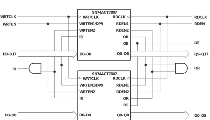
The SN74ACT7807 is a 2048-word by 9-bit FIFO with high speed and fast access times. It processes data at
rates up to 67 MHz and access times of 12 ns in a bit-parallel format. Data outputs are noninverting with respect
to the data inputs. Expansion is easily accomplished in both word width and word depth.
The write-clock (WRTCLK) and read-clock (RDCLK) inputs should be free running and can be asynchronous
or coincident. Data is written to memory on the rising edge of WRTCLK when the write-enable (WRTEN1/DP9,
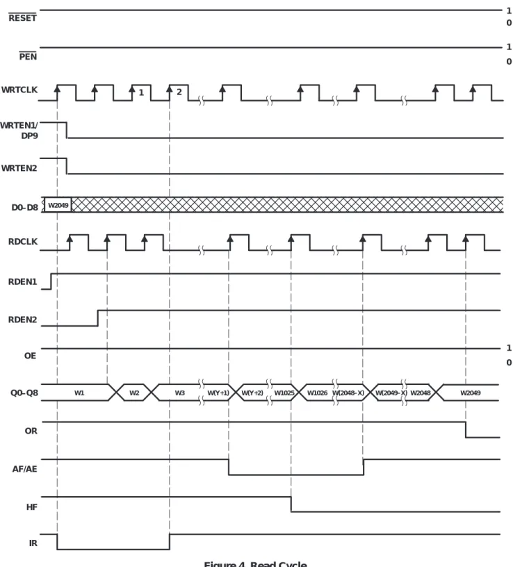
WRTEN2) inputs are high and the input-ready (IR) flag output is high. Data is read from memory on the rising
edge of RDCLK when the read-enable (RDEN1, RDEN2) and output-enable (OE) inputs are high and the
output-ready (OR) flag output is high. The first word written to memory is clocked through to the output buffer
regardless of the levels on RDEN1, RDEN2, and OE. The OR flag indicates that valid data is present on the
output buffer.
The FIFO can be reset asynchronous to WRTCLK and RDCLK. RESET must be asserted while at least four
WRTCLK and four RDCLK cycles occur to clear the synchronizing registers. Resetting the FIFO initializes the
IR, OR, and half-full (HF) flags low and the almost-full/almost-empty (AF/AE) flag high. The FIFO must be reset
upon power up.
Q1 VCC Q2 Q3 GND Q4 VCC Q5 Q6 GND Q7 39 38 37 36 35 34 33 32 31 30 29 18 19 7 8 9 10 11 12 13 14 15 16 17 D0 D1 D2 GND D3 D4 D5 VCC D6 D7 D8 20 21 22 23 FN PACKAGE (TOP VIEW) NC OE GND Q0 5 4 3 2 1 6 44
HF AF/AE GND PEN RESET
RDEN1 RDCLK Q8 GND WR TCLK WR TEN1/DP9 WR TEN2 IR OR RDEN2 42 41 40 43 24 25 26 27 28 VCC VCC VCC Q2 Q3 GND GND Q4 Q5 Q6 GND GND Q7 NC V CC V CC V CC V CC 64 63 62 61 60 59 58 57 56 55 54 53 52 51 50 49 Q1 PAG OR PM PACKAGE (TOP VIEW) NC Q0 GND GND OE NC VCC VCC RESET PEN GND GND AF/AE HF VCC NC Q8 VCC VCC RDCLK RDEN1 NC RDEN2 OR IR WRTEN2 WRTEN1/DP9 WRTCLK GND GND 1 2 3 4 5 6 7 8 9 10 11 12 13 14 15 48 47 46 45 44 43 42 41 40 39 38 37 36 35 34
logic symbol
†
WRTEN & RDEN & 0 7 D0 8 D1 9 D2 11 D3 12 D4 13 D5 15 D6 16 D7 8 17 D8 Q0 40 0 Q1 39 Q2 37 Q3 36 Q4 34 IR 22 IN RDY HF 5 HALF FULL AF/AE 4 ALMOST FULL/EMPTY OR 23 OUT RDY Q5 32 Q6 31 Q7 29 Q8 28 8 Data 1 RESET 25 RDEN1 EN1 42 OE PEN RESET 1 19 WRTCLK WRTCLK 20 WRTEN1/DP9 21 WRTEN2 2 26 RDCLK RDCLK PROGRAM ENABLE 24 RDEN2 Data Φ FIFO 2048 × 9 SN74ACT7807† This symbol is in accordance with ANSI/IEEE Std 91-1984 and IEC Publication 617-12. Pin numbers shown are for the FN package.
functional block diagram
Q0 – Q8 OR IR AF/AE HF Register 2048 × 9 RAM OE D0–D8 RDCLK RDEN1 RDEN2 WRTCLK WRTEN1/DP9 WRTEN2 RESET PEN Synchronous Read Control Synchronous Write Control Reset Logic Write Pointer Status-Flag Logic Location 1 Location 2 Location 2047 Location 2048 Read PointerTerminal Functions
TERMINAL
NAME I/O DESCRIPTION
AF/AE O
Almost-full/almost-empty flag. Depth offset values can be programmed for AF/AE or the default value of 256 can be used for both the almost-empty offset (X) and the almost-full offset (Y). AF/AE is high when memory contains X or fewer words or (2048 – Y) or more words. AF/AE is high after reset.
D0–D8 I Nine-bit data input port
HF O Half-full flag. HF is high when the FIFO memory contains 1024 or more words. HF is low after reset.
IR O
Input-ready flag. IR is synchronized to the low-to-high transition of WRTCLK. When IR is low, the FIFO is full and writes are disabled. IR is low during reset and goes high on the second low-to-high transition of WRTCLK after reset.
OE I Output enable. When OE, RDEN1, RDEN2 and OR are high, data is read from the FIFO on a low-to-high transition of RDCLK. When OE is low, reads are disabled and the data outputs are in the high-impedance state.
OR O
Output-ready flag. OR is synchronized to the low-to-high transition of RDCLK. When OR is low, the FIFO is empty and reads are disabled. Ready data is present on Q0–Q17 when OR is high. OR is low during reset and goes high on the third low-to-high transition of RDCLK after the first word is loaded to empty memory.
PEN I Program enable. After reset and before the first word is written to the FIFO, the binary value on D0–D8 and DP9 is latched as an AF/AE offset value when PEN is low and WRTCLK is high.
Q0–Q8 O
Nine-bit data output port. After the first valid write to empty memory, the first word is output on Q0–Q8 on the third rising edge of RDCLK. OR also is asserted high at this time to indicate ready data. When OR is low, the last word read from the FIFO is present on Q0–Q8.
RDCLK I
Read clock. RDCLK is a continuous clock and can be asynchronous or coincident to WRTCLK. A low-to-high transition of RDCLK reads data from memory when RDEN1, RDEN2, OE, and OR are high. OR is synchronous to the low-to-high transition of RDCLK.
RDEN1
RDEN2 I
Read enables. When RDEN1, RDEN2, OE, and OR are high, data is read from the FIFO on the low-to-high transition of RDCLK.
RESET I Reset. To reset the FIFO, four low-to-high transitions of RDCLK and four low-to-high transitions of WRTCLK must occur while RESET is low. This sets HF, IR, and OR low and AF/AE high.
WRTCLK I
Write clock. WRTCLK is a continuous clock and can be asynchronous or coincident to RDCLK. A low-to-high transition of WRTCLK writes data to memory when WRTEN1/DP9, WRTEN2, and IR are high. IR is synchronous to the low-to-high transition of WRTCLK.
WRTEN1/DP9 I
Write enable/data pin 9. When WRTEN1/DP9, WRTEN2, and IR are high, data is written to the FIFO on a low-to-high transition of WRTCLK. When programming an AF/AE offset value, WRTEN1/DP9 is used as the most-significant data bit.
WRTEN2 I Write enable. When WRTEN1/DP9, WRTEN2, and IR are high, data is written to the FIFO on a low-to-high transition of WRTCLK.
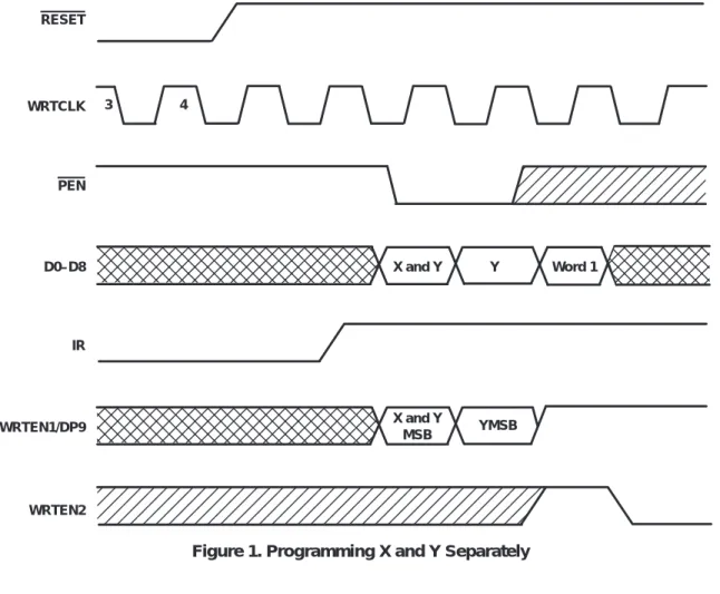
offset values for AF/AE
The AF/AE flag has two programmable limits: the almost-empty offset value (X) and the almost-full offset
value (Y). They can be programmed after the FIFO is reset and before the first word is written to memory. If the
offsets are not programmed, the default values of X = Y = 256 are used. The AF/AE flag is high when the FIFO
contains X or fewer words or (2048 – Y) or more words.
Program enable (PEN) should be held high throughout the reset cycle. PEN can be brought low only when IR
is high and WRTCLK is low. On the following low-to-high transition of WRTCLK, the binary value on D0–D8 and
WRTEN1/DP9 is stored as the almost-empty offset value (X) and the almost-full offset value (Y). Holding PEN
low for another low-to-high transition of WRTCLK reprograms Y to the binary value on D0–D8 and
WRTEN1/DP9 at the time of the second WRTCLK low-to-high transition. While the offsets are programmed,
data is not written to the FIFO memory, regardless of the state of the write enables (WRTEN1/DP9, WRTEN2).
A maximum value of 1023 can be programmed for either X or Y (see Figure 1). To use the default values of
X = Y = 256, PEN must be held high.
X and Y MSB ÎÎÎÎÎÎÎÎÎÎÎÎ ÎÎÎÎÎÎÎÎÎÎÎÎ ÎÎÎÎÎÎÎÎÎÎÎÎ ÎÎÎÎÎ ÎÎÎÎÎ 3 4 RESET ÎÎÎÎÎÎÎÎÎÎÎ ÎÎÎÎÎÎÎÎÎÎÎ PEN D0–D8 WRTCLK WRTEN1/DP9 WRTEN2 IR X and Y Y YMSB ÏÏÏÏÏÏÏÏÏÏÏÏÏÏÏÏÏÏ ÏÏÏÏÏÏÏÏÏÏÏÏÏÏÏÏÏÏ ÏÏÏÏÏÏÏÏÏÏÏÏÏÏÏÏÏÏ Word 1 ÏÏÏÏÏÏÏÏ ÏÏÏÏÏÏÏÏ
ÉÉÉÉÉÉÉÉÉÉÉÉÉÉÉÉÉÉÉÉÉÉÉÉÉÉÉÉÉÉ ÉÉÉÉÉÉÉÉÉÉÉÉÉÉÉÉÉÉÉÉÉÉÉÉÉÉÉÉÉÉ ÎÎÎÎÎÎÎÎÎÎÎÎÎÎÎÎÎÎÎ ÎÎÎÎÎÎÎÎÎÎÎÎÎÎÎÎÎÎÎ 1 2 3 4 1 2 ÎÎÎÎÎÎÎÎÎÎÎÎÎÎÎÎÎÎÎ ÎÎÎÎÎÎÎÎÎÎÎÎÎÎÎÎÎÎÎ Don’t Care Don’t Care ÎÎÎÎÎÎÎÎÎÎÎÎÎÎÎÎÎÎÎÎÎÎÎÎÎÎÎÎÎÎ ÎÎÎÎÎÎÎÎÎÎÎÎÎÎÎÎÎÎÎÎÎÎÎÎÎÎÎÎÎÎ Don’t Care 1 2 3 4 ÎÎÎÎÎÎÎÎÎÎÎÎÎÎÎÎÎÎÎ ÎÎÎÎÎÎÎÎÎÎÎÎÎÎÎÎÎÎÎ Don’t Care ÎÎÎÎÎÎÎÎÎÎÎÎÎÎÎÎÎÎÎ ÎÎÎÎÎÎÎÎÎÎÎÎÎÎÎÎÎÎÎ ÎÎÎÎÎÎÎÎÎÎÎÎÎÎÎÎÎÎÎ Don’t Care Invalid ÎÎÎÎÎÎÎÎÎÎÎÎÎ ÎÎÎÎÎÎÎÎÎÎÎÎÎ ÎÎÎÎÎÎÎÎÎÎÎÎÎ Don’t Care ÎÎÎÎÎÎ ÎÎÎÎÎÎ Don’t Care ÎÎÎÎÎÎ ÎÎÎÎÎÎ Don’t Care ÎÎÎÎÎÎÎÎÎÎÎ ÎÎÎÎÎÎÎÎÎÎÎ Don’t Care RESET WRTCLK PEN WRTEN1/DP9 WRTEN2 D0–D8 RDCLK RDEN1 OE RDEN2 Q0–Q8 OR AF/AE HF IR
Define the AF/AE Flag Using the Default Value of X = Y = 256
1 0
1 0
ÉÉÉÉÉÉÉÉÉÉÉÉÉÉÉÉÉÉÉÉÉÉÉÉÉÉÉÉ ÉÉÉÉÉÉÉÉÉÉÉÉÉÉÉÉÉÉÉÉÉÉÉÉÉÉÉÉ ÎÎÎÎÎÎÎÎÎÎÎÎÎÎÎÎÎÎÎÎÎÎÎÎÎÎÎÎ 1 2 3 Invalid RESET WRTCLK PEN WRTEN1/DP9 WRTEN2 D0–D8 RDCLK RDEN1 OE RDEN2 Q0–Q8 OR AF/AE HF IR 1 0 1 0 1 0 W1 W2 W3 W4 W(X+2) W1025 W(2049–Y) W2049 1 0 1 0 W1
ÉÉÉÉÉÉÉÉÉÉÉÉÉÉÉÉÉÉÉÉÉÉÉÉÉÉÉÉÉ ÉÉÉÉÉÉÉÉÉÉÉÉÉÉÉÉÉÉÉÉÉÉÉÉÉÉÉÉÉ W1026 ÎÎÎÎÎÎÎÎÎÎÎÎÎÎÎÎÎÎÎÎÎÎÎÎÎÎÎÎÎÎ ÎÎÎÎÎÎÎÎÎÎÎÎÎÎÎÎÎÎÎÎÎÎÎÎÎÎÎÎÎÎ RESET WRTCLK PEN WRTEN1/ DP9 WRTEN2 D0–D8 RDCLK RDEN1 OE RDEN2 Q0–Q8 OR AF/AE HF IR 1 0 1 0 W2049 1 2 W1 W2 W3 W(Y+1) W(Y+2) W1025 W(2048–X) W(2049–X) W2048 W2049 1 0
absolute maximum ratings over operating free-air temperature range (unless otherwise noted)
†
Supply voltage range, V
CC. . .
–0.5 V to 7 V
Input voltage range, V
I. . .
–0.5 V to 7 V
Voltage range applied to a disabled 3-state output
. . .
–0.5 V to 5.5 V
Package thermal impedance,
θ
JA(see Note 1): FN package
. . .
46
°
C/W
PAG package
. . .
58
°
C/W
PM package
. . .
67
°
C/W
Storage temperature range, T
stg–65
. . .
°
C to 150
°
C
† Stresses beyond those listed under “absolute maximum ratings” may cause permanent damage to the device. These are stress ratings only, and functional operation of the device at these or any other conditions beyond those indicated under “recommended operating conditions” is not implied. Exposure to absolute-maximum-rated conditions for extended periods may affect device reliability.
NOTE 1: The package thermal impedance is calculated in accordance with JESD 51.
recommended operating conditions
’ACT7807-15 ’ACT7807-20 ’ACT7807-25 ’ACT7807-40 UNIT MIN MAX MIN MAX MIN MAX MIN MAX UNIT
VCC Supply voltage 4.5 5.5 4.5 5.5 4.5 5.5 4.5 5.5 V
VIH High-level input voltage 2 2 2 2 V
VIL Low-level input voltage 0.8 0.8 0.8 0.8 V
IOH High-level output current Q outputs, flags –8 –8 –8 –8 mA
IOL Low level output current Q outputs 16 16 16 16 mA
IOL Low-level output current
Flags 8 8 8 8 mA
TA Operating free-air temperature 0 70 0 70 0 70 0 70 °C
electrical characteristics over recommended operating free-air temperature range (unless
otherwise noted)
PARAMETER TEST CONDITIONS MIN TYP‡ MAX UNIT
VOH VCC = 4.5 V, IOH = –8 mA 2.4 V
VOL Flags VCC = 4.5 V, IOL = 8 mA 0.5 V
VOL
Q outputs VCC = 4.5 V, IOL = 16 mA 0.5 V
II VCC = 5.5 V, VI = VCC or 0 ±5 µA
IOZ VCC = 5.5 V, VO = VCC or 0 ±5 µA
ICC VCC = 5.5 V, VI = VCC – 0.2 V or 0 400 µA
∆ICC§ WRTEN1/DP9 VCC = 5 5 V One input at 3 4 V Other inputs at VCC or GND 2 mA
∆ICC§ Other inputs VCC = 5.5 V, One input at 3.4 V, Other inputs at VCC or GND
1 mA
Ci VI = 0, f = 1 MHz 4 pF
Co VO = 0, f = 1 MHz 8 pF
‡ All typical values are at VCC = 5 V, TA = 25°C.
timing requirements over recommended operating free-air temperature range (unless otherwise
noted) (see Figures 1 through 5)
’ACT7807-15 ’ACT7807-20 ’ACT7807-25 ’ACT7807-40 UNIT MIN MAX MIN MAX MIN MAX MIN MAX UNIT
fclock Clock frequency 67 50 40 25 MHz
WRTCLK high or low 6 8 9 13
tw Pulse duration RDCLK high or low 6 8 9 13 ns
PEN low 6 9 9 13
D0–D8 before WRTCLK↑ 4 5 5 5
WRTEN1, WRTEN2
before WRTCLK↑ 4 5 5 5
tsu Setup time OE, RDEN1, RDEN2before RDCLK↑ 5 6 6 6.5 ns
Reset: RESET low before
first WRTCLK↑ and RDCLK↑† 7 8 8 8 PEN before WRTCLK↑ 4 5 5 5 D0–D8 after WRTCLK↑ 0 0 0 0 WRTEN1, WRTEN2 after WRTCLK↑ 0 0 0 0 th Hold time
OE, RDEN1, RDEN2
after RDCLK↑ 0 0 0 0 ns
h
Reset: RESET low after
fourth WRTCLK↑ and RDCLK↑† 5 5 5 5
PEN high after WRTCLK↓ 0 0 0 0
PEN low after WRTCLK↑ 3 3 3 3
† To permit the clock pulse to be utilized for reset purposes
switching characteristics over recommended ranges of supply voltage and operating free-air
temperature, C
L
= 50 pF (unless otherwise noted) (see Figure 5)
PARAMETER FROM TO ’ACT7807-15 ’ACT7807-20 ’ACT7807-25 ’ACT7807-40 UNIT PARAMETER
(INPUT) (OUTPUT) MIN TYP‡ MAX MIN MAX MIN MAX MIN MAX UNIT
fmax WRTCLK orRDCLK 67 50 40 25 MHz tpd RDCLK↑ Any Q 3 9 12 3 13 3 18 3 25 ns tpd§ RDCLK↑ Any Q 8 ns WRTCLK↑ IR 1 9 1 12 1 14 1 16 t d RDCLK↑ OR 1 9 2 12 2 14 2 16 ns tpd WRTCLK↑ AF/AE 2 16 2 20 2 25 2 30 ns RDCLK↑ AF/AE 2 17 2 20 2 25 2 30 tPLH WRTCLK↑ HF 2 19 2 21 2 23 2 25 ns tPHL RDCLK↑ HF 2 16 2 18 2 20 2 22 ns
tPLH RESET low AF/AE 1 12 1 18 1 22 1 24 ns
tPHL RESET low HF 2 12 2 18 2 22 2 24 ns
ten OE Any Q 2 10 2 13 2 15 2 18 ns
tdis OE Any Q 1 11 1 13 1 15 1 18 ns
operating characteristics, V
CC
= 5 V, T
A
= 25
°
C
PARAMETER TEST CONDITIONS TYP UNIT
Cpd Power dissipation capacitance per FIFO channel Outputs enabled CL = 50 pF, f = 5 MHz 91 pF
PARAMETER MEASUREMENT INFORMATION
VOH VOL th tPLH tPHL Output Control Output Waveform 1 S1 at 7 V Output Waveform 2 S1 at Open tPZL tPZH tPLZ tPHZ 1.5 V 1.5 V 1.5 V 1.5 V 3 V 0 V 1.5 V 1.5 V VOH VOL 0 V 1.5 V VOL + 0.3 V 1.5 V VOH – 0.3 V ≈0 V 1.5 V 3 V 0 V 1.5 V 1.5 V 0 V 3 V 0 V 1.5 V 1.5 V tw Input 3 V 3 V ≈3.5 V VOLTAGE WAVEFORMS
SETUP AND HOLD TIMES
VOLTAGE WAVEFORMS PROPAGATION DELAY TIMES
VOLTAGE WAVEFORMS PULSE DURATION
VOLTAGE WAVEFORMS ENABLE AND DISABLE TIMES Timing Input Data Input Output Input S1 500 Ω LOAD CIRCUIT 500 Ω 7 V From Output Under Test Test Point
NOTE A: CL includes probe and jig capacitance.
CL = 50 pF (see Note A) tsu tPZH tPZL tPHZ tPLZ tPLH tPHL Open Closed Open Closed Open Open PARAMETER S1 ten tdis tpd
TYPICAL CHARACTERISTICS
Figure 6
PROPAGATION DELAY TIME vs LOAD CAPACITANCE 0 50 100 150 200 250 300 CL – Load Capacitance – pF VCC = 5 V RL = 500 Ω TA = 25°C pd t – Propagation Delay T ime – ns typ + 8 typ + 6 typ + 4 typ + 2 typ typ – 2
Figure 7
– Active I CC(f) I CC – mA 100 80 40 20 0 60 0 10 20 30 40 50 60 120 70 ACTIVE ICC vs FREQUENCY f – Frequency – MHz 140 160 180 200 TA = 25°C VCC = 5 V VCC = 4.5 V VCC = 5.5 V 5 4 2 1 0 3 0 10 20 30 40 50 60 6 f – Frequency – MHz 70 Slope = 0.07 VCC = 4.5 V VCC = 5 V VCC = 5.5 V TA = 25° – Idle I CC(I) I CC – mAFigure 8. SN74ACT7807 Idle I
CCWith WRTCLK Switching,
Other Inputs at 0 or V
CC– 0.2 V and Outputs Disconnected
APPLICATION INFORMATION
WRTCLK WRTEN1/DP9 WRTEN1 WRTEN2 WRTEN2 IR IR WRTCLK D0–D8 RDCLK OR RDEN1 RDEN2 OE RDCLK WRTEN1/DP9 WRTEN2 IR RDEN1 RDEN1 OR OR OE OE Q0–Q8 5 V RDEN2 RDEN2 CLOCK D0–D8 Q0–Q8 D0–D8 Q0–Q8 SN74ACT7807 SN74ACT7807 WRTCLK RDCLKFigure 9. Word-Depth Expansion: 4096
×
9 Bits
WRTEN1/DP9 WRTEN2 IR OE RDEN1 RDEN2 OR WRTEN1/DP9 WRTEN2 IR D0–D8 OE RDEN1 RDEN2 OR WRTCLK WRTEN D9–D17 IR D0–D8 RDCLK RDEN Q9–Q17 OR OE D0–D8 Q0–Q8 Q0–Q8 Q0–Q8 SN74ACT7807 SN74ACT7807 WRTCLK RDCLK WRTCLK RDCLK
www.ti.com 17-Dec-2015
PACKAGING INFORMATION
Orderable Device Status
(1)
Package Type Package Drawing Pins Package Qty Eco Plan (2) Lead/Ball Finish (6) MSL Peak Temp (3)
Op Temp (°C) Device Marking
(4/5)
Samples
SN74ACT7807-15PM OBSOLETE LQFP PM 64 TBD Call TI Call TI 0 to 70
SN74ACT7807-20FN ACTIVE PLCC FN 44 26 Green (RoHS
& no Sb/Br)
CU NIPDAU Level-3-260C-168 HR 0 to 70 SN74
ACT7807-20FN
SN74ACT7807-20PM OBSOLETE LQFP PM 64 TBD Call TI Call TI 0 to 70
SN74ACT7807-25PM OBSOLETE LQFP PM 64 TBD Call TI Call TI 0 to 70
SN74ACT7807-40PM OBSOLETE LQFP PM 64 TBD Call TI Call TI 0 to 70
(1)
The marketing status values are defined as follows:
ACTIVE: Product device recommended for new designs.
LIFEBUY: TI has announced that the device will be discontinued, and a lifetime-buy period is in effect.
NRND: Not recommended for new designs. Device is in production to support existing customers, but TI does not recommend using this part in a new design. PREVIEW: Device has been announced but is not in production. Samples may or may not be available.
OBSOLETE: TI has discontinued the production of the device.
(2)
Eco Plan - The planned eco-friendly classification: Pb-Free (RoHS), Pb-Free (RoHS Exempt), or Green (RoHS & no Sb/Br) - please check http://www.ti.com/productcontent for the latest availability
information and additional product content details.
TBD: The Pb-Free/Green conversion plan has not been defined.
Pb-Free (RoHS): TI's terms "Lead-Free" or "Pb-Free" mean semiconductor products that are compatible with the current RoHS requirements for all 6 substances, including the requirement that
lead not exceed 0.1% by weight in homogeneous materials. Where designed to be soldered at high temperatures, TI Pb-Free products are suitable for use in specified lead-free processes.
Pb-Free (RoHS Exempt): This component has a RoHS exemption for either 1) lead-based flip-chip solder bumps used between the die and package, or 2) lead-based die adhesive used between
the die and leadframe. The component is otherwise considered Pb-Free (RoHS compatible) as defined above.
Green (RoHS & no Sb/Br): TI defines "Green" to mean Pb-Free (RoHS compatible), and free of Bromine (Br) and Antimony (Sb) based flame retardants (Br or Sb do not exceed 0.1% by weight
in homogeneous material)
(3)
MSL, Peak Temp. - The Moisture Sensitivity Level rating according to the JEDEC industry standard classifications, and peak solder temperature.
(4)
There may be additional marking, which relates to the logo, the lot trace code information, or the environmental category on the device.
(5)
www.ti.com 17-Dec-2015
Important Information and Disclaimer:The information provided on this page represents TI's knowledge and belief as of the date that it is provided. TI bases its knowledge and belief on information
provided by third parties, and makes no representation or warranty as to the accuracy of such information. Efforts are underway to better integrate information from third parties. TI has taken and continues to take reasonable steps to provide representative and accurate information but may not have conducted destructive testing or chemical analysis on incoming materials and chemicals. TI and TI suppliers consider certain information to be proprietary, and thus CAS numbers and other limited information may not be available for release.
FN (S-PQCC-J**)
PLASTIC J-LEADED CHIP CARRIER
4040005 / B 03/95 20 PIN SHOWN 0.026 (0,66) 0.032 (0,81) D2 / E2 0.020 (0,51) MIN 0.180 (4,57) MAX 0.120 (3,05) 0.090 (2,29) D2 / E2 0.013 (0,33) 0.021 (0,53) Seating Plane MAX D2 / E2 0.219 (5,56) 0.169 (4,29) 0.319 (8,10) 0.469 (11,91) 0.569 (14,45) 0.369 (9,37) MAX 0.356 (9,04) 0.456 (11,58) 0.656 (16,66) 0.008 (0,20) NOM 1.158 (29,41) 0.958 (24,33) 0.756 (19,20) 0.191 (4,85) 0.141 (3,58) MIN 0.441 (11,20) 0.541 (13,74) 0.291 (7,39) 0.341 (8,66) 18 19 14 13 D D1 1 3 9 E1 E 4 8 MIN MAX MIN PINS ** 20 28 44 0.385 (9,78) 0.485 (12,32) 0.685 (17,40) 52 68 84 1.185 (30,10) 0.985 (25,02) 0.785 (19,94) D / E 0.395 (10,03) 0.495 (12,57) 1.195 (30,35) 0.995 (25,27) 0.695 (17,65) 0.795 (20,19) NO. OF D1 / E1 0.350 (8,89) 0.450 (11,43) 1.150 (29,21) 0.950 (24,13) 0.650 (16,51) 0.750 (19,05) 0.004 (0,10) M 0.007 (0,18) 0.050 (1,27)NOTES: A. All linear dimensions are in inches (millimeters). B. This drawing is subject to change without notice. C. Falls within JEDEC MS-018
PM (S-PQFP-G64)
PLASTIC QUAD FLATPACK
4040152 / C 11/96 32 17 0,13 NOM 0,25 0,45 0,75 Seating Plane 0,05 MIN Gage Plane 0,27 33 16 48 1 0,17 49 64 SQ SQ 10,20 11,80 12,20 9,80 7,50 TYP 1,60 MAX 1,45 1,35 0,08 0,50 0,08 M 0°– 7°NOTES: A. All linear dimensions are in millimeters. B. This drawing is subject to change without notice. C. Falls within JEDEC MS-026
complete. All semiconductor products (also referred to herein as “components”) are sold subject to TI’s terms and conditions of sale supplied at the time of order acknowledgment.
TI warrants performance of its components to the specifications applicable at the time of sale, in accordance with the warranty in TI’s terms and conditions of sale of semiconductor products. Testing and other quality control techniques are used to the extent TI deems necessary to support this warranty. Except where mandated by applicable law, testing of all parameters of each component is not necessarily performed.
TI assumes no liability for applications assistance or the design of Buyers’ products. Buyers are responsible for their products and applications using TI components. To minimize the risks associated with Buyers’ products and applications, Buyers should provide adequate design and operating safeguards.
TI does not warrant or represent that any license, either express or implied, is granted under any patent right, copyright, mask work right, or other intellectual property right relating to any combination, machine, or process in which TI components or services are used. Information published by TI regarding third-party products or services does not constitute a license to use such products or services or a warranty or endorsement thereof. Use of such information may require a license from a third party under the patents or other intellectual property of the third party, or a license from TI under the patents or other intellectual property of TI.
Reproduction of significant portions of TI information in TI data books or data sheets is permissible only if reproduction is without alteration and is accompanied by all associated warranties, conditions, limitations, and notices. TI is not responsible or liable for such altered documentation. Information of third parties may be subject to additional restrictions.
Resale of TI components or services with statements different from or beyond the parameters stated by TI for that component or service voids all express and any implied warranties for the associated TI component or service and is an unfair and deceptive business practice. TI is not responsible or liable for any such statements.
Buyer acknowledges and agrees that it is solely responsible for compliance with all legal, regulatory and safety-related requirements concerning its products, and any use of TI components in its applications, notwithstanding any applications-related information or support that may be provided by TI. Buyer represents and agrees that it has all the necessary expertise to create and implement safeguards which anticipate dangerous consequences of failures, monitor failures and their consequences, lessen the likelihood of failures that might cause harm and take appropriate remedial actions. Buyer will fully indemnify TI and its representatives against any damages arising out of the use of any TI components in safety-critical applications.
In some cases, TI components may be promoted specifically to facilitate safety-related applications. With such components, TI’s goal is to help enable customers to design and create their own end-product solutions that meet applicable functional safety standards and requirements. Nonetheless, such components are subject to these terms.
No TI components are authorized for use in FDA Class III (or similar life-critical medical equipment) unless authorized officers of the parties have executed a special agreement specifically governing such use.
Only those TI components which TI has specifically designated as military grade or “enhanced plastic” are designed and intended for use in military/aerospace applications or environments. Buyer acknowledges and agrees that any military or aerospace use of TI components
which havenotbeen so designated is solely at the Buyer's risk, and that Buyer is solely responsible for compliance with all legal and
regulatory requirements in connection with such use.
TI has specifically designated certain components as meeting ISO/TS16949 requirements, mainly for automotive use. In any case of use of non-designated products, TI will not be responsible for any failure to meet ISO/TS16949.
Products Applications
Audio www.ti.com/audio Automotive and Transportation www.ti.com/automotive
Amplifiers amplifier.ti.com Communications and Telecom www.ti.com/communications
Data Converters dataconverter.ti.com Computers and Peripherals www.ti.com/computers
DLP® Products www.dlp.com Consumer Electronics www.ti.com/consumer-apps
DSP dsp.ti.com Energy and Lighting www.ti.com/energy
Clocks and Timers www.ti.com/clocks Industrial www.ti.com/industrial
Interface interface.ti.com Medical www.ti.com/medical
Logic logic.ti.com Security www.ti.com/security
Power Mgmt power.ti.com Space, Avionics and Defense www.ti.com/space-avionics-defense
Microcontrollers microcontroller.ti.com Video and Imaging www.ti.com/video
RFID www.ti-rfid.com