Method to determine defect positions below a metal surface by STM
Ye. S. Avotina,1,2Yu. A. Kolesnichenko,1 A. N. Omelyanchouk,1A. F. Otte,2and J. M. van Ruitenbeek2 1B.I. Verkin Institute for Low Temperature Physics and Engineering, National Academy of Sciences of Ukraine, 47, Lenin Ave., 61103,
Kharkov, Ukraine
2Kamerlingh Onnes Laboratorium, Universiteit Leiden, Postbus 9504, 2300 Leiden, The Netherlands 共Received 24 September 2004; published 29 March 2005兲
The oscillatory voltage dependence of the conductance of a quantum point contact in the presence of a single pointlike defect has been analyzed theoretically. Such signals are detectable and may be exploited to obtain information on defect positions below a metal surface. Both tunnel junctions and ballistic contacts of adiabatic shape have been considered. The effect of quantum interference has been taken into account between the principal wave that is directly transmitted through the contact and the partial wave that is scattered by the contact and the defect. This effect leads to oscillations of the conductance as a function of applied voltage. We obtain the dependence of the period and amplitude of the conductance oscillations on the position of the defect inside the metal.
DOI: 10.1103/PhysRevB.71.115430 PACS number共s兲: 73.23.⫺b, 72.10.Fk
I. INTRODUCTION
In the two decades following its invention, scanning tun-neling microscopy共STM兲 has proved to be a valuable tool for investigating surfaces on an atomic scale. More recently, several experiments show a growing interest in the study of structures that are situated in the bulk below the surface in both semiconductors and metals. Whereas in the former共i.e., semiconductor兲 case the absence of effective screening al-lows dopants down to the third subsurface layer to be viewed directly as apparent topographic features,1 the situation for metals turns out to be somewhat more complicated. One method that has been suggested for imaging structures buried in metal involves several surface study techniques to be em-ployed simultaneously in combination with STM.2However, although this experiment has lead to successful identification of subsurface defects, it cannot be used as a tool for probing the exact depth. Also, its employability is limited to certain specific alloys only. A more successful approach, however, seems to be by probing standing electron waves.3,4 The groundwork of these experiments is as described in Ref. 5, where Cu共111兲surface states form a two-dimensional nearly free electron gas. When scattered from step edges or ada-toms, these states then form standing waves that can be probed by scanning tunneling spectroscopy共STS兲.
Although it has been proposed to utilize these surface states for imaging subsurface impurities,6the exponential de-cay of the wave-function amplitudes into the bulk will limit the effective range to the topmost layers only. Bulk states, however, of which the square falls off with only r2, form a good alternative. To demonstrate this, we mention results that were obtained by bulk state spectroscopy on relatively large structures, such as Ar bubbles submerged in Al共Ref. 3兲 and Si共111兲 step edges buried under a thin film of Pb.4 In these experiments, bulk electrons are found to be confined in a vertical quantum well between the surface and the top plane of the object of interest.
In this paper we show that the investigation of the non-linear conductance of a point contact placed on a metal sur-face makes it possible to determine the position of pointlike
defects, such as the vacancies or foreign atoms inside the metal in the vicinity of the contact. We consider theoretical models both for the cases of a tunnel point contact and for a ballistic quantum contact. We look for conductance oscilla-tions caused by interference of electrons that are transmitted directly, and electrons that are first backscattered elastically by the defect and again scattered forward by the contact共i.e., the tip-sample junction兲, much in the same way as was de-scribed for atomic point contacts in Refs. 7–9. The effect of such quantum interference on the nonlinear conductance of quantum wires was theoretically analyzed in Refs. 11–13, but the point-contact geometry was not yet studied.
The organization of this paper is as follows. In Sec. II we consider a tunnel junction in the limit of a high potential barrier. The interaction of the transmitted electrons with a single impurity near the junction is taken into account by perturbation theory with the electron-impurity interaction as the small parameter. A general analytical expression for the voltage dependence of conductance G共V兲 is obtained. It de-fines G共V兲 in terms of the contact diameter, the distance between contact and the impurity and the parameters that characterize the metal, and the transmission of the tunnel junction. In Sec. III the conductance of a ballistic quantum contact of adiabatic shape is analyzed. In absence of a barrier inside the contact, electrons can still be reflected from it due to the variation of the confining potential. The influence on electron scattering by an explicit barrier potential in the cen-ter of the contact is also discussed. As in Sec. II, assuming the electron-impurity interaction to be small, we derive an expression for G共V兲 and its dependence on the position of the defect. In Sec. IV we conclude by discussing the possi-bilities for experimental exploitation of the conductance fluc-tuations for subsurface imaging as well as the technical dif-ficulties involved.
II. TUNNEL POINT CONTACT
half-spaces in which there is an orifice共contact兲, as illustrated in Fig. 1. The potential barrier in the plane z = 0 is taken to be a ␦function
U共r兲= Uf共兲␦共z兲, 共1兲
where =共x , y兲 is a two-dimensional vector. The function f共兲→⬁in all points of the plane z = 0 except in the contact, where f共兲= 1. At a point r = r0in vicinity of the interface, in the half-space z⬎0, a pointlike defect is placed共see Fig. 1兲. The electron interaction with the defect is described by the potential
g共r兲= g␦共r − r0兲, 共2兲 where g is the constant of the electron-impurity interaction. In this section we consider tunnel junctions and assume that the transmission probability of electrons through the orifice is small. In that case the applied voltage drops entirely over the barrier and we choose the electric potential as a step function V共z兲= V⌰共−z兲and take eV⬎0.
The electrical current I共V兲 can be evaluated10 from the electron wave functions of the systemk,
I共V兲= eប
43m*
冕
dk冕
dS Im共k *ⵜk兲⌰共kz兲关nF共k兲− nF共k
+ eV兲兴. 共3兲
Here,k=ប2k2/ 2m*is the electron energy, k is the electron wave vector, m*is an effective mass of electron, and n
F共k兲
is the Fermi distribution function. The real-space integration is performed over a surface overlapping the contacts in the region z⬎0. At low temperatures the tunnel current is due to those electrons in the half-space z⬍0 having an energy be-tween the Fermi energyF andF+ eV because, on the other
side of the barrier, only states withk艌Fare available. The wave functionksatisfies the Schrödinger equation
ⵜ2
k共,z兲+
2m*
ប2 关k− U共r兲− g共r兲− eV共z兲兴k共,z兲= 0,
共4兲
where the wave vector k =共⑂, kz兲 has components ⑂ and kz
parallel and perpendicular to interface, respectively. As shown in Ref. 14, Eq.共4兲can be solved for arbitrary form of the function f共兲 in the limit 1 / U→0. The wave function k共, z兲 for kz⬎0 in the main approximation of the small
parameter⬃1 / U takes the form
˜k共,z兲= ei⑂共eik˜z− e−ik˜z兲+
1 Uk˜
共−兲
共,z兲 共z⬍0兲, 共5兲
k共,z兲=
1 Uk
共+兲共
,z兲 共z⬎0兲, 共6兲
where k˜ =共⑂, −k˜兲, k˜ =
冑
kz2+ 2meV /ប2. The function k共, z兲
satisfies the conditions of continuity and the condition of the jump of its derivative at the boundary z = 0. At large U these conditions are reduced to
k˜
共−兲
共,0兲=k共+兲共,0兲, 共7兲
ik˜ =m *
ប2f共兲k共
+兲共,0兲. 共8兲
In the absence of the defect共g = 0兲 the wave function was obtained in Ref. 14,
0k共 +兲共
,z兲= − iប 2˜k 2m*
冕
−⬁⬁
d⑂
⬘
F共⑂−⑂⬘
兲ei⑂⬘+ikz⬘z, 共9兲 whereF共⑂−⑂
⬘
兲=冕
−⬁⬁ de
i共⑂−⑂⬘兲
f共兲 共10兲
and kz
⬘
=冑
⑂2+ kz2−⑂⬘
2. For a circular contact of a radius a, defined by f共兩兩艋a兲= 1 and f共兩兩⬎a兲→⬁, the function F共⑂−⑂⬘
兲takes the formF共⑂−⑂
⬘
兲=2aJ1共兩⑂−⑂⬘
兩a兲兩⑂−⑂
⬘
兩 . 共11兲 In order to introduce the effect of the impurity we solve the Schrödinger equation for the Fourier components⌽k共⑂, z兲 of the functionk共+兲共, z兲
k共
+兲共
,z兲=
冕
−⬁⬁
d⑂ei⑂⌽k共⑂,z兲. 共12兲
For z⬎0 this equation takes the form FIG. 1. Model of a tunnel junction contact as an orifice in an
−⑂
⬘
2⌽k共⑂⬘
,z兲+2⌽k共⑂
⬘
,z兲z2
+2m *
ប2 关k⌽k共⑂
⬘
,z兲− g␦共z − z0兲e −i⑂⬘0k
共+兲共
0,z0兲兴= 0. 共13兲
Integrating Eq.共13兲near the point z = z0, we obtain the effec-tive boundary condition
z⌽k共⑂
⬘
,z = z0+ 0兲−
z⌽k共⑂
⬘
,z = z0− 0兲 =2m*g
ប2 e −i⑂⬘0
k
共+兲共
0,z0兲. 共14兲
To proceed with further calculations we assume that the electron-impurity interaction constant g is small and use per-turbation theory. In this approximation we replace k共+兲 by 0k
共+兲
共9兲 on the right-hand side of Eq. 共14兲. Solving the Schrödinger equation共13兲with the boundary conditions共7兲, 共8兲, 共14兲, and the condition of continuity of the function
⌽k共⑂, z兲 at z = z0, we obtain in the region z⬎z0
⌽k共⑂
⬘
,z兲= tk共⑂⬘
兲eikz⬘z, 共15兲where
tk共⑂
⬘
兲= −iប2˜k
2m*F共⑂−⑂
⬘
兲− 2m*gkz
⬘
ប20k 共+兲共0,z0兲e−i⑂⬘0sin共kz
⬘
z0兲.共16兲
Using Eq.共13兲we find the wave function
k共
+兲共,z兲= 0k
共+兲共,z兲−4m *g
ប2 0k共 +兲共
0,z0兲
⫻
冕
0⬁d⑂⬘
⑂⬘
eikz⬘z1sin共kz
⬘
z2兲kz
⬘
J0共⑂⬘
兩−0兩兲, 共17兲where z1= z, z2= z0, when z⬎z0, and z1= z0, z2= z when 0⬍z⬍z0. The modulus of the wave function共17兲in a plane through the impurity and normal to the circular contact is illustrated in Fig. 2, for an incident wave vector normal to the interface 共kz= kF=共1 /ប兲
冑
2m*F兲. One recognizes anin-terference pattern of partial waves reflected at the impurity with those emanating from the contact. These contain the information that we hope to extract.
Substituting wave function共6兲into Eq.共3兲and taking into account Eq.共17兲, we calculate the current-voltage character-istics I共V兲. After integration over all directions of the wave vector k and integration over the space coordinate in a plane z = const共z⬎z0兲, retaining only terms to first order in g 共i.e., ignoring multiple scattering at the impurity site兲, the current is given by
I共V兲= 2eប 5 2m*3U2
冕
0⬁
dkk3
冕冕
d1d2f共1兲f共2兲关nF共k兲− nF共k + eV兲兴⫻
冋
A2共k兲 4 − 2
m*gk
ប2
A共k1兲A共k2兲
2 2
1
2 z0
2
冉
A共k兲 2+2m *eV
ប2
sin共k兲
k
冊
册
, 共18兲where=兩1−2兩,1=
冑
z0 2+兩0−1兩2,2=
冑
z0 2+兩0−2兩2, and A共x兲=sin x
x − cos x. 共19兲
Differentiating Eq.共18兲with voltage V and integrating over the absolute value k of the wave vector, in the limit of low temperatures, T = 0, we obtain the conductance G共V兲 of the system
G共V兲= e 2˜k
F
2ប3 共m*U兲2
冕冕
d1d2 f共1兲f共2兲
⫻
冋
A2共˜k
F兲
4 − 2 m*gk˜F
ប2
A共˜kF1兲A共˜kF2兲
1 2
2
2 z0
2
⫻
冉
A共˜kF兲2 + 2m*eV
ប2
sin共˜kF兲
k ˜
F
冊
−8 k ˜
F
2 m*g
ប2 z0 2
冕
kF k ˜
F
k3dksin共k兲
A共k1兲A共k2兲
1 2
2
2
册
,共20兲
where k˜F=
冑
kF2
+ 2m*eV /ប2is the Fermi wave vector acceler-ated by the potential difference, and we have assumed eV /F⬍1. For i and much larger than the Fermi wave
of Eq. 共20兲 describes the conductance G共V兲= Gc共V兲 in the
absence of a defect共g = 0兲.
For a contact of small diameter aⰆF, Eq. 共20兲 can be
simplified and the conductance is given by
G共V兲= Gc共V兲
再
1 −6m*g
ប2
A2共˜kF␥兲
k ˜
F␥4
z02
冉
1 +6m *eVប2˜k
F
2
冊
−72gm *
ប2˜k
F
7 z02 ␥4
冕
kF k ˜
F
dkk4A2共k␥兲
冎
, 共21兲where␥=
冑
z02+兩0兩2 is the distance between the contact and the defect. The conductance Gc共V兲 of the tunnel junction of small cross section S =a2ⰆF2 is given byGc共V兲=
4e2F
2 k ˜
F
2 a4 9បU2 =
2 9 Tb共k
˜
F兲
2e2 h 共k
˜
Fa兲4, 共22兲
for small transmission coefficient Tb共k兲=ប4k2/ m*2U2Ⰶ1.
In numerical calculations we use a value for the dimen-sionless parameter 2m*gkF/ប2= 0.3 to characterize the
strength of the defect scattering. Figure 3 shows a plot of the dependence of the normalized conductance G共0兲/ Gc共0兲, Eq.
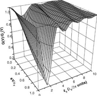
共20兲, for the contact as a function of the position of the defect 共0, z0兲in the limit of low voltage V→0. We observe a sup-pression of the conductance that is largest when the contact is placed directly above the defect and find that G is an oscillatory function of the defect position. In Fig. 4 we show the voltage dependence of the normalized conductance G共V兲/ Gc共V兲, Eq. 共20兲, for 0= 0 and as a function of the depth z0of the defect under the metal surface.
III. BALLISTIC CONTACT
In this section we consider another limit of a junction, a cylindrically symmetric, ballistic contact of adiabatic shape
共Fig. 5兲. The center of the contact is characterized by a ␦-function potential barrier of amplitude U. In one of the banks of the contact a single defect is situated at the point
r0=共0, z0兲, in the half-space z0⬎0, such that the distance ␥ between the center of the contact r = 0 and the defect is much larger than the characteristic length L of the con-striction共see Fig. 5兲. The shape of the contact is described by the radius as a function of the z coordinate a共z兲. The contact size is given by a共0兲= a0, while a共z兲→⬁ for 兩z兩→⬁. The adiabatic condition implies that the radius of the contact a共z兲 varies slowly on the scale of the Fermi wavelength. As a result, the electric potential V共r兲drops dominantly over the same characteristic length L, as can be derived from the con-dition of electroneutrality. In the Landauer formalism the ex-act distribution of V共r兲is not important for determining the conductance of a quantum constriction, which can be ex-pressed using only the difference of potentials V in the banks far from the contact. We will consider the effect of quantum interference on the conductance under conditions eV /FⰆ1
and kF␥共eV /F兲⬎1. Fluctuations of G共V兲 results from the
phase shift⌬that the wave function accumulates after be-FIG. 3. Dependence of the normalized conductance G / Gcfor a
single tunnel point contact as a function of the position of the defect 共0, z0兲; contact radius is a =F/ 4.
FIG. 4. Voltage dependence of the normalized conductance
G共V兲/ Gc共V兲of a tunnel point contact for0= 0 and as a function of the depth z0 of the defect under metal surface, contact radius is
a =F/ 4.
ing scattered by the defect and reflected by the contact,
⌬ ⬃共eV /F兲kF␥. If ␥ⰇL, the main part of the electron
trajectory is situated in the region where the local electric potential V共r兲 differs only little from its value V = 0 in the bank at z→⬁, and we neglect this small variation of the potential. Assuming hard wall boundary conditions, we need to solve the Schrödinger equation,
ⵜ2 ␣共,z兲+
2m*
ប2 关− g␦„r − r0…− U␦共z兲兴␣共,z兲= 0, 共23兲
with the boundary conditions
␣共兩兩= a共z兲;z兲= 0, 共24兲
and␣ represents the full set of quantum numbers.
In the adiabatic approximation15,16 the “fast” transverse and “slow” longitudinal variables in Eq. 共23兲 can be sepa-rated and the wave function takes on the form
␣共,z兲=⬜共,z兲共z兲, 共25兲 where=共m , n兲is a set of two discrete quantum numbers,17 which define the transverse local eigenvalues 共z兲 and eigenfunctions⬜共, z兲. The function⬜共, z兲depends on the coordinate z as a local parameter, and its derivatives with respect to z are small. Therefore Eq.共23兲 can be separated into two equations,
ⵜ2
⬜共兲= 2m*
ប2 共a兲, 共26兲
d2 dz2 +
2m*
ប2 关−共a兲兴= 0. 共27兲 The functions ⬜共兲and共z兲 satisfy the following con-ditions:
⬜共兩兩= a兲= 0, 共28兲
冏
d共z兲 dz冏
z0+0−
冏
d共z兲 dz冏
z0−0=2m *g
ប2 兩⬜共0兲兩 2
共z0兲, 共29兲
inc共z兲→eikz for z→−⬁, 共30兲
冏
d共z兲dz
冏
+0−
冏
d共z兲dz
冏
−0=2m *U
ប2 共0兲, 共31兲 where k =
冑
2m*/ប and inc共z兲 is the incident wave. Condi-tion共30兲means that we consider a waveinc共z兲of unit am-plitude, which moves from −⬁ toward the contact.For the subsequent calculations we make the explicit choice for the shape of the contact a共z兲= a0cosh共z / L兲. The condition of adiabaticity for this dependence a共z兲 is LⰇF. The solution of Eq.共26兲is given by
⬜共,,z兲=
1
冑
a共z兲Jm+1共␥mn兲Jm
冉
␥mn a共z兲冊
eim, 共32兲
having eigenvalues
= ប 2␥
mn
2
2m*a2共z兲, n = 0,1,2, . . . , m = 0, ± 1, ± 2, . . . . 共33兲
Here, we use cylindrical coordinates=共,, z兲 and␥mn is
the nth zero of Bessel function Jm. The energy spectrum共33兲
describes the quantized energy levels inside the constriction 共z⬍L兲and a quasicontinuous spectrum at zⰇL共the distance between the levels⌬→0 at兩z兩→⬁兲.
First, we consider a contact without an explicit barrier 共U = 0兲. A general solution for the longitudinal wave function 共z兲in Eq.共27兲has the form,
共z兲= A共1 −2兲−共ikL/2兲
⫻F
冉
− ikL − s,− ikL + s + 1,− ikL + s,1 − 2冊
+ B共1−2兲−共ikL/2兲
冉
1 − 2冊
ikL
F
冉
− s;s + 1,1 + ikL,1 − 2冊
,共34兲
where F共a , b , c ;兲 is the hypergeometric function, = tanh共z / L兲, and s =12共−1 + i
冑
共2L␥mn/ a0兲2− 1兲. Thecon-stants A and B can be found from the conditions 共29兲 and 共30兲. By using the asymptotic form of hypergeometric func-tion at z⬎z0ⰇL and in the limit of a small electron-impurity interaction constant m*gk
F/ប2Ⰶ1, we find
共z兲= t
冋
1 + gm*ikប2兩⬜共0;z0兲兩 2共1 + r
eikz0兲
册
eikz,共35兲
where rand tare the amplitudes of the reflected and trans-mitted waves far from the contact
r=⌫共− ikL − s兲⌫共− ikL + s + 1兲⌫共ikL兲
⌫共− s兲⌫共s + 1兲⌫共− ikL兲 , 共36兲
t=⌫共− ikL − s兲⌫共− ikL + s + 1兲
⌫共− ikL兲⌫共1 − ikL兲 . 共37兲 The expression for the current takes the form
I共V兲= e
冑
2m*兺
冕
zⰇLdS
冕
d冑
Im共␣*ⵜ
␣兲关nF共兲− nF共
+ eV兲兴. 共38兲
I共V兲=2e
h
冕
d兺
 T关nF共兲− nF共+ eV兲兴⫻
再
1 +gm *ប2k兩⬜共0兲兩 2兩r
兩cos共2kz0+兲
冎
. 共39兲 Here,T共兲= 1
1 + exp关2L共k− k兲兴, 共40兲
兩r共兲兩= 1
冑
exp关2L共k − k兲兴+ 1, 共41兲共兲=共k + k兲L兵1 − ln关共k + k兲L兴其−共k − k兲L
共
12兲
− 2kL共1− ln kL兲, 共42兲
k=
冑
2m*共0兲/ប is the quantized momentum of the transverse electron motion at the center of the contact,
共
12
兲
=⌫⬘
共
1 2兲
/⌫共
1
2
兲
⬇−1.96.The conductance G共V兲= dI / dV, in the low-temperature limit, is given by
G共V兲= G0
兺
T共F兲
⫻
再
1 + gm *ប2k
F
兩⬜共0兲兩2兩r兩cos共2k˜Fz0+兲
冎
, 共43兲 where G0= 2e2/ h is the quantum of conductance and k˜
F=
冑
kF2
+ 2meV /ប2. All energy-dependent functions are taken at=F. We also used the condition eV /FⰆ1.
The transmission coefficient is exponentially small T共兲⬃exp关−2L共k− k兲兴 for Ⰶ共0兲, while T共兲→1 above this energy,Ⰷ共0兲. For兩−共0兲兩Ⰶ共0兲, Eq.共40兲
agrees with the formula for the transmission coefficient that can be obtained in such a case for an arbitrary dependence a共z兲, by using an expansion near the point of minimum cross section, a共0兲 共see, e.g., Ref. 18兲. For very long constrictions 共L→⬁兲, Eq.共40兲transforms to a step function⌰共−共0兲兲. For large L the electrons are strongly reflected by the contact when k⯝k. Hence, for observation of conductance oscilla-tions in an adiabatic ballistic constriction the contact diam-eter should be chosen in such a way thatFⲏ共0兲, i.e., not very far from the middle of a conductance step.
In the case U⫽0 the boundary condition 共31兲 must be taken into account. At kⰇk, reflection due to the shape of the contact is negligibly small, as discussed above, and the conductance G共V兲 is also described by Eq.共43兲, but with
T共兲= 1
1 +共m*U/ប2k
⬘
兲2, 共44兲 兩r共兲兩= m*U/ប2k 
⬘
冑
1 +共m*U/ប2k⬘
兲2, 共45兲共兲= arcsin
冉
1
冑
1 +共m*U/ប2k⬘
兲2冊
, 共46兲
where k
⬘
=冑
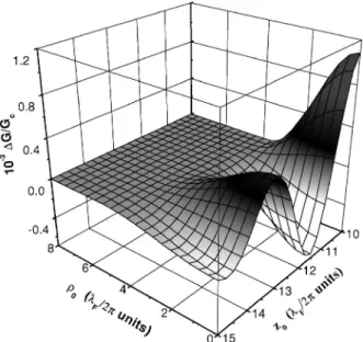
k2− k  2.Figure 6 shows the dependence of the oscillatory part of conductance⌬G共V兲= G共V兲− Gc共V兲, Eq.共43兲, on the position
of the defect at low voltage 共V→0兲 for a contact without barrier共U = 0兲. Here, Gc= G0兺T is the conductance in the
absence of a defect共g = 0兲. Figure 7 shows the dependence of the⌬G共V兲on applied bias voltage for a defect sitting on the axis of the contact共0= 0兲and as a function of the distance z0 from the contact center. In creating the plots of Figs. 6 and 7 we have used dimensionless parameter 2m*gk
F/ប2= 0.5,
2a0= 2.405F, and 2L = 10F, corresponding to a contact
having one allowed quantum conductance mode. FIG. 6. Dependence of the oscillatory part of normalized
con-ductance⌬G共0兲/ Gc共0兲of the ballistic point contact with the posi-tion coordinates of the defect共0, z0兲.
IV. DISCUSSION
The presence of an elastic scattering center located inside the bulk, either in the vicinity of a tunnel contact in an STM configuration or in one of the banks of a ballistic point con-tact, has been shown to cause oscillatory fluctuations in the conductance of the junction. For small contact radii 共aⰆF兲, these oscillations result solely from interference of
electron waves that are directly transmitted on the one hand, and electrons that are both backscattered by the defect and again reflected by the contact on the other. What now follows is a discussion as to whether this effect can be employed experimentally for three-dimensional mapping of subsurface impurities.
In the case of a tunnel contact, the oscillatory part of the conductance can be expressed by
Gosc共V兲
Gc ⬀
z02F2
␥4 sin 2k˜F␥, ˜kF␥Ⰷ1, 共47兲
where k˜F=
冑
kF2+ 2meV /ប2is the wave vector of electrons that are passing through the orifice, z0 is the depth of the defect under the surface, and␥is the distance between the contact and the defect. Comparing this to the results found for a ballistic contact, where
Gosc共V兲 Gc
⬀ F
2
a2共z0兲cos共2k ˜
Fz0+兲 共48兲 共hereis the phase the electron acquires after reflection by the contact兲, we see that although both oscillations have similar arguments, the expression for the ballistic case has an extra phase, which depends nonlinearly on the wave vec-tor k, making the signal hard to identify. Furthermore, the adiabatic condition, being an essential assumption in the bal-listic model, cannot be readily achieved experimentally.
Therefore, choosing the tunnel contact for experimental application seems most sensible. In that situation we can expect the information in the conductance signal about a defect’s whereabouts to be twofold: the amplitude will de-crease with growing distance␥, whereas the frequency of the oscillation is expected to increase upon enlarging the dis-tance from contact to defect. The actual experiment would consist of sensitively measuring共dI / dV兲共V兲curves on a tight grid of coordinates. The lateral positions of defects could
then be identified as the centers of radially symmetric pat-terns in this signal. Next, the depth of an impurity should be derived from the period of the oscillation in the共dI / dV兲共V兲 curve at0.
Assuming the numerical parameter 2m*gk
F/ប2= 0.5
in-troduced in Sec. III共which can be shown to be applicable for hard wall scatterers with atomic radius兲 and choosing the orifice to be located exactly above the defect 共␥= z0兲, the amplitude of the oscillation is expected to be 10−1Gc for
z0= 3 nm共with kF= 1010m−1兲.
Note that the chosen value of the interaction constant is rather large. We use such a value of the parameter to show the investigated effects more clearly in illustrations. For real values of parameter g⬇10−35erg cm3, which can be esti-mated from an electron effective scattering cross section ⬃1 Å2, the relative amplitude of oscillations is 10−2/ 10−3G
c.
Comparing this to previous STS experiments,19 where signal-to-noise ratios of 5⫻10−4 共at 1 nA, 400 Hz sample frequency兲have been achieved, we should be able to mea-sure defects located more than ten atomic layers under the surface.
As the period of the oscillation becomes longer for small z0, the minimum discernable depth will be determined by the maximum voltage that can be applied over the junction. For example, 30 mV is sufficient for probing a quarter of a con-ductance oscillation caused by a defect at 1 nm depth. The increase of the noise level inherent to measuring at elevated voltages will not pose a problem because the amplitude of the signal is much higher for small depths.
Finally, the anisotropy of the electronic structure will have to be taken into account. Materials with an almost spherical Fermi surface, such as Al or Au, realizing the condition of a free-electron gas, are expected to be most suitable. Further-more, deviations of spherical symmetry might be used as a secondary proof for the effectiveness of the method, i.e., in the case of Au共111兲, where the “necks” in the Fermi surface should cause a defect to be invisible when probed exactly from above.
This research was supported partly by the program “Nanosystems, nanomaterials, and nanotechnology” of Na-tional Academy of Sciences of Ukraine. Ye. S. A. wishes to acknowledge the INTAS grant for Young Scientists.
1Ph. Ebert, M. Heinrich, M. Simon, C. Domke, K. Urban, C. K. Shih, M. B. Webb, and M. G. Lagally, Phys. Rev. B 53, 4580 共1996兲.
2S. Heinze, R. Abt, S. Blügel, G. Gilarowski, and H. Niehus, Phys. Rev. Lett. 83, 4808共1999兲.
3M. Schmid, W. Hebenstreit, P. Varga, and S. Crampin, Phys. Rev. Lett. 76, 2298共1996兲.
4Hongbin Yu, C. S. Jiang, Ph. Ebert, and C. K. Shih, Appl. Phys. Lett. 81, 2005共2002兲.
5M. F. Crommie, C. P. Lutz, and D. M. Eigler, Nature共London兲
363, 524共1993兲; Science 262, 218共1993兲.
6S. Crampin, J. Phys.: Condens. Matter 6, L613共1994兲.
7C. Untiedt, G. Rubio Bollinger, S. Vieira, and N. Agraït, Phys. Rev. B 62, 9962共2000兲.
8B. Ludoph and J. M. van Ruitenbeek, Phys. Rev. B 61, 2273 共2000兲.
9A. Halbritter, Sz. Csonka, G. Mihály, O. I. Shklyarevskii, S. Speller, and H. van Kempen, Phys. Rev. B 69, 121411共2004兲. 10I. F. Itskovich and R. I. Shekhter, Fiz. Nizk. Temp. 11, 373
共1985兲 关Sov. J. Low Temp. Phys. 11, 202共1985兲兴.
12Ye. S. Avotina and Yu. A. Kolesnichenko, Fiz. Nizk. Temp. 30, 209共2004兲 关J. Low Temp. Phys. 30, 153共2004兲兴.
13Ye. S. Avotina, A. Namiranian, and Yu. A. Kolesnichenko, Phys. Rev. B 70, 075308共2004兲.
14I. O. Kulik, Yu. N. Mitsai, and A. N. Omelyanchouk, Zh. Eksp. Teor. Fiz. 63, 1051共1974兲.
15L. I. Glazman, G. B. Lesovik, D. E. Khmel’nitskii, and R. I. Shekhter, JETP Lett. 48, 238共1988兲.
16E. N. Bogachek, A. M. Zagoskin, and I. O. Kulik, Sov. J. Low Temp. Phys. 16, 796共1990兲.
17L. D. Landau and E. M. Lifshits, Quantum Mechanics共Pergamon, Oxford, 1977兲.
18E. N. Bogachek, A. G. Scherbakov, and Uzi Landman, Phys. Rev. B 54, R11094共1996兲.