POUR L'OBTENTION DU GRADE DE DOCTEUR ÈS SCIENCES
acceptée sur proposition du jury: Prof. H. Hofmann, président du jury
Prof. P. Muralt, directeur de thèse Prof. I. Katardjiev, rapporteur
Dr T. Metzger, rapporteur Prof. P. Ryser, rapporteur
High Coupling Materials for Thin Film Bulk Acoustic
Wave Resonators
THÈSE N
O4489 (2009)
ÉCOLE POLYTECHNIQUE FÉDÉRALE DE LAUSANNE
PRÉSENTÉE LE 18 SEPTEMBRE 2009À LA FACULTÉ SCIENCES ET TECHNIQUES DE L'INGÉNIEUR LABORATOIRE DE CÉRAMIQUE
PROGRAMME DOCTORAL EN SCIENCE ET GÉNIE DES MATÉRIAUX
Suisse 2009 PAR
i
Abstract
Radio frequency (RF) filters based on bulk acoustic wave resonances in piezoelectric thin films have become indispensable components in mobile communications. The currently used material, AlN, exhibits many excellent properties for this purpose. However, its bandwidth is often a limiting factor. In addition, no tuning is possible with AlN. Ferroelectrics would offer both larger coupling to achieve larger bandwidths, and tunability. However, their acoustic properties are not well known, especially in the thin film case. The goal of this thesis is to investigate the potential and identify the limitations of ferroelectric thin films for thickness mode resonators in the 0.5 - 2 GHz range.
The Pb(Zrx,Ti1−x)O3 (PZT) solid solution system is the main candidate, since it is known for
its large piezoelectric constants and its growth is already well studied. As a main test vehi-cle, free standing thin film bulk acoustic resonator (TFBAR) structures with Pt/PZT/Pt/SiO2
membranes were successfully fabricated using silicon micro-machining techniques. The main drawback of ferroelectrics is the damping of acoustic waves by domain wall motion both in the RF electric field and in the pressure wave. For this reason films with varying orientations and compositions were investigated. From the device structures the electro-mechanical coupling con-stants kt2, the quality factors (Q-factors) and several materials parameters have been obtained. High coupling constants have been found for sol-gel Pb(Zr0.53,Ti0.47)O3 films with a{100}
tex-ture, kt2 is found to be 0.4 for a 1μm thick film and 0.8 for a 3.8 μm thick film. However, the
Q-factors of these films are low, 18 for the first film and 3 for the second film. The increase of
kt2 and the decrease of the Q-factor with frequency indicates that the domains present in these films contribute to these characteristic parameters. It was generally observed that high coupling constant are associated to low Q-factors. This became evident when comparing films with 53/47 composition, where both tetragonal and rhombohedral phases are present, to tetragonal films as well as when comparing {100}textures with (111) textures. Both for the 53/47 composition and for the {100} texture, ferroelastic domain walls are thought to play a bigger role than for tetragonal compositions and (111) textures. The highest figure of merit (FOM) of about 15 was found when combining the composition leading to a high coupling constant (53/47) and the orientation leading to lower losses (111). However the losses even in this film are too high for RF-filter applications. On the other hand, films with low Q-factors but high coupling could prove very useful as transducers for ultrasonic imaging applications, where low Q-factors are desired.
The stiffness coefficients of the studied PZT films were shown to be higher than expected from ceramics data. Most likely the stiffness of ceramics always contains domain contributions leading to softening. In contrast, in textured films the variety of domain orientation is very much reduced.
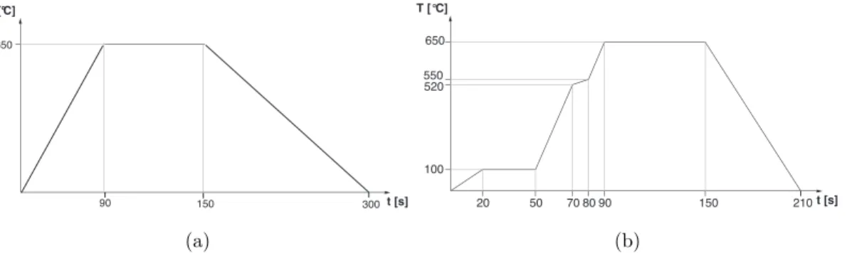
In order to reduce losses due the presence of ferroelastic domains three different potential so-lutions were explored. The first idea was to manipulate the domain populations of the films deposited on silicon by using heat and vacuum treatments. Silicon substrates are known from
previous works to be unfavourable for high c-domain fractions. It was discovered that an an-neal in vacuum at 550◦C lead to a significant reduction of c-domains in tetragonal 30/70 PZT ({100}). On the contrary, if the sample was subjected to a compressive stress during cooling, the
c-domain fraction could be increased. Analysis of the film stress versus temperature curves re-vealed a trend consistent with theoretical predictions, i.e. a phase boundary between thec/a/c/a
and thea1/a2/a1/a2domain patterns between room temperature and the Curie temperatureθC.
However, even though this method reveals interesting results, it can not be exploited as a method to achieve a sufficient c-domain population.
The second idea explored was the implementation of a high thermal expansion material as a substrate. PZT films deposited on MgO are known to be compressive due to the difference in thermal expansion of the two materials. The compressive stress leads to highly c-axis oriented PZT films. Devices using MgO substrates were fabricated, however difficulties in the micro-machining of the MgO substrate inhibited a complete liberation of the membrane. Nevertheless, preliminary measurements indicate these devices could lead to both high coupling and high Q-factors, suggesting that further detailed study of this method is worthwhile.
As a third method for avoiding ferroelastic domains, the uniaxial ferroelectric potassium lithium niobate (KLN) was explored. The unique ferroelectric axis in this material means that only 180◦ domain walls are present, which can theoretically be removed by poling. This material has been deposited in thin film form using pulsed laser deposition (PLD). KLN thin films with a {001} texture were deposited successfully on Pt/Si substrates. The films were piezoelectric with ad33,f
value of around 10 pm/V and a dielectric constant of 250. This is the first time that piezoelectric properties were measured on KLN thin films. A columnar structure has been observed, however the small grain size and the rough surface currently make it difficult to apply this material to TFBAR’s.
iii
Zusammenfassung
Radiofrequenz-Bandpassfilter basierend auf akustischen Raumwellen-D¨unnschichtresonatoren (TFBAR) sind zu unentbehrlichen Komponenten f¨ur mobile Telekommunikation geworden. Das gegenw¨artig eingesetzte Material AlN besitzt zwar viele hervorragende Eigenschaften f¨ur diese Anwendung; es ist jedoch bez¨uglich seiner Bandbreite limitiert. Ausserdem ist Tuning bei AlN nicht m¨oglich. Ferroelektrika w¨urden sowohl hohe Kopplungskonstanten, die zu breiten Bandbrei-ten f¨uhren, bieten, als auch ein Tuning erm¨oglichen. Allerdings sind die akustischen Eigenschaften von ferroelektrischen Materialien, vor allem im Fall von d¨unnen Schichten, noch weitgehend un-bekannt. Das Ziel dieser Dissertation ist, das Potential und die Grenzen von ferroelektrischen D¨unnschichten in Resonatoren basierend auf Dickenschwingungen im Frequenzbereich von 0.5 -2 GHz zu untersuchen.
Das Pb(Zrx,Ti1−x)O3 (PZT) Mischkristallsystem ist ein vielversprechender Kandidat, da es f¨ur
seine hohen piezoelektrischen Konstanten bekannt ist und die Herstellung von PZT Schichten gut beherrscht wird. Freistehende Pt/PZT/Pt/SiO2Membrane wurden mittels Silizium Mikrofabri-kationstechniken hergestellt und als Testruktur benutzt. Der gr¨osste Nachteil von Ferroelektrika ist die D¨ampfung der akustischen Wellen durch Bewegungen der Dom¨anenw¨ande im elektrischen Feld und in der Druckwelle. Aus diesem Grund wurden Schichten mit unterschiedlichen Orien-tierungen und Zusammensetzungen studiert. Impedanzmessungen der Resonatoren erm¨oglichen die Bestimmung der Kopplungsfaktoren (kt2), Qualit¨atsfaktoren (Q-Faktor) und mehrerer Mate-rialskonstanten. Grosse Kopplungsfaktoren wurden f¨ur Pb(Zr0.53,Ti0.47)O3Sol-Gel Schichten mit
einer {100}Textur erzielt, ein Kopplungfaktor von 0.4 ist f¨ur eine 1μm dicke Schicht ermittelt worden und 0.8 f¨ur eine 3.8 μm dicke Schicht. Allerdings sind die Q-Faktoren dieser Schichten klein, 18 f¨ur die erste Schicht und 3 f¨ur die zweite. Der Anstieg von kt2 und die Abnahme des Q-Faktors mit steigender Frequenz deuten an, dass die Dom¨anen, die in diesen Schichten vorhan-den sind, zu diesen Werten beitragen. Hohe Kopplungskonstanten konnten in allen hergestellten Schichten mit kleinen Q-Faktoren assoziiert werden. Dies wurde beim Vergleichen von 53/47 Schichten (bestehend aus rhombohedrischer und tetragonaler Phase) mit tetragonalen Schich-ten, als auch beim Vergleichen von {100}Texturen mit (111) Texturen beobachtet. Sowohl bei Schichten mit 53/47 Zusammensetzung als auch bei {100}texturierten Schichten spielen ferro-elastische Dom¨anenw¨ande eine gr¨ossere Rolle als bei tetragonalen Zusammensetzungen und bei (111) texturierten Schichten. Der gr¨osste G¨utefaktor von ungef¨ahr 15 wurde beim Kombinieren von einer Zusammensetzung, die zu hoher Kopplung f¨uhrt (53/47), mit einer Textur, die zu tiefen Verlusten f¨uhrt (111), erreicht. Trotzdem sind die D¨ampfungsverluste zu hoch f¨ur eine Anwen-dung in RF-Filtern. Kleine Q-Faktoren kombiniert mit hohen Kopplungskonstanten sind aber f¨ur eine andere Anwendung interessant, n¨amlich im Bereich der medizinischen Ultraschallabbildung, wo kleine Q-Faktoren erw¨unscht sind und immer h¨ohere Frequenzen interessant werden.
Um die D¨ampfungsverluste verursacht durch ferroelastische Dom¨anen zu mindern, wurden drei potenzielle L¨osungen untersucht. Die erste Idee war, die Dom¨anenpopulation von auf Silizium
aufgebrachten Schichten mit Hilfe von W¨armebehandlungen in Vakuum zu beeinflussen. Es ist bekannt, dass Silizium als Substrat unvorteilhaft ist um einen hohen Anteil an c-Dom¨anen zu erreichen. Es wurde beobachtet, dass eine W¨armebehandlung im Vakuum bei 550◦C bei te-tragonalen (30/70) ({100}) zu einer Abnahme des c-Dom¨anen Anteils f¨uhrte. Wurde hingegen w¨ahrend der W¨armebehandlung zus¨atlich ein kompressiver Druck auf die Schicht ausge¨ubt, konn-te derc-Dom¨anen Anteil leicht erh¨oht werden. Bei der Analyse der Spannungs-Temperatur Kur-ven wurde ein theoretisch vorausgesagtes Verhalten beobachtet, n¨amlich der Phasen¨ubergang von c/a/c/a zua1/a2/a1/a2 Dom¨anenkonfigurationen. Dieser Phasen¨ubergang wurde zum
ers-ten Mal experimentell beobachtet. Obwohl Ver¨anderungungen der Dom¨anenkonfigurationen mit W¨armebehandlungen im Vakuum beobachtet werden k¨onnen, ist dies keine geeignete Methode, einen gen¨ugend grossenc-Dom¨anen Anteil zu erhalten.
Der zweite Ansatz, der erforscht wurde, ist die Anwendung von einem Substrat mit einem hohen thermischen Ausdehnungskoeffizient. Auf MgO gewachsene PZT Schichten sind kompressiv, da der thermische Ausdehnungskoeffizient von MgO gr¨osser ist als der von PZT. Die Druckspan-nung f¨uhrt zu Schichten mit derc-Achse senkrecht zur Substratebene. PZT Schichten mit (001) Orientierung wurden auf MgO Substraten erfolgreich aufgebracht, die Herstellung von Membra-nen auf diesem Substrat war jedoch schwierig. Die Methode ist vielverprechend, eine geeignete
¨
Atztechnik f¨ur Resonatoren auf MgO Substraten muss jedoch noch erarbeitet werden.
Als dritte Methode, um ferroelastische Dom¨anen zu vermeiden, wurde das uniaxiale Ferroelek-trikum Kaliumlithiumniobat (KLN) in Betracht gezogen. Da nur eine ferroelektrische Achse in diesem Material existiert, k¨onnen theorethisch alle Dom¨anen durch Polen entfernt werden. KLN wurde mit Laserstrahlverdampfen (pulsed laser deposition (PLD)) auf Pt/Si Substraten aufgebracht. Die Filme sind piezoelektrisch mit einem piezoelektrischen Koeffizienten d33,f von
ungef¨ahr 10 pm/V und einer Dielektrizit¨atskonstante von 250. Piezoelektrische Eigenschaften von KLN D¨unnschichten wurden zum ersten Mal gemessen. Die rauhe Oberfl¨ache und die schwer kontrollierbare Zusammensetzung zeigen aber, dass die Studien dieser Schichten noch im An-fangsstadium sind, aber eine Anwendung in TFBAR’s nicht auszuschliessen ist.
Stichw¨orter: Ferroelektrika, akustischer Raumwellen-D¨unnschichtresonator, TFBAR, PZT,
Contents
Contents vii
1 Introduction 1
1.1 BAW resonators: Introduction and Applications . . . 1
1.1.1 Acoustic waves in solids . . . 1
1.1.2 Piezoelectricity . . . 3
1.1.3 Bulk acoustic wave resonators . . . 5
1.1.4 Types of bulk acoustic wave resonators . . . 6
1.1.5 Bulk acoustic wave resonator applications . . . 7
1.2 Materials used for thin film BAW devices . . . 9
1.2.1 Material considerations for the piezoelectric layer . . . 9
1.2.2 AlN and ZnO . . . 11
1.2.3 PZT solid solution system . . . 11
1.3 State of the art of PZT in BAW resonators . . . 14
1.4 PZT Materials Losses and Domain Considerations . . . 17
1.4.1 PZT Materials Losses . . . 17
1.4.2 Ferroelectric Domains and their Contribution to Losses . . . 20
1.5 Thesis aims and approach . . . 24
1.6 Thesis outline . . . 25
2 PZT thin films: Synthesis and Properties 27 2.1 PZT deposition methods . . . 28
2.2.1 Platinum bottom electrode . . . 35
2.2.2 Orientation control for (111) preferred orientation . . . 36
2.2.3 Orientation control for{100} preferred orientation . . . 38
2.3 Domain considerations in tetragonal PZT films . . . 40
2.3.1 (111) textured tetragonal PZT films . . . 40
2.3.2 {100}textured tetragonal PZT films . . . 41
2.4 Dielectric characterisation . . . 55
2.4.1 Field dependence of the dielectric constant . . . 57
2.4.2 Frequency dependence of the dielectric constant . . . 60
2.5 Piezoelectric characterisation . . . 63
2.6 Summary . . . 65
3 TFBAR Fabrication and Characterisation 69 3.1 Resonator design and fabrication steps . . . 69
3.1.1 Design . . . 69
3.1.2 Process flow . . . 70
3.2 Resonator measurement and modelling . . . 75
3.3 Numerical model simulation results . . . 77
3.4 Field dependence of TFBAR characteristics . . . 89
3.5 Discussion of derived materials parameters . . . 92
3.6 Summary . . . 95
4 Alternative materials and routes 99 4.1 KLN . . . 99
4.1.1 KLN structure and properties . . . 100
4.1.2 Literature review of KLN thin film synthesis . . . 102
4.1.3 KLN thin film deposition by PLD . . . 103
4.1.4 KLN thin film characterisation . . . 104
4.1.5 Summary . . . 109
4.2 PZT on MgO . . . 110
4.2.1 Growth issues . . . 110
4.2.2 TFBAR fabrication . . . 111
4.2.3 PZT and TFBAR characterisation . . . 112
4.2.4 Summary . . . 113
5 Conclusions and Outlook 121 5.1 Conclusions . . . 121
5.2 Outlook . . . 124
A List of Symbols and their Units 127 B List of abbreviations 129 C Simulation of stress-temperature curves 131
List of Tables 135
List of Figures 136
Bibliography 145
Chapter 1
Introduction
This Chapter starts with an introduction to bulk acoustic wave (BAW) resonators begin-ning by introducing acoustic waves in solids, explaibegin-ning the operation principle of BAW resonators and illustrating a few applications. The principal materials in use or consid-ered to be used for BAW applications are discussed next. The following section gives an overview of the state of the art of PZT in BAW resonators, PZT being the main material considered for high coupling BAW applications. Alternative materials and methods shall be introduced in Chapter 4. Since the main problem of PZT for BAW applications are the acoustic losses in the material, Section 1.4 is devoted to this subject. Finally the aims of this thesis will be described followed by an outline of the thesis.
1.1
BAW resonators: Introduction and Applications
1.1.1
Acoustic waves in solids
Just as we can only see a tiny part of the frequency range of the electromagnetic spectrum, human hearing is only a small fraction of the frequency range of the full acoustic wave spectrum. In each case the full spectrum can be described by one theory, the theory of electromagnetic waves for optics and the theory of stress waves in material media for acoustics.
Sound waves propagate in a variety of media, including gas, liquids, and solids. In solid materials there a two basic types of acoustic waves. One type is a longitudinal wave (see Figure 1.1a), in which the displacement is parallel to the wave vector. The velocity depends on the material, but is typically between 5000 to 10 000 m/s. The second basic
wave type is the transverse (shear) wave, in which the displacement is normal to the wave vector (see Figure 1.1b). These waves generally have a lower velocity of typically 3000 to 6000 m/s. Waves can also propagate with a combined longitudinal and shear motion. The waves discussed up to now are called bulk acoustic waves (BAW’s), meaning they can propagate freely in the bulk, as if in an infinite medium.
If the propagation medium is bounded, acoustic waves are mainly governed by the bound-ary conditions. When the wavelength is no longer much smaller than the dimensions of the medium, the boundary conditions define the propagating waves. The most common boundary conditions are surfaces and plates. A summary of some important wave types possible in solids is shown in Table 1.1.
Medium Acoustic Wave Types Displacement in Solids
Bulk Longitudinal wave Parallel to wave direction
Bulk Transverse (Shear) wave Perpendicular to wave direction
Surface Rayleigh wave Elliptical orbit close to surface in x-z plane
Plate Lamb Wave Elliptical orbit in x-z plane symmetrically
or anti-symmetrically throughout plate thickness Table 1.1: Wave types and their characteristic particle displacement.
One wave of great interest for electronics is the surface acoustic wave (SAW). The wave is guided along the surface, with its amplitude decaying exponentially with depth. Dis-placements result from both longitudinal and transverse motion to create an elliptic orbit. These waves are exploited to make SAW filters and also for surface inspection in ultra-sonic imaging. This wave type was first proposed by Rayleigh to explain wave propagation during earthquakes.
Lamb waves can only be generated in structures a few wavelengths thick. As with surface acoustic waves, Lamb waves are a combination of longitudinal and transverse waves. There are two families of lamb waves, symmetric lamb waves have a symmetry plane in the middle of the plate and anti-symmetric lamb waves where both the top and bottom surface of the plate move in the same direction (see Figure 1.2). The velocity of these waves depends on the relationship of wavelength to plate thickness.
1.1. BAW RESONATORS: INTRODUCTION AND APPLICATIONS 3 λ Propagation direction (a) λ Propagation direction (b)
Figure 1.1: Schematic of acoustic waves in an infinite solid (a) longitudinal mode (b) transverse (shear) mode. Dots represent particles at rest and lines indicate instantaneous position when a wave is present. After Weigel [1].
Propagation direction
(a)
Propagation direction
(b)
Figure 1.2: Schematic of lamb waves in a plate (a) symmetric lamb wave (b) anti - symmetric lamb wave. Dots represent particles at rest and lines indicate instantaneous position when a wave is present.
1.1.2
Piezoelectricity
In most of the applications, piezoelectric materials are used to generate and detect acoustic waves. The lattice of a piezoelectric material is characterised by the absence of an inversion symmetry. Applying an electric field to this materials changes the mechanical dimensions. Conversely, applying a mechanical constraint an electrical field is generated.
In a piezoelectric the elastic and electrical parameters are coupled in a bilinear term. If the electric field Ei, stressTij and temperature θ are taken as independent variables the appropriate thermodynamic potential is the Gibbs free energy Gof a dielectric:
where U is the internal energy of the system, σ the entropy, Sij the strain and Di the dielectric displacement. The differential free energy dGreads as:
dG=−σdθ−SijdTij−DidEi (1.2)
For small enough variablesTijandEi, the integral form can be expressed in bilinear terms as: ˜ G=−1 2s E ijklTklTij− 1 2ε T ijEiEj−dijkTklEi (1.3) when dθ = 0. From this relation the dielectric, elastic and thermal equations of state can be written and from their differential form the compliances are obtained [2, 3]. The compliance coefficients relate different fields with each other, the most important ones are defined as the elastic compliance relating stress to strain, the permittivity relating displace-ment to electric field, piezoelectric constants relating stress/strain to displacedisplace-ment/electric field, pyroelectric constants relating displacement to temperature and thermal expansion coefficients relating strain to temperature [2]. With these definitions and with the more practical case of the temperature being constant the adiabatic piezoelectric equations can be derived: Sij =− ∂G˜ ∂Tij =sEijklTkl+dkijEk (1.4) Di=− ∂G˜ ∂Ei =dijkTjk+εTijEj (1.5)
with the compliance coefficients as described above: the elastic compliancesijkl, the piezo-electric constantdijkand the permittivity or dielectric constantεij. It is important to note that the boundary conditions play a crucial role in the resulting response of the material, the difference of the dielectric permittivity at constant stress or constant strain can be considerable. The same applies for the electrical boundary conditions (electric field or displacement constant). It is often useful to use the strain S as independent variable. This leads to the following equations of state:
Tij =cEijklSkl+ekijEk (1.6)
Di=eEijkSjk+εTijEj (1.7)
1.1. BAW RESONATORS: INTRODUCTION AND APPLICATIONS 5
1.1.3
Bulk acoustic wave resonators
Since the velocity of acoustic waves in solids is small as compared to electromagnetic waves, resonators based on acoustic standing waves with very small sizes can be built. The thickness mode resonance of BAW in a thin uniform plate of thickness t is given when:
f = N·v
2t N ∈ {1,3,5...} (1.8)
withf the resonance frequency,v the wave velocity. Waves can be generated by applying a voltage on the piezoelectric material. The construction principle of such a resonator is shown in Figure 1.3. What is needed is an acoustically isolated piezoelectric layer (piezolayer) with a top and bottom electrode. The piezoelectric tensor of the piezolayer has to be suitably oriented with respect to the electrodes. A longitudinal acoustic wave can be generated in a piezolayer with the piezoelectric coefficient d33 perpendicular to the electrodes by applying a AC voltage. If the frequency is chosen correctly the layer will resonate between the two electrodes. The contour mode wave that could also be excited in the piezoelectric cannot follow at the frequencies of resonance for the thickness mode, since the thickness, t, is a lot smaller than the width, a, of the resonator. This means that the film can be assumed to be clamped in x and y directions, and free to move in z
direction. λ/2 VAC t a t << a x y z
Figure 1.3: Schematic of a bulk acoustic resonance in a piezoelectric plate. The vertical dimen-sion is exaggerated for the sake of clarity. The pressure amplitude for the fundamental mode is sketched in the vibrating part of the device.
Longitudinal sound waves in solids typically amount to 5’000 to 10’000 m/s. Evaluating Equation 1.8 for a practical thin film thickness of 0.1 to 5μm, resonance frequencies in the range of 0.5 to 50 GHz are calculated. This covers the interesting range of 0.5 to 15 GHz in which ultrasonic resonators are superior to digital and pure electromagnetic solutions.
1.1.4
Types of bulk acoustic wave resonators
There are different approaches to obtain an acoustically isolated piezolayer. Figure 1.4 shows three possible device configurations based on thin films as the piezoelectric material. The first approach is a membrane structure supported at the edge by the substrate. The fabrication steps involve deposition of the piezoelectric film on a supporting substrate and removal of a portion of the substrate to create membranes. Since the acoustic impedance (defined as ZA = ρ·v where ρ is the density and v the sound velocity) of air is a lot lower than of a solid, most of the energy is reflected at the air/solid boundary. Another approach, also using air to reflect the acoustic wave, is to micromachine the surface. By depositing a sacrificial layer before deposition of the piezolayer with its electrodes and removing this layer as the last step, an air gap under the resonator can be created. A quite different approach is the SMR (solidly mounted resonator) since the resonator is fixed to another solid. The acoustic isolation can be achieved by using an acoustic mirror. The acoustic mirror is made by alternating quarter wavelength thick films of a high and a low acoustic impedance. At each boundary between the high and low impedance layers a large percentage of the wave will be reflected and will sum up to the correct phase due to the λ/4 thickness of the layers. The result is a practically isolated acoustic resonator in a certain wavelength interval around λ.
Piezoelectric Piezoelectric Piezoelectric Electrodes Electrodes Electrodes
Substrate etched via back side
Substrate Substrate Air Gap a) b) c) Reflector Stack
}
Figure 1.4: Configurations for thin film resonators. (a) Membrane formed by etching from the back side of the substrate. (b) Resonator isolated by an air gap. (c) Solidly mounted resonator using an acoustic reflector stack.
1.1. BAW RESONATORS: INTRODUCTION AND APPLICATIONS 7
1.1.5
Bulk acoustic wave resonator applications
Thin film bulk acoustic wave resonators (TFBARs) are combined in order to fabricate BAW-filters. TFBARs can be used in filter design as bandpass filters or image rejection filters (narrow passband with signal rejection at adjacent lower frequencies). Passband filters may be realised with electrically coupled TFBARs using a ladder or lattice topology or may also apply acoustically coupled resonators which are stacked on top of each other. As an example, the construction principle of a ladder filter is shown in Figure 1.5 and its working principle in Figure 1.6. In ladder filters two groups of resonators are used, series resonators and shunt resonators. The series resonators are the resonators connected in series in the circuit diagram. All the series resonators have the same resonance frequency
fs,series and the all the shunt resonators have a resonance frequencyfs,shunt, shifted down by adding an additional layer on these resonators. In the center of the passband the series resonators are at minimum impedance and thus let the signals pass, whereas the shunt resonators are at maximum impedance and thus will not shunt the signal.
Figure 1.5: Topology of 312-stage ladder filter (After Aigner [6]).
Another way of realising bandpass filters is by lateral acoustic coupling of thickness- or shear-mode resonance. Grudkowski et al.[4] demonstrated in 1980 the laterally coupled, thin film Monolithic Crystal Filter (MCF) with 8.5 dB insertion loss and 40 dB rejection. Bandpass filters can also be realised by stacking two resonators which couple acoustically in the thickness mode. A large out-of-band rejection is achieved because of the grounded middle electrode. Lakin et al.[5] introduced the thin film Stacked Crystal Filter (SCF) in 1986, as well as the electrically coupled ladder filter.
The characteristics of these filters (see Figure 1.7) are highly dependent on the properties of the piezoelectric layer. While some parameters are a matter of design, insertion loss
Figure 1.6: Working principle of a ladder filter (After Aigner [6]).
and bandwidth are ultimately defined by the acoustic and piezoelectric properties of the piezolayer. Depending on the application the demands on the filter characteristics differ. The main applications of RF-filters are mobile phones (400 MHz to 2.2 GHz), global positioning systems (GPS, 1.575 GHz), WLAN (Wireless Local Area Network) and short range systems such as Bluetooth and cordless phones [6]. The main types of RF-filters are ceramic filters, SAW and BAW filters. Since wireless systems continue to be miniaturised, the requirements on these filters increase. SAW technology provides high performance filters, avoiding the too large ceramic (dielectric) filters, but the tendency to go to higher frequencies is pushing this technology to its limits. Figure 1.8 shows the frequency range where BAW technology is interesting. BAW technology is needed at high frequencies where a small size and high performance are required. The performance of a filter can be judged by its power handling capabilities, size, the steepness of the filter skirts and insertion loss.
1.2. MATERIALS USED FOR THIN FILM BAW DEVICES 9
High coupling materials are needed for applications where a large bandwidth is demanded. Materials used currently as the piezoelectric in BAW resonators and materials being con-sidered for future use shall be discussed in the following section.
Pass band f S21 0 dB -3 dB -40 dB Insertion loss f1 fcenter f2 relative bandwidth = (f2-f1) / fcenter Stop band 1 Stop band 2 Rejection [dB] [dB]
Figure 1.7: Schematic showing the main characteristic of a RF-frequency filter (After Aigner [7]).
SAW LC circuits frequency [GHz] Ceramic filters BAW 1 3 5 performance
Figure 1.8: RF frequency range vs. performance of RF filters showing the frequency range where BAW technology is of interest (After Aigner [7]).
1.2
Materials used for thin film BAW devices
1.2.1
Material considerations for the piezoelectric layer
Ideally, the piezoelectric layer for thin film resonators should be a high quality single crys-tal, having a single orientation. On most substrates suitable for device microfabrication the deposited films are polycrystalline. Nonetheless high quality textured thin films with
a columnar structure can be made to meet the requirements on TFBARs for telecommu-nication applications. The materials parameters of the piezoelectric layer that need to be considered for TFBAR applications shall be briefly described.
Piezoelectric coupling coefficient kt2
The piezoelectric coupling coefficient for thickness extensional modek2t is a dimensionless measure of electromechanical energy conversion efficiency of this mode. It is determined by the piezoelectric, elastic and dielectric constants as:
kt2= e 2 33 cD 33εS33 (1.9) where e33 is the piezoelectric constant, cD33 is the elastic stiffness at constant electric dis-placement and εS
33 is the clamped dielectric permittivity. The conversion efficiency is naturally bounded to 0 ≤ kt2 < 1. The coupling factor is important since it defines the maximum achievable bandwidth.
Acoustic velocity vD
The acoustic velocity (or sound velocity) of the longitudinal mode along the polar axis 3 is given by vD= cD33 ρ (1.10)
and defines the resonance frequency of a slab cut perpendicular to the polar axis 3 (ac-cording to Equation 1.8). The velocity depends primarily on the elastic stiffness cD
33 and the mass density ρ of the material and to a lesser extent on the piezoelectric properties of the medium through the piezoelectric contribution to the elastic stiffness [8]:
cD33=cE33+e 2 33 εS 33 (1.11) or cE33 =cD33·(1−k2t) Acoustic loss
The material limited losses in acoustic materials can be expressed by the motional time constant [9]:
τ1= η
cD 33
(1.12) which is dependent on the acoustic viscosity η and the elastic stiffness of the film. This quantity can also be seen as the imaginary part of the elastic constants proportional to the viscosity:
1.2. MATERIALS USED FOR THIN FILM BAW DEVICES 11
The mechanical quality factor of the piezoelectric layer can then be written as:
Q= 1 tanγ =
1
ωτ1 (1.14)
A high quality factor (Q-factor) is needed in order to limit damping of the wave. The effective Q-factor of a resonator also depends on other features of the device, such as resistive losses in electrodes.
Dielectric constant εr
The impedance level of a resonator is determined by the resonator size, the thickness of the piezolayer and the dielectric constant. A high dielectric constant allows for reduction of the resonator size at a given frequency. The dielectric constant inzdirection of a clamped film is denoted ε33.f.
Attractive materials for TFBARs exhibit high Q-factors and for RF applications in addi-tion a high kt2.
1.2.2
AlN and ZnO
Both AlN and ZnO have a wurtzite structure and show a longitudinal piezoelectric response along the [0001] direction. To obtain good piezoelectric coefficients columnar grains with a (0001) texture with the same polar direction are needed. High quality films can be pro-duced by reactive magnetron sputtering. Relevant properties of AlN and ZnO are shown in Table 1.2, together with PZT for comparison. Both AlN and ZnO meet the material property requirements to produce RF-filters for mobile communications. However AlN has some advantages. One important advantage is its compatibility with silicon semiconductor technology, whereas ZnO is more problematic. AlN has lower dielectric losses and higher thermal conductivity, which means it can handle higher power levels, whereas ZnO has high dielectric losses and tends to have a low resistivity [9, 10]. In conclusion TFBARs based on AlN meet the specifications needed for mobile communications and so far ZnO has not been demonstrated as a feasible alternative.
1.2.3
PZT solid solution system
The lead zirconate titanate system is commonly used in resonators, but as a ceramic ma-terial at low frequencies for example for medical applications at 3 to 10 MHz. PZT in thin film form has found applications in sensors and actuators due to its high piezoelectric constants. Resonators based on PZT thin films have not been commercialised yet. Pb(Zrx,
Coefficients ZnO AlN PZT
Longitudinal sound velocityvD 6350 11000 4000...6000 along direction 3 [m/s]
Dielectric constantεS
33 10.9 10.5 200...1300
Dielectric losses tanδ 0.01...0.1 0.003 0.01...0.03
Piezoelectric constant d33,f [pm/V] 5.9 3.9...5.1 60...130 StiffnesscD
33 [GPa] 208 395 90...160
Acoustic losses low low high
Table 1.2: Comparison of piezoelectric materials for TFBARs. Values from references [6, 10, 11].
Ti1−x)O3 is a solid solution of lead titanate (PbTiO3) and lead zirconate (PbZrO3) with a perovskite structure. At room temperature, the system Pb(Zrx, Ti1−x)O3 is tetragonal for x = 0-0.53 and rhombohedral when x > 0.53 [3, 12]. In the tetragonal case the ferro-electric polarisation points along the 001 direction, in the rhombohedral case it points along the 111 direction. A schematic of the tetragonal perovskite structure is shown in Figure 1.10. The lead zirconate titanate ( PbZrO3 - PbTiO3) phase diagram is shown in Figure 1.9 [13]. The narrow region where these two symmetries meet, at a Ti/Zr ratio of 53/47, is called the morphotropic phase boundary (MPB). At or near this boundary, many properties peak: the piezoelectric coefficients, the coupling coefficient and the rela-tive permittivity. The high values of these parameters are exploited in many applications such as sensors, transducers and applications in the field of microelectromechanical sys-tems (MEMS). These high values of piezoelectric coefficients at the morphotropic phase boundary are due to the presence of both rhombohedral and tetragonal phases, which enhances the possibilities of polarisation orientation. Or, according to newer theory, the existence of a monoclinic phase in which the polarisation can be rotated with almost no anisotropy in the {110} plane [14]. PZT thin films with a tetragonal composition are one of the main candidates for non-volatile memory applications due to their large remanent polarisation.
The properties of PZT thin films are sensitive both to the composition of the system and to the crystallographic orientation of the film. This means that films can be tailored to suit the requirements of a certain application. However as will be shown in the following Chapters these properties are correlated and cannot be adapted independently. In practice this means that certain compromises need to be made when choosing the composition and orientation of the PZT film.
co-1.2. MATERIALS USED FOR THIN FILM BAW DEVICES 13
Figure 1.9: Phase diagram of the Pb(Zrx, Ti1−x)O3 solid solution. The morphotropic phase
boundary separates the tetragonal and rhombohedral ferroelectric phases. The subscripts A and F stand for antiferroelectric and ferroelectric phases, the letters C, T, R and O stand for cubic, tetragonal, rhombohedral and orthorombic phases. After Jaffe [13].
Pb2+ O 2-Zr4+, Ti4+
Figure 1.10: Schematic of the tetragonal PZT unit cell with a perovskite structure. Semitrans-parent circles indicate equilibrium position of the cubic perovskite structure. The displacement of the centre ion and the surrounding oxygen ions creates a dipole.
efficients, leading to larger bandwidth, lower sound velocity, which means thinner films for a given frequency and higher dielectric constants, reducing resonator areas. PZT is of interest for BAW resonator applications with frequencies around 1-2 GHz, since these frequencies require very thick films for materials such as AlN. In addition tailoring of its properties to meet the requirements is easier, due to the composition, orientation also doping control is possible, as discussed above. The main drawback of PZT for BAW applications are the material losses, which shall be discussed in detail in Section 1.4 .
1.3
State of the art of PZT in BAW resonators
The high coupling material PZT is a promising material for applications where a wider bandwidth is needed. The three main methods for making high quality PZT thin films are sputtering, sol-gel deposition and metal-organic vapour deposition (MOCVD). It appears that the latter technique was mostly used for memory applications and rarely for RF applications. Pb(Zrx, Ti1−x)O3 thin film based resonators have been studied by various groups. In this section historical developments and the state of the art of PZT thin film resonators shall be summarised and discussed.
First studies of bulk acoustic properties of PZT thin films were performed by Sreenivaset al. in 1988 [15]. Their films fabricated using a co-sputtering technique had varying com-positions from rhombohedral to tetragonal and were randomly oriented. They observed the acoustic pulse trains using a wideband pulse echo system and used a reflection scan-ning acoustic microscope (SAM) to observe wave velocities. They found that the surface acoustic wave (SAW) attenuation of their films is very high and attributed this to the micro-pores or surface protrusions present in their films. The high density of surface de-fects and high electrical conductivity of their films were observed by the SAM and showed that surface roughness and high dielectric losses are not ideal for acoustic applications. The first application of PZT thin films in a TFBAR was reported by Yamaguchi et al.[16] and Hanajimaet al.[17] in 1997, who studied the ultrasonic properties of sol-gel deposited PZT films in UHFSHF ranges (UHF ultra high frequency 300 MHz to 3GHz, SHF -super high frequency 3 GHz to 30 GHz). Yamaguchi showed a resonator consisting of a Si/SiO2/Ti/ Pt/ Pb(Zr0.53, Ti0.47)O3/Al membrane with a PZT film thickness of 0.8
μm, had a resonance at 1.7 GHz (thickness of residual Si 12 μm). They found a quality factor of 84 at antiresonance and 50 at resonance frequencies. From transducer impedance measurements the coupling constant k2t was estimated to be around 16% at 730 MHz for a film thickness of 2.65 μm [16]. Hanajima et al. studied the same structure and observed a mechanical quality factor (Q-factor) of 237 and a coupling constantkt2 of 9.6% at an applied voltage of 15.3 V [17]. Sol-gel films were further studied by Arscott et al. [18]. They studied resonators both on Si and GaAs substrates. For the Si substrates they used electromechanical polishing to achieve a wedge shape of the substrate and then measured, where approximately 10 μm of Si remained. The results were reported for the devices consisting of Si/SiO2/Ti/Pt/Pb(Zr0.53, Ti0.47)O3/Pt with a PZT thickness of 0.4
μm. They stated the fundamental parallel resonance to be at 0.1 GHz with a effective electromechanical coupling constant k2t of 49% and a QF (product of quality factor and frequency) of 1011 Hz. The resonance frequency in this work does not correspond to the thickness of the film, thus the high coupling constant and quality factor reported are
1.3. STATE OF THE ART OF PZT IN BAW RESONATORS 15
doubted.
Note that the publications mentioned up to now all used PZT with a composition at the morphotropic phase boundary. Loebl et al. [19] continued studying sol-gel PZT in BAW devices, but this time with a tetragonal composition of Pb1.1(Zr0.35, Ti0.65)O3. They reported results for a resonator with the thickness of the piezoelectric layer of 1.3 μm , resulting in a resonance frequency of 0.9 GHz. Another difference of this work compared to previous works is that the structure was a SMR using a ceramic SiO2layer. They found they could reach a coupling constant kt2up to 25% by using appropriate poling conditions and a Q-factor of 67. They specified that large acoustic losses need to be introduced when modelling the data, the introduction of dielectric losses was found not to be sufficient. Further work on tetragonal sol-gel PZT films was published by Su et al. [20] using the membrane structure again and a Pb(Zr0.30, Ti0.70)O3 film with a thickness of 0.75 μm. From the resonance, observed at around 1.6 GHz, a quality factor of 54 and a coupling constant k2t of 19.8% were derived. They also reported values for filter bandwidths of ladder filters based on PZT films and found a bandwidth of 100 to 120 MHz at a centre frequency of 1.6 GHz, which is larger than the bandwidths for ZnO-based filters. In 2002 another method to obtain the TFBAR structure using surface micro-machining was presented by Cong et al.[21]. They used a SiO2 layer to adjust the resonance frequency. But this work mainly concentrates on the fabrication techniques of the devices and there is little information on the PZT layer. They reported only the thickness of 0.5 μm resulting in central frequencies of the obtained filters from 1.7 to 2 GHz.
Since homogeneous films of sputtered PZT are difficult to achieve, first TFBARs using sputtered films of the PZT family are based on the binary oxides system PbTiO3 (PT). Misu et al. [22] developed a TFBAR structure with a membrane consisting of Si/ SiN/ Ti/Pt/ PbTiO3/ Ti/ Pt, with a PT layer thickness of 0.9μm. The resonance is observed at 1.4 GHz with a coupling constant kt2 of 4% and a Q-factor of 70. Further work on this system, which studied the lanthanum doping of the PT layer resulted in a coupling constant kt2 of 1% and a Q-factor of 100. The lanthanum improved the Q-factor by reducing the number of pores, but the crystallinity of the film and thus the coupling constant decreased [23]. Later they reported values of 11% for the coupling constant kt2
and 70 for the Q-factor for resonators containing slightly more lanthanum [24].
The first reports of sputtered PZT in TFBARs were not published until 2004. Park et al.[25] use a magnetron sputtering with a PZT single target to make Pb(Zr0.53, Ti0.47)O3 films with thicknesses of 0.5 μm, 1 μm and 2 μm on Si/TiO2/Pt substrates. The orien-tation of the films was random and scanning electron microscopy (SEM) images showed porous films. They obtained resonance frequencies of 1.48, 1.01 and 0.71 GHz for the
thicknesses 0.5 μm, 1 μm and 2 μm, respectively. No information on coupling constant or quality factor of the devices is given. Further results on resonators based on sputtered PZT with compositions around the morphotropic phase boundary were reported by Zinck et al. [26]. Similar to the previous work single target magnetron sputtering was used and the obtained films were randomly oriented. Here the SEM showed a dense microstructure of the films and the piezoelectric constant d33 was reported to be about 30 pm/V at 200 kV/cm. The resonance frequency was 1.4 GHz for a PZT film thickness of 0.6 μm. The maximum Q-factor was found for the parallel resonance and was measured to be 85. By observing the influence of bias voltage on the device they found the coupling coefficient could be increased from 4.1% to 7.3% and also noticed the variations of both resonance and antiresonance frequencies. Schreiter et al. [27] had previously mentioned that PZT films with a composition at the morphotropic phase boundary should show this behaviour.
Note that the publications described up to this point do not report films with a prefer-ential orientation, some XRD diffraction patterns are shown, but they are used to check phase purity. The first results of textured PZT films in BAW resonators were reported by Schreiter et al. [27] and Larson et al. [28]. In Ref. [27] the properties of sputtered (111) textured Pb(Zrx, Ti1−x)O3 films with a composition ranging from x = 0.25 to 0.6 were studied. They used reactive magnetron sputtering of multiple metallic targets to deposit the films. The films thickness ranged from 0.35 to 0.425 μm to produce a resonance fre-quency around 2 GHz and the SMR structure of the resonators was based on a Pt/ZnO acoustic mirror stack. They reported the coupling constant k2t for five compositions from x = 0.25 to 0.58 and found it increased from 4.4% for the tetragonal symmetry to 9% for rhombohedral symmetry. The Q-factor for the 25/75 PZT resonators was reported to be 220 for the series resonance. They observed strong bias dependencies of the parallel res-onance for the tetragonal films and the series resres-onance for the rhombohedral films. The films studied in this work have the most similarities to the films presented in this thesis and their results shall be discussed in detail in Section 3.4. Further work on sputtered tetragonal films, this time with a {100}texture was presented by Larsonet al.[28]. They used a ceramic target to produce Pb(Zr0.40, Ti0.60)O3 films with a thickness of 1.4 μm. The measurements of this film were performed on an unreleased TFBAR, which means the last step of removing the silicon has not been accomplished. In the same publication [28] they also presented films deposited by metal-organic vapour deposition (MOCVD), sol-gel deposition and jet vapour deposition (JVD). The JVD films were also evaluated on unreleased resonators, whereas the MOCVD and sol-gel films were measured in ’released’ TFBARs. They extracted values for the coupling constant kt2, the Q-factor and also for the relative dielectric constant, dielectric losses and acoustic attenuation. They tried to
1.4. PZT MATERIALS LOSSES AND DOMAIN CONSIDERATIONS 17
compare the different deposition methods. Although this is difficult since films have dif-ferent compositions and film orientations, their conclusion was reasonable: the acoustical attenuation and thus Q-factor are mainly dependent on the microstructure and the most desirable films are columnar and smooth. The values of coupling coefficient and Q factor for these for four different devices are shown in Table 1.3.
Table 1.3 gives a summary of BAW resonators based on PZT films. Values for the dielectric constant were included when stated in the respective publication. The figure of merit (FOM) is simply the product of kt2∗Q and gives an indication of the performance of the resonator. It can be seen that the highest FOM values have been achieved by Hanajima [17] using sol-gel PZT films and by Larson with sputtered PZT films [28]. As illustrated in Figure 1.11 from the experimental data it seems as if increasing the coupling constantkt2
means decreasing the Q-factor and vice versa.
1.4
PZT Materials Losses and Domain
Considerations
1.4.1
PZT Materials Losses
Losses in piezoelectric materials can be divided into three components: dielectric, mechan-ical (or elastic/acoustic) and piezoelectric losses. The dielectric displacement as a function of electric field, strain as a function of stress and the strain as a function of electric field or stress as a function of dielectric displacements are not necessarily hysteresis free linear relations as shown in Figure 1.12 [29]. The effects may have a delayed time response re-sulting in hysteretic behaviour with related losses of the coupling energy. To include these losses in the piezoelectric equations, the dielectric, elastic and piezoelectric constants can be written as complex components:
εT = (εT)−i(εT) =εT(1−i∗tanδ) (1.15)
sE= (sE)−i(sE) =sE(1−i∗tanφ) (1.16)
d=d−id=d(1−i∗tanη) (1.17)
It is well known that the relative dielectric constant is frequency dependent. The dispersion of the dielectric function can be divided into the following contributions: electronic polar-isation, ionic polarpolar-isation, orientation polarpolar-isation, space charge polarisation and domain wall polarisation [30]. Each contribution leads to dielectric losses, which are described by
T a ble 1.3: Ov erview of literature results for PZT in B A W resonators Date Author Gro w th metho d Device ty p e Zr/Ti ratio Film thic k-ness ( μ m) Res. freq. (GHz) Film ori-en tation k 2 t ε 33 ,f QF O M R e f. 2004 Larson MOCVD F BAR 3 0/70 0.4 2 .1 111 2 2 420 30 6.6 [28] sol-gel F BAR 3 0/70 2.3 0 .6 100 3 5 330 45 15.8 sputtering FBAR (unre-leased) 40/60 1 .4 1.1 1 00 17 470 125 21.3 JVD FBAR (unre-leased) 50/50 1 .9 0.8 1 00 5 430 22 1.1 2004 Sc hreiter sputtering SMR 2 5/75 0 .35 -0.43 2 1 11 4.4 2 85 220 9.7 [27] 2004 Zinc k sputtering FBAR 52/48 0 .2-0.8 1.4 random 7 700 8 5 5 .95 [26] 2004 P a rk sputtering FBAR 53/47 0 .5/1/2 1 .5/1/0.75 random 650-950 [25] 2002 Cong sol-gel F BAR 0 .5 1.7-2 [21] 2001 Su sol-gel F BAR 3 0/70 0 .75 1 .5 19.8 54 10.7 [20] 2001 Lo ebl sol-gel SMR 3 5/65 1 .3 0.9 1 00 + 111 25 556 6 7 16.8 [19] 1998 Arscott sol-gel F BAR 5 3/47 0 .4 0.1 1 11 + 100 49 1080 [18] 1997 Hana jima sol-gel F BAR 5 2/48 0 .8 1.7 9 .61 237 22.8 [17]
1.4. PZT MATERIALS LOSSES AND DOMAIN CONSIDERATIONS 19 Schreiter Hanajima Zinck Larson (Sputt) Larson (JVD) Larson Loebl Su Larson (MOCVD)
Figure 1.11: Literature data for coupling constantkt2vs. Q-factor for PZT resonators. Dotted lines indicate possible correlations between the two values. Growth method is by sol-gel unless otherwise indicated.
the loss tangent tanδ. The elastic and piezoelectric losses are less studied and mechanisms of loss less well known. Haerdtl et al. [31] proposed four mechanisms for electrical and mechanical losses: A portion due to domain wall motion, a fundamental lattice part, a micro-structural portion and a conductivity portion. The losses due to domain wall mo-tion are thought to be the main contribumo-tion for ferroelectric materials [31] and shall be addressed in more detail in the following paragraph. Piezoelectric losses were not men-tioned in Ref. [31] and are often neglected since they are small according to Xu [3]. In general the difference is made between intrinsic losses, which are due to the lattice, and extrinsic losses, due to non-lattice contributions. Uchino et al. [29] explain how to mea-sure dielectric, elastic and piezoelectric losses and how to separate intrinsic and extrinsic contributions. Experimental data of the contributions to intrinsic and extrinsic dielectric, elastic and piezoelectric losses for soft and hard PZT ceramics were reported by Tsurumi et al. [32]. Values are reported for intrinsic and extrinsic contributions to the losses for soft and hard PZT. It was observed that both for soft and hard PZT, dielectric losses are mainly intrinsic. The observation that the elastic loss is much larger for soft than for hard PZT (one order of magnitude), indicates a strong contribution of extrinsic losses,
Figure 1.12: (a) D vs. E (stress free), (b) S vs. T (short-circuit), (c) S vs. E (stress free), and (d) D vs. T (open-circuit) curves with a slight hysteresis in each relation. After Uchinoet al.[29]
but the ratio’s of intrinsic/extrinsic losses are reported to be 87% for the soft and 79% for the hard PZT, which does not confirm this assumption. For the piezoelectric losses a higher contribution of the extrinsic mechanisms is found, around 50% for both hard and soft PZT. They conclude that domain wall pinning strongly reduces elastic loss but its effect on dielectric and piezoelectric losses is small.
1.4.2
Ferroelectric Domains and their Contribution to Losses
A ferroelectric is defined as a crystal, which has two or more stable orientations of elec-trical polarisation, that can be switched by an electric field. At zero electric field, the orientational states differ only in the direction of the polarisation vector [2]. At high tem-peratures the highest symmetry phase is found, which is non-polar for most ferroelectrics. The Gibbs free energy is then a function of P2 with an equilibrium value ofP2=0. Below the Curie temperature θC, the material becomes ferroelectric, as P2 becomes larger than zero. This means that if P=P0 is a solution, the inverted polarisation -P0 is also a so-lution. The energetically favourable position for the positively charged ion in the middle of the perovskite structure is no longer in the centre, but a double energy well exists. A schematic of a possible position and the effect of an applied field are shown in Figure 1.13. If the polar axis originates from a unique symmetry axis of the high temperature phase (as for example a hexagonal axis),P=P0 and -P0 are the only solutions and we deal with
1.4. PZT MATERIALS LOSSES AND DOMAIN CONSIDERATIONS 21
a uniaxial ferroelectric. If however, the polar axis originates from multiple (n) equivalents axes of the high temperature phase, then we deal with 2npossible polarisation directions.
Θ
>
Θ
CΘ
<
Θ
CΘ
<
Θ
C applied field G x G xFigure 1.13: Schematic representation of the ferroelectric phase transition and the effect of an external electric field (After Lines and Glass [2]).
A region with only one type of polarisation direction is called a domain. A mono-crystalline region (e.g. grain) that is large enough will generally contain domains of all possible 2n
kinds in absence of electric fields and mechanical forces. In an electric field, domains tend to grow or shrink in order to minimise the free energy term −P ·E. To understand the impact of mechanical forces, one has to note that the unit cell dimensions are changed at a ferroelectric phase transition according to the spontaneous strain formed at the transition. It usually means that the unit cell grows along the polar axis, and shrinks perpendicular to it. This leads to so-called ferroelasticity: A multidomain ferroelectric body will develop strains in all directions depending on the domain configuration. This means that external forces may influence the domain configuration. Domain walls at which the polarisation is turned by an angle other than 180◦ are called ferroelastic domain walls (see Figure 1.14). In the presence of stresses, ferroelastic domain walls adapt to minimise the free energy (the -S·T term).
A particular issue is the depolarisation field due to polarisation charges that exist under certain conditions at domain boundaries. At the surface of a ferroelectric domain polari-sation charges appear according to the angle this surface forms with the polaripolari-sation, the charge density being the point product of P ·n, where n is the surface normal pointing outwards. In a multidomain structure these charges are normally compensated by the charges of the neighbouring domains. 180◦ domain walls do not have charges at all. If the polarisation charges are not compensated at the border of the ferroelectric, not by defects and not by charges in an electrode, then a depolarisation field is formed that opposes the polarisation: Edep = −P/ε. This field increases the free energy potential, with the consequence that domain patterns may be modified. The effect is especially evident in
slab shapes when narrow 180◦ domains are formed to reduce the average depolarisation field in the interior of the material.
180° domain wall region 90° domain wall region
Figure 1.14: Two-dimensional structural models of a 180◦ and 90◦domain wall in a tetragonal perovskite structure. The distortion due to the tetragonal lattice is exaggerated for sake of clarity (After Kittel [30]).
The domain pattern of a crystal can be changed by applying an external electric field. The polarisation will try to align with the electric field. This can be observed by measuring a ferroelectric hysteresis loop with a Sawyer-Tower circuit [33]. The polarisation as a function of the applied electric field of a ferroelectric is shown in Figure 1.15 including the domain configuration. The area within the loop corresponds to the energy to reverse the polarisation twice, this energy can be related to the dielectric loss. Applying an external electric field therefore induces a macroscopic polarisation in a crystal or ceramic by aligning the polarisation in many domains. A schematic drawing of the poling process for thin films is shown in Figure 1.16. In practice a single domain state is difficult to achieve, due to local fields caused by defects (electrical and mechanical) or other mechanical constraints. 180◦ domain walls are easier to move, since this does not change the elastic energy. The mobility of domain walls will be influenced by several parameters of the material, including grain size, crystal structure and orientation, defects, dopants and external fields and stresses. From measurements of dielectric, elastic and piezoelectric materials coefficients it is clear that domain wall motion is responsible for the main dependence of these properties on frequency, electric field and temperature [34]. These contributions are called extrinsic since they do not come from the lattice response. Many authors attribute losses of ferroelectric materials to the vibration of ferroelastic domain walls. Arlt et al.[35] derive the complex materials constants from the damping of a vibrating domain wall. They assume a poled
1.4. PZT MATERIALS LOSSES AND DOMAIN CONSIDERATIONS 23
E P
Figure 1.15: Ferroelectric (P-E) hysteresis loop, a schematic representation of the domain configuration is shown in the insets assuming no ferroelastic domains are present (After Dam-janovic [34]).
Figure 1.16: Schematic domain states in poled and unpoled tetragonal and rhombohedral PZT thin films.
ferroelectric ceramic with mainly 90◦ domain walls. They introduce the displacement Δl of the domain wall induced by electric or elastic fields and describe the vibration of a domain wall as:
mΔl+bΔl+kΔl=−(∂WE
∂Δl + ∂WM
∂Δl ) (1.18)
where m is the mass of the domain wall, bthe damping constant of the domain wall mo-tion and k the force constant, all per unit area of the domain wall. WE and WM mean the total electrostatic energy (e.g −E ·P), and the total elastic energy (e.g. -S ·T).
The term of inertia mΔl is neglected, since the measuring frequencies (lower than 10 MHz) are assumed to be a lot lower than the resonance frequency of the domain walls. They thus obtain an expression for the displacement of domain walls as a function of b,
k, external electric and stress fields, spontaneous strain and polarisation and a geomet-rical factor to take the orientation of the domain walls into account. They calculate the change of polarisation and deformation induced by external fields by integrating over the number of walls per volume. Thus the domain wall contribution to the complex materials coefficients dielectric permittivity, elastic and piezoelectric coefficients can be calculated. The losses are found to be dependent on spontaneous polarisation and deformation and on the number of walls per unit volume. They find the elastic losses to be proportional to the square of spontaneous deformation, the dielectric losses proportional to the square of the spontaneous polarisation and the piezoelectric losses proportional to the product of spontaneous polarisation and spontaneous deformation. The calculations of materials coefficients based on this model show good agreement with experimental results. Later, they mention that from measurements near the absolute zero a residual loss mechanism needs to be considered [36]. Gerthsenet al.[37] [37] , also using a model based on domain wall oscillation, derive dielectric and elastic losses and find a proportionality factor, which is essentially determined by materials properties like spontaneous striction, polarisation, elastic compliance and permittivity. Their calculations are also confirmed by experimental results and they conclude that dielectric and elastic losses are mainly caused by vibrating 90◦ domain walls.
More recently an experimental study of the crystallographic dependence of loss in lead titanate single crystals was reported [38]. They observe (001) oriented crystals having high acoustic losses and high electromechanical coupling factors k33, whereas for the (111) orientation the opposite was observed. They explain this with the fact that the (111) oriented crystals are in a ’pseudomonodomain’ state after poling, since the two domain states still present have an equivalent energy in the electric field (compare Figure 1.16). They state that the dielectric losses originate from 180◦ domain walls and mechanical losses from non-180◦ domain walls.
These calculations and experiments show that the domain wall vibrations are indeed a major contribution to materials constants and losses.
1.5
Thesis aims and approach
The aim of this thesis is to study high coupling materials in BAW resonators. For this purpose TFBAR structures are designed and fabricated using microfabrication techniques.
1.6. THESIS OUTLINE 25
The main candidate to be studied is PZT. The behaviour of PZT thin films in BAW resonators is studied in terms fabrication technique (sol-gel and sputtering), film texture and film composition. The properties of the films are related to the characteristics of the resonators such as coupling constant and quality factor. The mechanisms leading to observed high losses in PZT are studied.
In the second part of the thesis alternative materials and methods are studied. The uniaxial ferroelectric potassium lithium niobate (KLN) films are fabricated by PLD as an alternative high coupling material. Its properties an applicability to BAW resonators are evaluated. The other alternative method is to use PZT thin films on a substrate inducing compressive stress in the PZT films. This allows for the fabrication of highly c-axis oriented films and thus for higher coupling. Devices on MgO substrates are fabricated and this technique evaluated.
1.6
Thesis outline
Apart from this introducing Chapter dedicated to the state of the art of PZT in BAW resonators and materials losses in PZT, this thesis has been structured as follows:
Chapter 2describes the fabrication of PZT thin films by sol-gel and sputter techniques. Apart from standard characterisation techniques like X-ray diffraction and electron mi-croscopy, the mechanical stresses of PZT thin films are studied as well, in order to evaluated possible process impacts on the final domain pattern. Furthermore, the dielectric prop-erties at RF frequencies are of particular interest in this work. It is investigated whether the dielectric response decreases with frequency.
Chapter 3 focuses on thin film bulk acoustic resonator (TFBAR) devices based on the PZT described in Chapter two. The design and fabrication steps of the devices are il-lustrated and the parameters derived from impedance data of the devices are presented. The data were fitted using an equivalent circuit model and a model based on materials parameters. The comparison of materials parameters obtained from these data with values from direct measurements (Chapter 2) are included in this Chapter. Since an electric field was applied during the impedance measurements the field dependence of a TFBAR based on PZT could be studied and is also represented.
Chapter 4 describes two alternative approaches to finding a material with high coupling and low losses. One approach is a new material, potassium lithium niobate (KLN), which is a material with a high coupling and since it is an uniaxial ferroelectric the losses due to domain oscillations are thought to be lower. The fabrication of thin KLN films and first
measurements of film properties are presented in the first part of this Chapter. The second part describes the fabrication of TFBARs based on PZT on single crystal MgO substrates. MgO allows for the preparation of highly c-axis oriented PZT thin films. These highly oriented films should result in devices with higher coupling.
Chapter 5 is the conclusion and outlook and will suggest some approaches to continue work in this field.
Chapter 2
PZT thin films: Synthesis and
Properties
The properties of the piezoelectric material in a BAW resonator will determine the charac-teristics of the resulting device: the sound velocity and thickness of the material define the anti-resonance frequency, the coupling coefficient has a direct influence on the bandwidth of resulting filters and the dielectric constant defines the resonator area. PZT thin films offer a large scope of properties depending on composition and texture. In order to find suitable properties of PZT for BAW resonators and especially to increase understanding of PZT thin film behaviour in this application, films with either tetragonal or MPB com-position and{100}or (111) textures are studied. In practise, composition and orientation of PZT films are not the only variables that are important. The residual stress and mi-crostructure (grain size, porosity, roughness) will also influence the materials properties of PZT thin films. These depend crucially on processing. As we will see, the two deposition methods used, sol-gel deposition and sputtering, result in different residual stresses and microstructures. Figure 2.1 gives an overview of the fabricated and characterised films. The characterisation of these films is performed regarding properties relevant for BAW resonator applications. The most important property is the coupling coefficient kt2. The coupling coefficient of the fundamental thickness modek2t of a piezoelectric plate (z direc-tion perpendicular to the plane of the plate) can be expressed by material properties as defined in Chapter 1 (see Equation 1.9). By interferometric techniques [39] the so-called clamped piezoelectric coefficient can be measured:
d33,f =
e33
cE 33
(2.1) This coefficient is the piezoelectric coefficient of the film perpendicular to the substrate
![Table 1.2: Comparison of piezoelectric materials for TFBARs. Values from references [6, 10, 11].](https://thumb-us.123doks.com/thumbv2/123dok_us/11108813.2998654/22.892.203.700.168.366/table-comparison-piezoelectric-materials-tfbars-values-references.webp)


![Figure 2.27: (a) Calculated ‘misfit strain - temperature’ phase diagrams for PZT 30/70 (From [57])(b) Phase diagrams as in (a) including data derived from stress measurements of 30/70 sol-gel PZT films shown in Figure 2.23.](https://thumb-us.123doks.com/thumbv2/123dok_us/11108813.2998654/63.892.145.745.527.803/figure-calculated-misfit-temperature-diagrams-diagrams-including-measurements.webp)


