X-ray Microcalorimetry
for Space
Ian John Davenport
PhD Thesis
U
n i v e r s i t yC
o l l e g eL
o n d o nProQuest Number: 10017745
All rights reserved
INFORMATION TO ALL USERS
The quality of this reproduction is dependent upon the quality of the copy submitted.
In the unlikely event that the author did not send a complete manuscript and there are missing pages, these will be noted. Also, if material had to be removed,
a note will indicate the deletion.
uest.
ProQuest 10017745
Published by ProQuest LLC(2016). Copyright of the Dissertation is held by the Author.
All rights reserved.
This work is protected against unauthorized copying under Title 17, United States Code. Microform Edition © ProQuest LLC.
ProQuest LLC
789 East Eisenhower Parkway P.O. Box 1346
Abstract
The X-ray microcalorimeter is an X-ray detector of potentially high energy
resolution and quantum efficiency. The energy of incident X-rays is determined
by measuring the resultant change in the resistance of a cooled semiconductor as
an X-ray is incident on it.
The history of X-ray microcalorimetry is reviewed, the current state of the
a rt is placed in the context of contemporary X-ray detectors, and new X-ray
detectors in the development stages. The performance of X-ray microcalorimeters
is compared to other detectors.
The principles of operation of microcalorimeters are discussed, and the rela
tions between operating parameters established. The system devised and operated
by the University of London microcalorimetry collaboration is described, and the future development of X-ray microcalorimetry considered.
The design and implementation of a suite of computer programmes to analyse
the d a ta generated by the detector is described, and a space-based processing
system defined.
Results obtained with the detector operating a t 100 mK in 1991 facing a ggFe
source are presented and analysed. A resolution of 316 eV is shown a t 200 mK,
and 276 eV at 100 mK. The absence of the expected improvement in resolution at
the lower tem perature is investigated.
The microcalorimeter as an observational tool will require a space platform
a t a low tem perature. Various low-temperature techniques are described, and the
design and operation of the adiabatic demagnetisation refrigerator (ADR) used is
described and modelled.
The ADR is appraised as a means of cooling a space-based detector to 100 mK,
and a hypothetical system involving a 2-stage ADR is devised and modelled. One
ADR operates between 100 mK and 1.0 K, and a second operates between 1.0 K
and 4.0 K. The complete cooling system m aintains a 100 mK stage for 59 hours,
with a recycle time of 17 hours. Replgw:ing the high tem perature ADR with a
pumped helium tank cooling to 2.0 K increases the hold time to 80 hours, recycling
C o n te n ts
1 T h e H isto r y o f X -R a y C alorim etry 21
1.1 Early H i s t o r y ... 21
1.2 Microcalorimetry In C o n te x t... 22
1.2.1 Position Sensitive and Gas Scintillation Proportional Coun ters ... 22
1.2.2 MicroChannel Plates ... 24
1.2.3 Charge Coupled D e v ic e s... 24
1.2.4 X-ray M icrocalorim eters... 25
1.2.5 Comparisons ... 25
1.3 Review of Micro-calorimetry Work ... 26
1.3.1 GSFC / NASA C o lla b o ra tio n ... 26
1.3.2 Lawrence Livermore National Laboratory ( L L N L )... 28
1.3.3 University of London CoWahoiaXion... 28
1.4 Other Next-generation X-ray D e te c to rs... 29
1.4.1 Superconducting Tunnelling J u n c t i o n s ... 29
1.4.2 Dielectric M icrocalorim eters... 30
1.4.3 Kinetic Inductance M icrocalorimeters... 31
6 CO NTENTS
2 P rin c ip le s of X -ra y M ic ro c a lo rim e try 37
2.1 The Baaic P rocess... 37
2.1.1 Semiconductivity, The Band Theory of S o l i d s ... 37
2.1.2 The Thermalisation of X - r a y s ... 40
2.1.3 The Hot Electron Effect . . 46
2.1.4 O b serv atio n ... 46
2.2 Example S y s t e m ... 48
2.2.1 D e s c rip tio n ... 48
2.2.2 Bolometer C h a ra c te ristic s... 48
2.2.3 Amplification Electronics... 49
2.2.4 Computer Sim ulation... 49
2.3 The Effects of different m a t e r i a l s ... 50
2.3.1 G e rm a n iu m ... 50
2.3.2 S ilic o n ... 51
2.3.3 A thermalising m edium ... 51
2.4 Sources of N o ise... 53
2.4.1 Johnson Noise from the Microcalorimeter... 54
2.4.2 Phonon Noise due to heat flow from the Microcalorimeter to the heat s i n k ... 54
2.4.3 Johnson Noise from the Bias R e sisto r... 56
2.4.4 Pre-amplifier N o is e ... 56
2.4.5 Excess n o is e ... 57
2.4.6 Spurious p u l s e s ... 57
2.4.7 Statistical Variation in the number of Phonons Created . . 58
C O N TEN TS 7
2.5.1 Electron Traps ... 60
2.5.2 Photo-electron e m is s io n ... 61
2.5.3 Radiative Losses ... 61
2.5.4 Metastable s t a t e s ... 62
2.5.5 Non-thermal phonon spectrum ... 62
2.5.6 Thermal U n ifo rm ity ... 62
2.6 Future D evelopm ents... 63
2.6.1 Environment ... 63
2.6.2 A r r a y s ... 63
3 D a ta P r o c e ssin g T echniques 71 3.1 Initial P ro c e s sin g ... 71
3.1.1 Raw data f o r m ... 71
3.1.2 Pulse V iew ing... 72
3.1.3 Pulse height determ ination... 73
3.2 Rejection of Non-conforming p u l s e s ... 73
3.3 Matched Filtering of P u l s e s ... 76
3.4 Maximum Entropy Method of Deconvolution... 79
3.5 The Fitting of D a t a ... 79
3.5.1 Determining the Point Spread Function, and Internal Noise 79 3.5.2 Fitting the Data to the G aussians... 81
3.5.2.1 Fitting Individual P e a k s ... 82
3.5.2.2 Fitting Both Peaks S im ultaneously... 82
3.6 Testing the Processing S o ftw are ... 85
8 CONTENTS
3.6.2 Im plem entation... 86
3.6.3 R e su lts... 86
3.7 A Space-based Processing System ... 86
3.7.1 Outline ... 86
3.7.2 A System based on the Current A lg o rith m s ... 88
3.7.2.1 Initial Storage ... 88
3.7.2.2 Rejection of P u l s e s ... 88
3.7.2.3 Matched F i l t e r ... 89
3.7.2.4 C o n c lu s io n ... 90
3.7.3 A Space-based Processing S y ste m ... 90
3.7.3.1 D e sc rip tio n ... 90
3.7.3.2 Total Memory R eq u irem en t... 91
3.7.3.3 A Further R e fin e m e n t... 91
3.7.3.4 Speed of Processing ... 92
4 N o v em b er 1991 D a ta an d I n te r p r e ta tio n 97 4.1 Source of Data ... 97
4.1.1 System D escription... 97
4.1.2 Schedule of R u n ... 98
4.1.3 Table of Information on Source D a t a ... 98
4.2 Forms of Processing applied to d a t a ... 100
4.2.1 r e je c tio n ... 100
4.2.2 Binning technique in Matched F ilterin g ... 100
4.2.3 Fitting parameters a p p lie d ...101
CO N TEN TS 9
4.3.1 Processing of Individual Data files...102
4.3.2 100 mK Summed Data - C o m m en ts...133
4.3.3 200 mK Summed Data - C o m m en ts... 135
4.4 Noise File P ro cessin g ... 136
4.5 Results of P ro cessin g ... 141
4.5.1 The Results of R eje ctio n ... 141
4.5.2 Resolution O b ta in e d ... 141
4.5.3 Quality of Gaussian fit to histogram ... 141
4.5.4 Fluorescence Yield R a ti o ... 144
4.5.5 Point Spread Function, Internal N oise... 144
4.6 C o n clu sio n s... 148
4.6.1 Rejection S ta tis tic s ... 148
4.6.2 Full W idth at Half M a x im u m ...148
4.6.3 Quality of F i t ...149
4.6.4 Fluorescence Yield Ratio (F Y R )...149
4.6.5 Point Spread Function, Internal N oise... 150
4.6.6 The 4 KeV to 6 KeV N o is e ... 151
5 G en eral R efrig era tio n T echniques 155 5.1 The Need for Refrigeration... 155
5.2 The Use of Liquid C ry o g e n s...156
5.2.1 Cooling by Nitrogen E v a p o ra tio n ...156
5.2.2 Cooling by '^Helium Evaporation ...156
5.2.3 Cooling by ^Helium Evaporation ...157
10 CONTENTS
5.3.1 Adiabatic Demagnetisation of a Paramagnetic Salt . . . . 157
5.3.1.1 Principle of O p e ra tio n ... 158
5.3.1.2 System D escription... 159
5.3.2 Nuclear Dem agnetisation... 161
5.4 Helium Dilution Refrigeration . . . *...161
5.5 Mechanical C o o lin g...161
5.6 The Cochise ADR experimental set u p ... 162
5.6.1 General Description of S y stem ...162
5.6.1.1 The Salt P i l l ...162
5.6.1.2 The Superconducting E lectro m ag n et... 164
5.6.1.3 The Helium Chamber ( C a n )...164
5.6.2 Description of O p e ratio n ... 165
5.6.3 Thermal model of S y s t e m ...166
5.6.3.1 Node 1 - The D e te c to r...166
5.6.3.2 Node 2 - The Detector M o u n t... 169
5.6.3.3 Node 3 - The Detector S t a g e ...169
5.6.3.4 Node 4 - The Salt P i l l ... 169
5.6.3.5 Node 5 - The Helium J a c k e t...170
5.6.3.6 Node 6 - The Inner Helium Shield ... 170
5.6.3.7 Node 7 - The Helium P l a t e ...170
5.6.3.8 Node 8 - The W o r l d ...171
5.6.3.9 Node 9 - The S o u rc e ... 171
5.6.3.10 Node 10 - Outer Helium S h i e ld ...171
5.6.3.11 M odelling...171
C O N TEN TS 11
5.6.4.1 Initial GGG P re p ara tio n ... 172
5.6.4.2 Pill Preparation... 172
5.6.4.3 Pill T e s tin g ... 173
6 S p ace A p p lic a tio n 177 6.1 The Need for a Spaceborne P l a tf o r m ...177
6.2 Means of Attaining a Space P la tf o r m ... 177
6.2.1 Balloon ...177
6.2.2 Sounding R o c k e t ... 178
6.2.3 Space S t a t i o n ... 178
6.2.4 Recoverable Module ... 178
6.2.5 Space Shuttle Short-term M o d u le ... 179
6.2.6 Free-hying S a te llite ... 180
6.3 Choice of O r b i t ...180
6.3.1 Geostationary Orbit ... 181
6.3.2 Low Earth Orbit ( L E O ) ...181
6.3.3 Highly Eccentric Orbit (H E O )... 181
6.4 Considerations for a Space-based refrigerator... 182
6.4.1 Size ... 182
6.4.2 M a s s ... 182
6.4.3 Ambient Magnetic Field S tr e n g th ... 183
6.4.4 Control In stru m en tatio n ...184
6.4.5 R e liab ility ... 184
6.4.6 H a r d in e s s ... 184
12 CO NTENTS
6.4.8 Zero-gravity E n v iro n m e n t... 185
6.5 The Use of Helium Dilution Refrigeration in Space ... 186
6.6 The Use of an ADR in Space...187
6.6.1 Support S tru c tu re s ...187
6.6.1.1 General Considerations... 187
6.6.1.2 Kevlax Thread Diameter D e te rm in a tio n ... 188
6.6.2 Heat Switch Q u a lific a tio n ... 190
6.6.2.1 Gas Heat S w itc h ... 191
6.6.2.2 Mechanical Heat S w itc h ... 191
6.6.3 Choice of M a g n e t... 192
6.6.3.1 A Superconducting E le c tro m a g n e t...192
6.6.3.2 A Permanent Magnet ... 193
7 A S p a ce-B a sed A D R 197 7.1 O b je c tiv e ... 197
7.2 Brief Overview of O p e ra tio n ...199
7.3 First Stage ADR Description and Thermal M o d e l...200
7.3.1 Hold T im e ... 200
7.3.2 Recycle T i m e ... 203
7.4 Description of Second Stage A D R ... 204
7.5 Overall Arrangement Thermal M o d e l... 205
7.5.1 Node 1 - S p acecraft... 205
7.5.2 Node 2 - The Link S t a g e ...205
7.5.3 Node 3 - Stage 1 M a g n e t...205
C O N TEN TS 13
7.5.5 Node 5 - Stage 1 Salt P i l l ...207
7.5.6 Node 6 - The Detector S ta g e ... 208
7.5.7 Node 7 - The B o lo m e te r...208
7.5.8 Node 8 - Second Stage Salt P i l l ... 208
7.5.9 Node 9 - The Stage 2 M agnet...208
7.5.10 Node 10 - The Stage 2 Magnet Supports ... 209
7.5.11 Node 11 - The Environment C a s e ... 209
7.5.12 Node 12 - The Stage 1 Hex f r a m e ... 209
7.6 Determination of the Stage 2 Salt Pill M ass...209
7.6.1 Determination oî p E ...211
7.6.2 Determination of Qcooii... 211
7.6.3 Determination of Pi ... 214
7.6.4 Determination of P2 ... 216
7.6.5 Recycling Stage 2 ... 217
7.7 An Alternative Stage 2 - Cooled Helium b a t h ...219
7.8 Conclusions re: a viable space refrigeration sy stem ... 220
7.9 Electronic Control System s... 221
7.9.1 On-board Electronics F u n c tio n s... 222
7.9.2 System T elecom m ands... 222
7.9.3 2-Stage ADR Control Diagram ... 223
7.9.4 Electronic System C o n strain ts...225
7.9.5 Analogue Electronics Subsystem . ... 225
7.9.6 Digital Electronics S u b sy stem ...226
7.9.7 The Microprocessor S u b s y s te m ... 227
14 CO NTENTS
7.9.7.2 Sofware A p p ro a c h e s... 228
7.9.8 OBDH Interface S u b s y s te m ... 229
L ist o f F ig u res
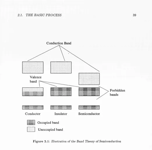
2.1 Illustration of the Band Theory of Semi conduction... 39
2.2 Thermodynamic arrangement of m icrocalorim eter... 41
2.3 Ideal output pulse from one X-ray e v e n t ... 45
2.4 A typical X-ray p u ls e ... 45
2.5 The amplification sy ste m ... 47
2.6 Electrical connections to an array of elements... 65
3.1 The Processed Simulated D a ta ... 87
3.2 Processing Flow C h a r t ... 93
4.1 FE1.19.11.DAT, no reje ctio n ...104
4.2 FE1.19.11.DAT, 90 rejection ... 104
4.3 FE1.19.11.DAT, no rejectio n ...106
4.4 FE1.19.11.DAT, 90 re je c tio n ...106
4.5 FE3.19.11.DAT, no reje ctio n ...108
4.6 FE3.19.11.DAT, 90 re je c tio n ...108
4.7 F E l.20.11.DAT, no reje ctio n ...110
4.8 FE1.20.11.DAT, 90 R e je c tio n ...110
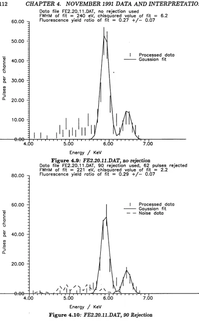
4.9 FE2.20.11.DAT, no rejectio n ...112
16 L IST OF FIGURES
4.10 FE2.20.11.DAT, 90 R e je c tio n ... 112
4.11 FE3.20.11.DAT, no rejectio n ... 114
4.12 FE3.20.11.DAT, 90 R e je c tio n ... 114
4.13 FE4.20.11.DAT, no rejectio n ... 116
4.14 FE4.20.11.DAT, 90 R e je c tio n ...116
4.15 FE5.20.11.DAT, no rejectio n ... 118
4.16 FE5.20.11.DAT, 90 R e je c tio n ...118
4.17 FE6.20.11.DAT, no rejectio n ... 120
4.18 FE6.20.11.DAT, 90 R e je c tio n ...120
4.19 FE7.20.11.DAT, no rejectio n ... 122
4.20 FE7.20.11.DAT, 90 R e je c tio n ...122
4.21 FE8.20.11.DAT, no rejectio n ... 124
4.22 FE8.20.11.DAT, 90 R e je c tio n ...124
4.23 FE10.20.11.DAT, no r e je c tio n ... 126
4.24 FE10.20.11.DAT, 90 R ejection...126
4.25 FE11.20.11.DAT, no r e je c tio n ...128
4.26 FE11.20.11.DAT, 90 R ejection...128
4.27 FE12.20.11.DAT, No re je c tio n ... 130
4.28 FE12.20.11.DAT, 90 R ejection...130
4.29 100 mK summed data, no r e je c tio n ... 132
4.30 100 mK summed data, 90 R e je c tio n ...132
4.31 200 mK summed data, no r e je c tio n ... 134
4.32 200 mK summed data, 90 R e je c tio n ... 134
4.33 FileN O ISE l.D A T ... 137
L IS T OF FIGURES 17
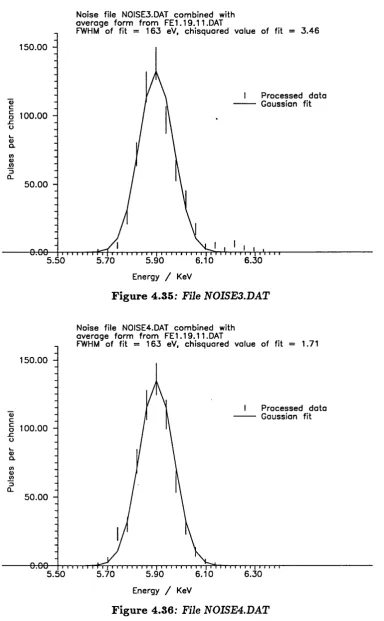
4.35 File N 0ISE3.D A T...138
4.36 File N 0ISE4.D A T...138
4.37 File N 0ISE5.D A T...139
4.38 File N 0ISE7.D A T...139
4.39 File N0ISE8.DAT . . . . * . ... 140
5.1 Standard Operation of an A D R ...160
5.2 Isothermal Operation of an A D R ...160
5.3 Cutaway schematic of Cochise A D R ...163
5.4 Thermal model of Cochise A D R ...167
7.1 Overview of Space-baaed A D R ... 198
7.2 Two stage ADR cycle... 201
7.3 Stage 1 of the Space A D R ... 202
7.4 The node structure of the System Thermal M o d e l... 206
7.5 Determination of absorbable energy density p s...213
7.6 Variation in Stage 2 hold time with pill m a s s ...217
7.7 Block D i a g r a m ... 221
L ist o f T ables
4.1 Source D a t a ... 99
4.2 Pulse rejection s t a t i s t i c s ... 142
4.3 FWHM R e s u lts ...143
4.4 Energy Histogram F i t t i n g ... 145
4.5 Fluorescence Yield R a t i o ... 146
4.6 Noise D a ta ... 147
5.1 Thermal model of Cochise A D R ... 168
7.1 GGG cooling e n e r g y ...212
7.2 Hold Time Available from Stage 2 ...218
7.3 ADR Control C y c le ... 224
Chapter 1
The History of X-Ray Calorimetry
1.1 Early History
W ithout doubt the very earliest calorimeters were the naturally occurring ones,
planets and satellites whose temperature rises by tens of kelvin due to internal
radioactivity. Interstellar particles of size 40 angstroms can rise in temperature
by as much as 200 K.
Calorimetry was first used in the early days of nuclear physics, for the measure
ment of the integrated energy of radioactivities, following Curie and Laborde’s
attem pts to verify that the heat produced from radioactive species resulted from
the absorption of emitted radiation. By the mid 1930s it was possible to op
erate small calorimeters at temperatures as low as 30 mK. The first composite
calorimeter was developed in the early 1970s at the Laboratoire de Physique Stel laire et Planétaire (LP5P), with a large surface area and a very small monolithic semiconductor.
In 1975, T.O. Niinikoski reported spurious heating, which he identified with the
passage of cosmic rays, but it was not until eight years later, in 1983, that work
began on single particle calorimetry. Several institutions including the Goddard
22 CHAPTER 1. THE H ISTO R Y OF X -R A Y C ALO R IM E TR Y
Space Flight Center ( GSFC) and the European Space Agency (ESA) started work around then, and by 1984, it was clear that thermal detectors cooled to very low
temperatures were going to be potential single event particle detectors of good
resolution.
1.2
Microcalorimetry In Context
Chapter 2 gives a detailed description of microcalorimetry in principle and prac
tice, however, it is worth, at this point, briefly surveying the range of currently
proven X-ray detectors, in order to show why X-ray microcalorimeters should be
developed, and to place them in their context.
1.2.1 Position Sensitive and Gas Scintillation Proportional Coun
ters
The earliest X-ray detectors are position sensitive and gas scintillation propor
tional detectors. The principle of operation of these devices is th at X-rays enter
a gas-filled cavity through a thin window, and may be incident on a gas molecule.
Usually this gas is xenon. Photoelectric absorption of the X-ray takes place which
excites the atom and releases a photo-electron. The atom de-excites by emitting
an X-ray or an Auger electron (see section 2.1.2), while the electron has sufficient
energy to ionise other gas molecules, and proceeds to do so until one electron-ion
pair is produced for each 30 eV of the original X-ray energy. In Position Sensitive
Proportional Counters (PSPCs) the electrons drift into a region of high elec
tric field where they are accelerated, and their increased energy liberates further
electron-ion pairs, usually increasing the number of free electrons by a factor of
over 10^. This process is referred to as an avalanche. Finally the electron cloud is
incident on the anode, and is registered by the amplification system. The energy
of the incident X-ray determines the size of the charge cloud produced, and hence
1.2. M IC RO C ALO RIM ETRY IN C O N TEXT 23
Unfortunately such a system is not particularly precise in its ability to determine
the energy of the incident X-ray, with 15 % being a typical energy resolution. This is so poor because of the statistical variance in the number of electrons liberated
by the incident X-ray, and also a similar variance in the number of electrons
generated in the avalanche stage. The quantum efficiency of such detectors,
however can be tailored to be near unity over a given an energy range. In the low
energy regime (1-2 KeV) the quantum efficiency is limited by X-ray absorption in
the window material, and in the high energy regime (10-20 KeV) the limitation
is posed by the increasing transparency of the gas. The window material can be
replaced by a plastic, which provides more transparency at low energy, making
detection at as low as 0.1 KeV possible, at the cost of a greater permeability for
the enclosed gas. At the high energy end it is possible to pressurise the gas to
a few atmospheres to decrease transparency, and hence enable operation up to
100 KeV. Position sensitivity in one axis can be developed by having multiple
anodes, and in the other axis by sensing how much charge “emerges” from each
end of the anode. Alternatively innovations such as the wedge and strip anode
allow spatial resolution as good as 150 /zm to be obtainable.
In the gaa scintillation proportional counter (GSFC) there is no high electric field
region to cause the charge avalanche. Instead electron clouds create light in a
region where the electric field is just sufficient to excite the gas. The scintillation
light generated is measured by an arrangement of photomultiplier tubes, which
determine X-ray energy by the total light intensity, and position by the relative
amount of light arriving at each tube. Because of the lack of the gas multiplication
avalanche stage, the energy resolution of GSPCs have a slightly improved energy
resolution of nearer to 9%, with measured values of 7% possible. The spatial
resolution of such a system is of the order of 900 ^m at 10 KeV, and is as low as
24 CHAPTER 1. THE H ISTO R Y OF X -R A Y C A LO R IM E TR Y
1.2.2 MicroChannel Plates
The microchannel plate (MCP) consists of a number of lead glass tubes bundled
together. The internal diameter of these tubes is usually around and
the center-to-center spacing 15/im. X-rays are incident perpendicular to the plate surface, and liberate photo-electrons. A high electric field is generated
between the opposite faces of the plate, and this causes the electrons to move
down the tubes, liberating further electrons en route. Usually two or more plates
are stacked up to create a cascade process where electron gains of 10^ are typical.
An electron cloud then emerges from the lower surface of the stack, and its
position is then located by an anode system, possibly of wedge and strip design
again.
The chief advantage of the microchannel plate system is that spatial resolution is
very high, and is limited only by the spacing and diameter of the tubes, hence a
value of 20 /im is typical. The quantum efficiency of such devices is high, however
the energy resolution is virtually non-existent.
1.2.3 Charge Coupled Devices
The charge coupled device (CCD) is an array of capacitors. Charge is deposited
on these capacitors by the incidence of X-rays, and is stored there until a ramped
electric field moves the rows of charge along to the edge of the array, where
they are read by an amplifier. The charge resultant from a single X-ray incident
on any of the pixels may be measured, and this is related to the energy of the
photon. Each of these metal-oxide-silicon capacitors is formed by the deposition
of electrodes on the surface of a silicon wafer, so the formed arrays are able to
resolve 30 fim spatially, and also possess an energy resolution of approximately 50 eV. The quantum efficiency of CCDs can be higher than that of a gas-filled
1.2. M IC RO C ALO RIM ETRY IN C O N TE XT 25
1.2.4 X-ray Micro calorimeters
The simplest X-ray microcalorimeter operates by the measurement of the rise
in tem perature of a semiconductor th at results from the incidence of an X-ray
photon. To avoid the complications that arise from X-ray thermalisation in a
semiconductor, a thermalising medium is often strongly bonded to the semicon
ductor, and used to convert the X-ray energy into thermal energy. The resistance
change of the semiconductor is measured by passing a small current through it,
and the change in this current yields the temperature change. When operated
at a tem perature as low as 100 mK, the theoretical limit for energy resolution is
estimated at 4eV, and FWHMs of 10 eV have already been observed. Position
resolution for these devices will depend on the development of arrays, however
an element width of less than 0.1 mm seems unlikely at this point. The quantum
efficiency of microcalorimeters is near-unity - for a given energy range of incident
X-rays it is possible to design the absorber in such a way as to absorb all incident
X-rays, with the only limitations being the small surface area, and the necessity
of keeping the heat capacity of the device, and hence the size of the absorber, as
small as possible.
1.2.5 Comparisons
Clearly the factor which is most in favour of X-ray microcalorimeters is the excel
lent energy resolution obtainable. However, despite the factor of 5 advantage of
the microcalorimeter over the CCD in terms of energy resolution, the spatial reso
lution of the CCD is approximately 5 times better than that of the microcalorime
ter, and hence is preferable in imaging applications, although for purely imaging
applications where no energy resolution is required, the microchannel plate would
appear to be the superior device. Compared to these three detector systems, the
proportional counters have been somewhat left behind by progress, with neither
the spatial resolution nor the energy resolution able to compete. The strongest
feature of each is only comparable with the weakest features of the microcalorime
26 CHAPTER 1. THE H ISTO RY OF X -R A Y C A LO R IM E TR Y
1.3 Review of Micro-calorimetry Work
1.3.1
GSFC
/
NASA Collaboration
In 1984[1] Moseley, Mather Sz McCammon suggested the use of a silicon arsenide wafer with a thermalising layer of aluminium as a spectrometer. The realisation
in work of the time th at at 300 mK such detectors are limited only by thermo
dynamic fluctuations in the system led to an increased urgency in such research,
and in their paper, the group proposed a suitable device. They estimated that
the theoretical limiting resolution for any such device is 1.1 eV FWHM.
In the same year [2], they demonstrated an antimony /boron-doped silicon detector
at 300 mK, with an ggFe source, and found a FWHM of 350 eV. This was reduced
to 270 eV by the elimination of multiple-pulse events. Theoretically, the group
estimated a resolution of 177 eV, and attributed the difference to amplifler noise
and the non-optimal flltering used.
The following year[3], the collaboration presented the results of experiments with
neutron transmutation doped germanium detectors at 300 mK, which yielded a
FWHM of 130-170 eV. Three different forms of support for the detector were used
in this run. In one case 0.3 mm brass wire was used, in another 1 mm quartz flbre
was used, and in the third a 1 mm bundle of superconductor-coated carbon flbre.
In the first and third cases the support was also used as the thermal/ electrical
link, whereas for the quartz support, 0.25 mm superconductor coated carbon fl
bre was used. The group also experimented with ion-implanted silicon, which has
the advantage of lower heat capacity, but experienced an unexpected broadening
of spectral lines, due to a varying amount of the photon energy being sensed in
events. The required solution was to detect all of the energy being deposited
by incident X-ray photons, and the need for a thermalising medium was recog
nised. Such a medium would consist of a material connected to the detector
semiconductor detector, acting to thermalise the incident X-ray.
Later in 1985[4] investigation moved towards the possibility of using X-ray mi
De-1.3. R E V IE W OF M ICRO-CALO RIM ETRY W O RK 27
magnetisation Refrigerator (ADR). The problem concerning the conversion of
X-ray energy to thermal energy in the detector was raised again, and the ma
terials gold and silver were considered for use as absorbers. However, the large
free-electron heat capacity of normal metals gave an unacceptably high level of
thermal noise, and a different material was considered. Bismuth was decided
upon, and a 2 ^m layer was evaporated onto the back of a silicon thermistor.
Tested with the ggFe source, this yielded a FWHM of 38 eV at a temperature of
98 mK.
In 1987[5], Mercury Cadmium Telluride (HgCdTe or MOT) was being used as the
thermalising element of a detector based on ion-implanted silicon. This detector
was connected to a 80 mK heat bath by 20 /zm aluminium wire, and demonstrated
a FWHM of 17.4 eV. This detector, used on the ggFe source, was able to demon
strate the separation of the g^Mn K a line into the K ai and K a2 elements. In this arrangement epoxy was used to connect the HgCdTe absorber to the silicon,
and made a large contribution to the heat capacity of the device. W ith this in
mind, consideration was given to the construction of a monolithic silicon detector.
A monolithic detector would be created by the implantation of phosphorus and
boron ions onto silicon wafer. Although this increases the specific heat capacity
of the material, it is possible to make it much smaller in size.
Further thought was given to the choice of absorber materials. HgCdTe is a
semiconductor, and had a 60meV bandgap in use, which seemed to give about
0.2 % broadening. Removing Cd from the compound would have eliminated this gap, but reduced the Debye temperature of the material to 140 K, thus making its
specific heat unacceptably high. Superconductors at less than one tenth of their
critical tem perature have negligably low electronic heat capacity, but deposited
energy tends to form long-lived quasi-particles.
In 1988[6] results showed a discrepancy between measured FWHM of pulses and
baseline noise of 11 eV in quadrature, and it was suggested that this was due
to charge-trapping in the HgCdTe being used as absorber. (Baseline noise is
the noise present in the detector which is present whether an X-ray is incident
28 CHAPTER 1. THE H ISTO R Y OF X -R A Y C A LO R IM E TR Y
of thermalisation.) Absorber material was addressed further, and an alternative
candidate suggested was the superconductor a-SnGe.
In 1992, the collaboration presented its results with Si detectors[7], where they
had achieved a FWHM of 10.3 eV with the jeFe source, applying some decon
volution processing. Some superconductors were suggested as suitable absorbing
media, and results with Tin were given.
The most recent publication from this collaboration[8] details efforts to devise a
1 element by 12 element array from a silicon wafer, and gives a newly obtained
deconvolved FWHM of 7.3 eV.
1.3.2
Lawrence Livermore National Laboratory (LLNL)
The work of this collaborative group developed from their involvement in infra-red
calorimetry.
In 1990[10], LLNL was working with neutron transmutation doped germanium (NTD Ge) as a resistive microcalorimeter, and was attempting to explain the
unexpected current-voltage behaviour of the material. In the same year a FWHM
of 19 eV was demonstrated by the group, which included 12 eV of electronic noise.
1.3.3
University o/London Collaboration
The earliest reference to the University of London collaboration on X-ray mi
cro calorimetry is in 1987. The collaboration originally grew from the interest of
(then) Queen Mary College in infra-red calorimetry, and the interest of Mullard Space Science Laboratory (a department of University College London ) in new X-ray detector technology. The University used a ^He cryostat to obtain tem
peratures in the region of 300 mK, and tested calorimeters optimised for use as
infra-red detectors with a g^Fe source. Initial results showed a FWHM of 357 eV,
with baseline noise of 330 eV.
From this point, the group developed an ADR with the assistance of Cochise
1.4. OTHER NEXT-G ENERATIO N X -R A Y D ETECTO RS 29
the same time as this was under development, E. Haller of LLNL supplied the collaboration with a sample of NTD Ge, which was used to build a 100 mK infra
red detector. Using this detector in a run in November 1991 showed that the
FWHM at 200 mK was 288 eV, with a baseline FWHM of 190 eV, and at 100 mK,
FWHM was 241 eV, with a baseline FWHM of 83 eV. Clearly the improvement
expected by a lower operating temperature had not been realised, and the reason
for this was suspected to be the presence of electron traps in the detector material.
To avoid these traps, it was proposed to deposit a layer of Tin onto the detector
surface, as a thermalising medium.
In 1992, Imperial College (IC) became involved in the collaboration as a result
of their involvement in dark m atter detectors. IC fabricate silicon detectors by
epitaxial chemical vapour deposition with Arsenic, which have an advantage over
germanium-based detectors in having a specific heat a factor of 100 lower.
1.4 Other Next-generation X-ray Detectors
1.4.1 Superconducting Tunnelling Junctions
Superconducting Tunnel Junctions (STJs) are similar in nature to microcalorime
ters in th at an X-ray imparts energy to a crystal, which then experiences a change
in its electrical properties. In the case of a superconductor below a its critical
tem perature the energy gaps between bands axe as small as, for example 3 meV
in niobium, as compared to about 1 eV for semiconductors, and so a vast number
of free electrons axe created by the impact and thermalisation of an X-ray. The
limitation of statistical variation in the number of charge-carriers produced, there
fore is somewhat reduced. The initial photo-absorption causes the creation of a
number of quasi-particle chaxge-caxriers, each of an energy greater than 100 meV,
which then emit phonons as a mechanism of losing energy. Since the Debye en
ergy is much greater than the superconductor energy gap, the phonons produced
in the X-ray interactions with chaxge-caxriers can themselves produce chaxge-
30 CHAPTER 1. THE H ISTO R Y OF X -R A Y C ALO R IM E TR Y
loss.
The result of this is that the resolution possibility of such a device is statistically
set by the number of charge-carriers created, as detailed in Section 2.4.7, and in
the case of STJs could therefore be as low as a resolution of 4eV.
In practice, the method used for determining* the number of free charge carriers
available in the material is to use a quantum mechanical approach. Two over
lapping layers of the superconductor are separated by a thin insulating layer. A
bias voltage is applied across the outer layers, and tunnelling allows a current
to pass between them. The level of this current is determined by the density of
charge carriers present. Charge carrier density is affected by the deposition of
energy associated with an X-ray impact for a few microseconds, and hence the
bias current through the junction can be monitored.
Finkbeiner et al[12] worked with aluminium STJs, and in 1991 claimed resolutions
of 3.3 % with the ggFe source, which correlates to about 200 eV, at 276 mK. Hûbner
et al[ll] used a niobium device, and achieved a resolution of 100 eV in 1993.
1.4.2 Dielectric Microcalorimeters
The development of dielectric microcalorimeters [13] arose chiefly out of the desire
to have the high resolution of resistive microcalorimeters, but without the atten
dant Johnson noise. Dielectric detectors consist of a material with temperature-
dependent dielectric properties. The X-ray thermalisation energy is imparted to a
dielectric material, which forms the dielectric layer in a capacitor. The measure
ment of the induced change in capacitance yields the temperature change after
calibration has been established, and one can proceed to analyse the temperature
curve as with a resistive microcalorimeter.
A paper produced by the Centre in 1988[9] addressed the idea of applying then
current calorimetry techniques to the X-ray field. This paper acknowledges the
failings of thermistor-type calorimeters in use as X-ray microcalorimeters, and
1.4. OTHER N EXT-G ENERATIO N X -R A Y D ETECTO RS 31
this application, citing some predicted detector performances which showed that
a dielectric solution would have at least a factor of two improvement in FWHM.
The highest resolution the paper conceived for a dielectric was 3eV, and more
interestingly, predicted that a FWHM of 17 eV should be obtainable at 300 mK,
which would obviate the problems addressed later in this thesis of cooling in a
space environment - only a pumped ^He dewax would be required.
The eaxly calculations of the LLNL group suggested th at a dielectric device operated at 300 mK would offer a similar resolution to a resistive device op
erated at 100 mK. The initial tests made on the ferroelectric material KTN
(KTai_a.NbxO3,x =0.1 2) were with infra-red LED pulses and 6 MeV alpha par
ticles, and so little can be inferred from these results for the future implications
of this device in X-ray detection, however it was clear th at a non-thermal mech
anism was responsible for the detection of alpha particles, and this phenomenon
would have to be further explored before the device could become viable.
1.4.3 Kinetic Inductance Microcalorimeters
Kinetic inductance thermometers are another development from the LLNL which exploits the temperature dependence of Kinetic Inductance (KI). KI arises from
the inertial mass of Cooper pairs in a superconductor, and the quantity of pairs
present in a superconductor is dependent on the ambient temperature, hence
kinetic inductance is a good measure of temperature. The device constructed by
the LLNL consists of an iridium groundplane at 104 mK, on a diamond substrate. The dielectric over the groundplate was silicon monoxide, and the top layer was
a niobium stripline. To absorb X-rays a slab of niobium was attached to the
underside of the diamond substrate. The exact construction of the device and the
choice of operating temperature is dependent on the heat capacity of the device,
the maximum energy X-ray to be studied, and the required energy resolution.
Whilst signal from the detector is maximized by operating at a temperature as
close to the critical temperature as possible, it is essential th at the energy of any
32 CHAPTER 1. THE H ISTO R Y OF X -R A Y C A LO RIM ETRY
critical temperature, which in the case of this detector is 110 mK.
Various amplification systems are considered for this device, including a DC bias
supported by a Superconducting Quantum Interference Device (SQUID), which
requires reducing the efficiency of the thermal link between the absorber and the
detector proper, to reduce the data rate from the detector to the electronics. An
other amplification system operates on AC, and is essentially a potential divider,
with the detector and a bias resistor in series, and a FET amplifier buffering the
output impedance. In a third configuration, the inductance of the detector is
used as part of a tuned circuit, and altering the inductance alters the resonance
frequency, which is determined by a phase-locked loop. This is the system which
B ib lio g ra p h y
[1] Thermal Detectors as X-ray Spectrometers - S.H. Moseley, J.C. Mather, D. McCammon, J. Appl. Phys., Vol.56 No.5 pp. 1257-1262, September 1984.
[2] Experimental Tests of a singlephoton calorimeter fo r Xray Spectroscopy
-D. McCammon, S.H. Moseley, J.C. Mather, R.F. Mushotzky, J. Appl. Phys.,
Vol.56
[3] Thermal Detectors as Single Photon X-ray Spectrometers - S. Harvey Mose ley, R.L. Kelley, J.C. Mather, R.F. Mushotzky, A.E. Szymkowiak, D. Mc
Cammon, IEEE Transactions on Nuclear Science, Vol. NS-32 No.l pp. 134-
138, February 1985.
[4] The GSFC/Wisconsin X-ray Spectroscopy Investigation fo r A X A F - S.S. Holt, R.L. Kelley, S.H. Moseley, R.F. Mushotzky, A.E. Szymkowiak, D. Mc
Cammon, M. Juda, J. Zhang, in Second International Symposium on Optical and Electro-Optical Science and Engineering pub. December 1985.
[5] Thermal Detectors fo r High Resolution Spectroscopy - D. McCammon, M. Juda, J. Zhang, S.S. Holt, R.L. Kelley, S.H. Moseley, A.E. Szymkowiak,
Japanese Journal of Applied Physics, Vol.26, Supplement 26-3, 1987.
[6] Advances towards High Spectral Resolution Quantum X-ray Calorimetry - S.H.Moseley, R.L. Kelley, R.L. Schoelkopf, A.E. Szymkowiak, D. McCam
mon, J. Zhang, IEEE Transactions on Nuclear Science, Vol.35 No.l pp.59-64,
February 1988.
34 B IBLIO G R AP H Y
[7] X-ray microcalorimeters - principles and performance - S.H. Moseley, M. Juda, R.L. Kelley, D. McCammon, O.K. Stable, A.E. SzymkowiaJc, J. Zhang,
Proceedings of an ESA Symposium on Photon Detectors for Space Instru
mentation, at Noordwijk 10-12 November 1992, ESA SP-356, pp.13-19
[8] Thermal Calorimeters fo r high resolution X-ray spectroscopy - D. McCam mon, W. Cui, M. Juda, J. Morgenthaler, J. Zhang, R.L. Kelley, S.S. Holt,
G.M. Madejski, S.H. Moseley, A.E. Szymkowiak, Nucl. Inst. Meth. A326
(1993) pp.157-165
[9] A New Microcalorimeter Concept for Photon Counting X-ray Spectroscopy - Eric H. Silver, Simon E. Labov, F. Goulding, N. Madden, D. Landis, J. Beeman, Nuclear Instruments and Methods in Physics Research, Vol. A277
pp.657-663, 1989.
[10] Electrical and Thermal properties of neutron-transmutation-doped Ge at 20 m K - Ning Wang, F.C. Wellstood, B. Sadoulet, E.E. Haller, J. Beeman, Physical Review B, Vbl.41, No.6, pp.3761, 15 February 1990-11
[11] Superconducting Tunnel Junctions as Photon Counting Detectors - P. Hiibner, N. Rando, A. Peacock, P. Videler, A. van Dordrecht, J. Lumley,
EUV, X-Ray and Gamma-Ray Instrumentation for Astronomy IV (Proceed
ings from SPIE’s Annual Meeting in San Diego, 1993)
[12] Superconducting aluminium tunnel junctions with indium absorbers fo r low-energy X-ray spectroscopy - F. Finkbeiner, A. Hahn, W. Heeringa, P. Jany, H.O. Klages and T. Strobelt, Nuclear Instruments and Methods in Physics
Research A306, pp.215-219, 1991
[13] Test results of a prototype dielectric microcalorimeter - T.E. Pfafman, E. Silver, S. Labov, J.Beeman, F. Goulding, W. Hansen, D. Landis, N. Madden,
SPIE Vol. 1344 pp.302, EUV, X-Ray, and Gamma-Ray Instrumentation for
B IB LIO G R A P H Y 35
[14] Position Sensitive Detectors in X-ray Astronomy - J.L. Culhane, Nuclear Instruments and Methods in Physics Research A310 (1991) 1-13, pp.l
[15] Development o f X-ray Calorimetric Detectors and Data Processing Tech niques at London University - I.D. Hepburn, P.A.R. Ade, M.J. Griffin, W.S. Holland at Queen Mary College, and J.L. Culhane, R. Kessel, D.M. Walton
at Mullard Space Science Laboratory, University College London, in the book
Low Temperature Detectors for Neutrinos and Dark M atter-II published by
Frontières^ 1988. Edited by L. Gonzalez-Mestres and D. Perret-Gallix.
[16] Thermal Detectors fo r X-ray Astronomy - Stephen S. Holt, Pub. Laboratory for High Energy Astrophysics, NASA/GSFC, Greenbelt, MD, USA, 1989(7).
[17] Superconducting Tunnelling Junction Detectors - A. Zehnder, C.W. Hagen, W. Rothmund, SPIE Vol.1344 pp.286, EUV, X-Ray, and Gamma-Ray In
strumentation for Astronomy 1990
[18] Application of kinetic inductance thermometers to x-ray caloHmetry - Yolanda C. Wai, Simon E. Labov, Eric H. Silver, SPIE Vol. 1344 pp.314,
EUV, X-Ray, and Gamma-Ray Instrumentation for Astronomy 1990
[19] D. Twerenbold, 1986, Europhys. Letts 1. (1986), 209-214
[20] H. Kraus, C. Jochum, B. Kemmather, M. Gutsche, F. v.Feilitzsch, R.L.
Chapter 2
Principles of X-ray Microcalorimetry
2.1 The Basic Process
2.1.1
Semiconductivity, The Band Theory of Solids
The band theory of solids is a means of understanding the transport of electrons.
When atoms are clustered closely together, the energy level diagrams for each
atom become distorted, such that they axe perturbed away from the normal levels.
Hence in the system, an energy level in a group of atoms spreads to become an
energy band. Higher energy valence levels become the widest bands, whereas
lower levels, closer physically to the atoms they pertain to, axe less affected by
the electric fields of other atoms, and axe spread less. The situation in conductors
is th at there is a partially filled band such that electrons can pass from one atom
to another with only the slight amount of energy supplied by an electric field. In
insulators and semiconductors a band, called the valence band, is completely full.
This means that electrons cannot move about, since movement to a neighbouring
atom would mean moving to an already occupied state, which is not allowed. The
difference between semiconductors and insulators is that, in semiconductors, the
next level up, the conduction level, is very close to the valence level, a gap of 1 eV
38 CHAPTER 2. PRINCIPLES OF X -R A Y M ICRO CALO RIM ETRY
or less. At finite temperatures the thermal energy imparted to electrons allows
them to jump into the conduction band. These three conditions are illustrated
in Figure 2.1.
In the cases of silicon and germanium, the atoms are arranged into tetrahedral
structures, and covalent bonds are formed between neighbouring atoms. A small
amount of energy (1.1 eV for Si, 0.7 eV for Ge) is required to break one of these
bonds and free an electron. This is the energy gap between the valence and
conduction bands. At room temperature, therefore, a large number of electrons
axe freed, and this number increases rapidly with temperature. The hole left by a
vacated electron will be filled by a neighbouring electron, and the hole left there
will also be filled, so th at the hole also travels. The hole serves as a positive
charge carrier. In pure semiconductors there are as many holes as electrons, and
this is referred to as intrinsic conductivity.
Extrinsic conductivity occurs when an impurity is introduced, for example if
some arsenic (group V) is added to some molten germanium. As has five valence
electrons, and hence the loose one in a Ge structure has a bonding energy of only
0.01 eV. This electron easily escapes and becomes free charge. There is no hole,
however, so only the electron is the charge carrier. At normal temperatures very
few Ge atom electrons can escape and conduct, so even a 1 in 10^° concentration
of As makes the As electrons the majority carrier, and the material is called an
n-type semiconductor.
On the other hand, if gallium, a group III element with three valence electrons
is used, then the atom steals an electron from neighbouring atoms, and forms a
hole, which is mobile. This type of semiconductor is then called p-type, since the
positively charged holes are the majority carriers.
At very low temperatures, for example below 300 mK, conduction in semicon
ductors occurs by a slightly different means. At this temperature charge carriers
are frozen out, or trapped on dopant sites. If the impurity concentration is care
fully chosen, then the energy gap between sites is only just too great for charge
2.1. THE BASIC PROCESS 39
Conduction Band
Valence band
Forbidden bands
Conductor Insulator
Occupied band
Unoccupied band
Semiconductor
Figure 2.1: Illustration o f the Band Theory o f Sem iconduction
hopping”, which occurs when a high energy phonon imparts energy to the charge
carrier. This means that conduction in the material is a strong function of the
number density and average energy of phonons present, and hence of tempera
ture. The resistance of a doped material in this regime depends very strongly on
the dopant concentration.
It can be seen from this that semiconductors make exceptionally good thermome
ters, and they have been in use for many years as detectors of infra-red radiation.
In these detectors, a wafer of semiconductor is connected to a heat sink at a low
40 CHAPTER 2, PRINCIPLES OF X -R A Y M ICRO CALO RIM ETRY
heats the wafer. By passing a bias current through it, it is possible to deter
mine the resistance of the wafer, and with suitable calibration the amount of
energy incident on the wafer is determinable. From this and filters to determine
the frequency of photons permitted to reach the detector, the tem perature of
astronomical sources may be measured.
In X-ray microcalorimetry, a similar setup is used, but the received energy is from
individual X-ray photons, rather than a continuous flux of infra-red radiation.
2.1.2 The Thermalisation of X-rays
When an X-ray is incident on an atom of, for example germanium, it causes the
release of a photo-electron, or an Auger electron.
(Auger electrons are the result of energy being imparted to a K-shell electron.
The K-shell electron is emitted, and an L-shell electron takes its place. The
photon emitted by the transition is absorbed by an electron in the same atom,
probably in the L-shell, ejecting it. In this way no radiation escapes from the
atom, just two electrons, hence this is called a radiationless transition.)
These high energy electrons (or electron in the case of photo-electron emission)
then lose their energy to phonons and electrons by repeated interactions with
the lattice. The phonons then relax to an equilibrium distribution, which is
observed as a rise in temperature. Since the wafer is connected to a heat sink,
the temperature of the wafer then drops as the heat leaks to the sink.
In practice the arrangement shown in Figure 2.2 is also used. The X-ray is
incident on an absorbing medium, which has a good thermal link to a piece of
semiconductor, and quickly reaches thermal equilibrium with it. If the combined
heat capacity of the medium and the semiconductor is represented by C, and the
2.1. THE BASIC PROCESS 41
Incident x-ray energy A E
Good thermal link Heat capacity C
-■S^îcoridüctôr Crystal
Thermal Link Conductance G
Heat Sink
Figure 2.2: Therm odynam ic arrangement o f m icrocalorim eter
The raised temperature of the medium-semiconductor combination causes heat
to flow to the heat sink along the thermal link with conductance G. In practice this thermal link is often the sense wires used to paas a hiaa current through the
semiconductor, and hence determine its resistance.
By considering the rate of energy flow from the detector to the sink, it can be
shown that the time taken for the detector to return to the heatsink temperature
42 CHAPTER 2. PRINCIPLES OF X -R A Y M IC RO C ALO RIM ETRY
approximately by the equation
r/„" - g
A proof of this follows.
A conductive link exists between the detector and the bath such that energy
passes from the detector to the sink as defined by this equation.
dQ = - A T G d t
where
• Q is the amount of energy present in the material responsible for the temper
ature excess over the bath. Initially this will be AE^ the energy deposited by the X-ray incidence. dQ is the change in this energy due to the thermal conduction between the detector and the bath in time dt.
• A T is the temperature difference between the detector and the bath A T =
Td—Th where Td is the detector temperature, and Ti is the bath temperature.
• G is the thermal conductance between the detector and the bath.
Above it has been shown that A T = where A E is the energy of the incident X-ray. In the same manner, the difference in temperature between the detec
tor and the bath is dependent on the amount of energy Q remaining from this incidence, ie. A T = Hence substituting this into the above.
dQ — ——Gdt
Hence
2.1. THE B A SIC PROCESS 43
And
Q
ln(Q) = ——t + constant
C/
We are free to define this constant as In(üf), hence
(-§■)
In order to determine the constant K , use the boundary condition th at at time t = 0, Q = A E — C A T . Hence
Q = A E. exp
Since A T =
or
A T — To exp
We can define Tfaii = § , and obtain
44 CHAPTER 2. PRINCIPLES OF X -R A Y MICRO C ALO RIM ETRY
Hence in time r/azz, the pulse height will have fallen to 37% of its initial height.
This fall time is the major restriction on the event rate the detector can register,
and is in the region of 1 ms, hence yielding an upper limit for event rate of about
1000 counts/second, and a more realistic limit of 100 counts/ second in order to
reduce the probability of more than one X-ray event co-inciding.
In fact, because the connections between the detector and the amplifier have
a finite capacitance between them, of the order of 4pF , and the amplifier has
an input capacitance of 3pF, the pulse shape output from the amplifier has a
risetime Triac which is dependent on this total capacitance and the resistance of the detector. The pulse which is observed is then of the form
where
• jR is the resistance of the detector.
• C is the total capacitance between the signal transmission lines.
• Triae IS the rise time constant, the product of R and C.
W ith a typical detector resistance of 30 MH and a total input capacitance of
7pF, the rise-time constant is of the order of 0.2 ms, compared to a fall time
of approximately 0.5 ms, and such a pulse is shown in Figure 2.4. The effect
of this rise-time is to reduce the peak height of the pulse, and this hence limits
resolution.
It can be shown by differentiation that the time at which the pulse reaches its
peak is given by
tp —
---'^riae "^fall
In this case the combination of capacitance and resistance causes the peak height
of the pulse to be only 31.3% of that which would be the case if either the
2.1. THE B ASIC PROCESS 45
A
température of detector
AT
time
Figure 2.3: Ideal output pulse from one X-ray event
1000.00
A Typical p u lse from 0 lOOmK d e te c to r
800.00
.? 600.00 0) .c
0) jn 3
Q.
400.00
200.00
0.00
200 400 600 800 1000 1200
-200
Time a fter th erm alisation (m ic r o s e c o n d s )
46 CHAPTER 2. PRINCIPLES OF X -R A Y M ICRO CALO RIM ETRY
2.1.3 The Hot Electron Effect
The theory of electron-phonon decoupling, or the hot electron effect was first pro
posed by Wang et al[l] to explain the non-linearity in current-potential difference
characteristic of semiconductors at low temperatures. Previous work had been
done by other authors describing this effect as it applied to metals.
Thermal equilibrium between the electrons and phonons in a material depends on
the continuous exchange of phonons between electrons, and this is only possible
if there are a number of final states available for electrons to descend into when
emitting a phonon, or to rise into upon absorption.
The incidence of an X-ray upon the semiconductor, or the thermal conduction of
heat from an absorber to the semiconductor affects the electrons in the material
initially, and if the phonons are unable to reach thermal equilibrium with the
electrons then the process of phonon-assisted hopping, the principal means of
electrical conduction at this temperature will be retarded, and the dependence of
resistance on temperature will be less strong. In the case of an X-ray incidence
the large amount of energy deposited in the small area affected means that a
large number of phonons are created initially, and this problem is less acute.
The hot electron effect is temperature dependent, and seems not to occur at
temperatures as high aa 100 mK.
2.1.4 Observation
In order to observe the effect of the X-ray on the detector, it is necessary to pass
a small bias current through the semiconductor wafer, typically of the order of
1 nA. The electrical potential drop across the detector will be dependent on the
resistance of the semiconductor, and this is put through a series of amplifiers, so
that it can be digitised and recorded.
Figure 2.5 shows the system of amplification used by the University of London
collaboration. The bias resistor and the bolometer are both in the 100 mK en
2.1. THE B ASIC PROCESS 47
COLD MODULE—
o BIAS
TEST INPUT
■O +9V lOOK lOOK
OUTPUT BIASRESISTC
FET
12K BOLOMETER
INSIDE ADR
Figure 2.5: The ampllhcation system
potential divider the two form down. The output of the FET is then put through
a capacitor to remove the DC bias, and then through a pair of non-inverting
amplifiers with a cascade gain switchable between 200 and 1000.
The digitisation stage can be performed by a digital storage oscilloscope, giving
its output through an IEEE port, or by a simpler analogue to digital converter
48 CHAPTER 2. PRINCIPLES OF X -R A Y M IC RO C ALO RIM ETRY
2.2 Example System
2.2.1 Description
In the case of the X-ray microcalorimetry program developed by the University of London collaboration, the original material used was Neutron Transmutation Doped germanium (NTD Ge) supplied by E. Haller from the Lawrence Livermore Laboratory. The original sample[8] had dimensions of 0.12 mm X 0.10 mm X
0.30 mm, and an associated heat capacity calculated at 349 mK of 6.8pJ.K “ ^.
Hence the incidence of a 6 KeV photon on the sample would cause a temperature
increase of 0.00014 K or 0.14 mK.
2.2.2 Bolometer Characteristics
The ideal resistance for the bolometer is between 30 MÎÎ and 40 Mf2. The bias re
sistor is typically 120 Mil or 240 Mfi, and a current of ideally 1 nA passes through
the potential divider arrangement. If a detector has too great a resistance, then
it has a high level of Johnson noise. Whilst increasing the current through the
detector raises the temperature, and reduces the resistance to a more acceptable
level, the temperature increase will cancel the advantage gained.
Additionally, a high resistance causes an increase in the pulse rise-time, as illus
trated in Section 2.1.2, and reduces the peak height of the observed pulse.
Operating at a lower resistance, however, means that the resistance change with
temperature will be less. The resultant change in potential difference across the
detector will consequently be smaller, and the device resolution is diminished.
The bolometer resistance is therefore one of the most critical parameters of the
device - too low a resistance and the resistance change with temperature drops,
too high and the Johnson noise of the detector becomes more significant, and the
rise time of the pulse is lengthened, making the pulse height lower.
The sample was indium-soldered to two 15//m diameter brass wires of 1.50 mm
2.2. EXAM PLE SYST E M 49
circuits, and also provide the thermal contact with the heat sink. In the early
experiments a ^He dewax was pumped on to obtain a heat bath of 300 mK, while
in later years an Adiabatic Demagnetisation Refrigerator was supplied by Cochise Inc., which enabled bath temperatures of 100 mK to be achieved. This is further discussed in Chapter 5.
2.2.3 Amplification Electronics
In this system, the ADR and the amplification electronics were enclosed in a large
faraday cage, with a substantial earth, to eliminate the electrical interference from
the substantial amount of electronic equipment present in the laboratory.
Electrical connections inside the ADR were made by high purity copper wire,
lacquered to the cold surface by Ge varnish, but are now free-floating to avoid
capacitance, a limitation to resolving power as described in Section 2.1.2.
2.2.4 Computer Simulation
As an diagnostic tool it was decided to develop a computer program to simulate
the operation of a resistive X-ray microcalorimeter, based on the University of London device. The main features of this model included
• A simulation of the effect of varying tem perature and current on the re
sistance of the germanium detector. This was achieved by recording the
current-volt age curve of a sample at various temperatures, and using an
extrapolation to calculate intermediate values.
• A calculation of the effect of bias current on the base tem perature of oper
ation of the detector. This was achieved by calculating the heating effect
based on the power product VI.
• The rise in temperature of the detector due to the incidence of an X-ray
50 CHAPTER 2. PRINCIPLES OF X -R A Y M ICRO CALO RIM ETRY
sample at the base temperature, and assuming th at the X-ray energy is
imparted instantaneously to the detector.
• The thermal connection between the detector sample and the heat bath was
calculated from real data. By measuring the time constant of a real X-ray
pulse as shown in Figure 2.3, it is possible to determine the conductance of
the thermal link.
2.3 The Effects of Different Materials
Two materials have shown their respective merits in use as thermometers in
X-ray microcalorimetry. Below I discuss the materials, methods used for their
preparation, and the pros and cons of each of them.
2.3.1 Germanium
The University of London collaboration to date has used this material in the fabrication of its X-ray and infra-red microcalorimeters. The standard procedure
for the doping of germanium with impurities is to bombard the material with a
stream of thermal neutrons. Germanium has a number of stable isotopes present
in its natural form, and these decay into dopant impurities after absorbing thermal
neutrons. The dopant concentration is determined by the neutron flux, and to
remove the damage caused by fast neutrons, thermal annealing is used. This
means of preparation has been shown to yield a highly uniform concentration
rivalled only by ion implantation.
In order to use the detector it is necessary to make an electrical contact to it,
and this has to date been done by indium dots and gold wire, with a small speck
of arsenic between the germanium and indium. A problem with this is that the
change in contact area with repeated soldering leads to varying R-T curves, and
the need to recalibrate. Future contacts will be ion-implanted, with mettalisation