
ISSN (e): 2250-3021, ISSN (p): 2278-8719
Vol. 04, Issue 02 (February. 2014), ||V5|| PP 34-43
An Overview of Reconfigurable Hardware for Efficient Implementation of
DSP Algorithms
Mahesh Kadam
1, Kishor Sawarkar
21(M.E Student, Department of Electronics & Telecommunication, Rajiv Gandhi Institute of Tech.,
Mumbai University, India) ([email protected])
2
(Asst.Professor, Department of Electronics & Telecommunication, Rajiv Gandhi Institute of Tech., Mumbai University, India) ([email protected])
Abstract: - Reconfigurable hardware is emerging as the best option for the efficient implementation of complex and computationally expensive signal processing algorithms. Reconfigurable hardware exploits the benefit of high of computational efficiency of hardware as well as flexibility of software implementation. Field Programmable Gate Array (FPGA) which finds wide range of applications in the field of signal processing, wireless communication, image and video processing has gained popularity as a reconfigurable logic over past decade. In this paper, various hardware aspects of reconfigurable such as architectures and models including external coupling and run-time reconfigurable systems have been studied. Moreover, a case study of most widely used commercial FPGA technologies from Xilinx and upcoming three dimensional 3D- FPGA architecture is presented. It is revealed that the reconfigurable hardware can be used in a variety of DSP applications. FPGA implementation of digital signal processing applications show enhanced outcome in terms of speed as compared to software implementation and previously reported architecture.
Keywords: - Field Programmable Gate Array (FPGA), Reconfigurable Hardware, Signal Processing.
I.
INTRODUCTION
There are two methods for the implementing digital signal processing applications. The first method is hardware technology like Application Specific Integrated Circuit (ASIC) which offer higher performance, since they are designed for specific computation. Hardware adapts to the application, but cannot re-adapt to a new application. However, redesign and re-fabrication is required if any modification in the circuit. The second approach is software programmed processors which provides flexible solution using software development tools. Designer customizes application depending on available resources. However, limitation is that the performance is affected due to high execution overhead.
Reconfigurable Computing offers advantages of both hardware technology and software programmed processor i.e. compromise between performance and flexibility as shown in Fig. 1. Field Programmable Gate Array (FPGA) due to its internal architecture offers best option for reconfigurable computing. FPGAs consist of an array of logic blocks, I/O pads and routing channels to implement complex digital computations. These resources are useful for achieving parallelism, specialization and flexibility of many DSP applications.
figure 1. DSP implementation spectrum [1]
of DSP applications discussed DSP applications on FPGA with improved performance as compared to their software implementation is discussed.
II.
COMPUTING USING RECONFIGURABLE HARDWARE
Reconfigurable computing system consists of processor and reconfigurable unit for efficiently implementing systems with high degree of parallelism. For reconfigurable system development interconnection should be very efficient and development of design and compilation tools for mapping on reconfigurable hardware. In section we discussed about reconfigurable hardware architecture, coupling methods and FPGA technology.
2.1
RECONFIGURABLE HARDWARE2.1.1
ARCHITECTURESReconfigurable systems are often classified according to the coupling techniques between the reconfigurable unit and the processor. Compton and Hauck [2] present the classifications shown in Fig. 2. First architecture, the reconfigurable unit is in the form of one or more standalone devices. To communicate with the reconfigurable unit same I/O mechanisms of the processor are used. In this configuration, the data transfer is relatively slow. Next configuration in Fig. 2, show attached processing unit and Coprocessor with cheaper communication cost than that of the architecture with standalone unit. Work without intervention of host processor, reconfigurable unit and host processor works simultaneously. There is delay in communication between host processor and attached processor but gives independence computation. Fourth configuration shows an architecture in which the reconfigurable unit is part of the processor itself. They are very tightly coupled which adds instruction for programming. Fig. 3 shows the processor is embedded in the programmable unit. The processor can either be a „hard‟ core or can be a „soft‟ core which is implemented using the resources of the programmable fabric itself.
figure 2 Different architecture of reconfigurable system. Reconfigurable logic is shaded [2].
figure 3 Processor embedded in a reconfigurable fabric [2].
2.1.2
RECONFIGURABLE FUNCTIONAL UNITSReconfigurable functional unit structures can be classified as either fine grained or coarse grained. Fine grained structure means functions defined using single or number of bits, such as look up table for implementing logic. Fig.4a [3] shows implementing of three inputs single function, cluster of LUT is shown in Fig.4b [3]. Fig.5 shows logic block architecture of virtex5 which has six inputs LUT [4]. Coarse grained structure which may consist of arithmetic and logical unit with memory element for implementing logic, primarily planned for word width data path optimization. An example of coarse grained architecture ADRES shown in figure 6 [5], which contains 32 bit ALU less flexible but very efficient. Fine grained structure has more area, delay and power overhead has compared to coarse grained structure. Another structure, Heterogeneous arrays where property of logic is not same throughout the system which provide flexibility and greater performance. Heterogeneity is provided by embedding multiplier block within reconfigurable hardware [6, 7, 8]. Heterogeneous structure example with embedded memory blocks within reconfigurable unit, look up table
Programmable unit
RAM structure, dedicated memory block. Modern FPGA almost all architecture contains embedded storage unit [8].
figure 4 Fine-grained reconfigurable functional units [3] a Three-input lookup table
b Cluster of lookup tables
figure 5 Logic block architecture [4] Virtex-5 6-input LUT architecture
figure 6 ADRES reconfigurable functional unit [5]
2.2
FPGATECHNOLOGYA field-programmable gate array (FPGA) is an integrated circuit designed to be configured by a designer after manufacturing hence "field-programmable" [9]. FPGA offers various features such as floor planning enables resources allocation within FPGA to meet these time constraints. The ability to update the functionality after shipping, partial re-configuration of a portion of the design and the low non-recurring engineering costs relative to an ASIC design.
programmable routing is also configured to make the necessary connections between logic blocks and from logic blocks to I/O blocks. The processing power of an FPGA is depends on the processing capabilities of its logic blocks and the total number of logic blocks available in the array. Fig. 7 (b) [10] shows the architecture of a simple logic block containing one four input LUT and one flip-flop for storage. Logic blocks are sometimes designed to allow them to be efficiently used as local memory and shift registers, and they generally contain dedicated carry circuitry in order to simplify implementation of adders and multipliers.
figure 7 [10] (a) Architecture of a generic FPGA. All FPGAs include the basic elements shown here. Newer FPGAs may also include embedded memory blocks, dedicated multiplier blocks, and even processor cores. (b) Simplified architecture of a logic block showing one, four-input lookup table (LUT). Each LUT can synthesize any four-input logic function, and may also be specialized for implementation of memory and shift registers. Newer FPGAs may contain as eight or more LUTs in single logic block.
Benefits of FPGA technology [11]
Performance: Taking advantage of hardware parallelism, FPGAs exceed the computing power of digital signal processors (DSPs) by breaking the paradigm of sequential execution and accomplishing more per clock cycle. Controlling inputs and outputs (I/O) at the hardware level provides faster response times and specialized functionality to closely match application requirements.
Time to market: FPGA technology offers flexibility and rapid prototyping capabilities in the face of increased time-to-market concerns. You can test an idea or concept and verify it in hardware without going through the long fabrication process of custom ASIC design. Reconfiguration is possible on an FPGA design within hours instead of weeks. The growing availability of high-level software tools decreases the learning curve with layers of abstraction and often offers valuable IP cores (prebuilt functions) for advanced control and signal processing.
Cost: The nonrecurring engineering (NRE) expense of custom ASIC design far exceeds that of FPGA-based hardware solutions. The large initial investment in ASICs is easy to justify for OEMs shipping thousands of chips per year, but many end users need custom hardware functionality for the tens to hundreds of systems in development. The very nature of programmable silicon means you have no fabrication costs or long lead times for assembly. Because system requirements often change over time, the cost of making incremental changes to FPGA designs is negligible when compared to the large expense of re-spinning an ASIC.
Long-term maintenance: As mentioned earlier, FPGA chips are field-upgradable and do not require the time and expense involved with ASIC redesign. Digital communication protocols, for example, have specifications that can change over time, and ASIC-based interfaces may cause maintenance and forward-compatibility challenges. Being reconfigurable, FPGA chips can keep up with future modifications that might be necessary. As a product or system matures, you can make functional enhancements without spending time redesigning hardware or modifying the board layout.
III.
RECONFIGURABLE HARDWARE FOR DSP
3.1 DSPSYSTEM IMPLEMENTATION
Reconfigurable computing platforms for DSP offer an intermediate solution to ASICs, PDSPs, and general and domain-specific processors by allowing reconfigurable and specialized performance on a per application basis. Reconfigurable hardware offers tradeoff between performance, cost, power, flexibility and design effort (NRE). Table 1 [1] shows different DSP implementation.
Table 1. DSP implementation comparison. [1]
Performance Cost Power Flexibility Design
effort(NRE)
ASIC High High Low Low High
Programmable DSP Medium Medium Medium Medium Medium
General Purpose
Processor Low Low Medium High Low
Reconfigurable
Hardware Medium Medium High High Medium
Reconfigurable hardware for DSP, the benefits which can be used to fulfill the goals of DSP applications can be reviewed as follows:
Specialization: Programmable digital signal processor works sequentially, now most of DSP processor contains parallel VLIW and multi-function unit for implementation algorithm to achieve better performance [12]. Reconfigurable devices contain memory (LUT‟s) and interconnect switch, application programs in the form of bit streams can be downloaded on fabric that is to say any modification re-implemented without expensive NRE cost with improved performance.
Reconfigurability: Configuration after post fabrication on run time is beneficial for DSP application implementation. DSP system needs configurability under different constraints, means for direct benefit using hardware platform are field customization, slow adaptation and fast adaptation.
Parallelism: Reconfigurable device FPGA with fine-grained parallelism which offers distributed computation for high sample rates, beneficial for variety of signal processing applications such as image and speech processing. FPGA enables pipelined implementations using internal flip-flops for high system clock rates. Using FPGA, resource utilization and speed of adaptation for power reduction in signal processing applications is possible. Most of modern commercial FPGA‟s includes embedded unit, memory for parallel access to data for distributed computation [13, 14]. A case study of modern FPGA‟s discussed in next section.
3.2 DSP SYSTEM USING FPGA
Various DSP applications have been mapped to reconfigurable device with the benefits discussed in previous sections and recent research focused on dynamic reconfiguration and dedicated architecture, most work on use of application parallelization and specialization. In this section some of the DSP applications that have been mapped to FPGA device are described.
Reconfigurable FIR Filter Architecture: Wireless communication systems require the reconfigurable fir filter architecture. In this proposed architecture complexity degraded by the coefficient multipliers. In [15], using proposed coefficient representation method, hardware requirements for multiplexer are reduced. Two reconfigurable FIR filters based on 4-bit partitioning were designed and synthesized using ALTERA QUARTUS II, synthesis result show 39% area reduction in resource usage and 15% power reduction over previously reported architecture.
computes each tap in one clock cycle and hardware implementation, N taps computed in parallel in one clock cycle.
Embedded Systems & Image Processing: In [17] presents advantages and limitation of FPGA technology, its suitability for image processing and computation. The advantages are reconfigurability, the ability to exploit parallelism. The limitations are conversion of algorithms to fixed point representation. Author discussed research direction towards FPGA technology.
Video & Audio processing: video processing requires large bandwidth and processing capability to handle data from analog video equipments. The Programmable Active Memories PAM system [18] first platform for video applications. Audio processing requires less bandwidth than video processing, audio application can benefit from specialization, a sound synthesizer implemented using PAM system [18] producing real time audio of 256 different voices at up to 44.1 kHz. In [19] three different architectures for implementing a least mean square (LMS) adaptive filtering algorithm, using a 16 bit fixed-point arithmetic representation is shown. These architectures are implemented using the Xilinx multimedia board as an audio processing system. A comparison between the three architectures shows that a total speedup of 3.8 times. This improvement comes at a cost of extra area and lower level of flexibility. Using a pure HW architecture results in a speedup of 82.6 times with a moderated area, and lower flexibility.
IV.
CASE STUDY OF XILINX FPGA ARCHITECTURES
Due to the parallel nature, high frequency, and high density of modern FPGAs they make an ultimate platform for the implementation of computationally intensive and massively parallel architecture. This section presents a case study of FPGAs from Xilinx. These include Spartan-6, Virtex-7, Virtex ultra scale and Kintex ultra scale FPGAs.
Spartan-6 FPGAs
Spartan-6 FPGA delivers an optimal balance of low risk, low cost, and low power for cost-sensitive applications, now with 42% less power consumption and 12% increased performance over previous generation devices [14]. Spartan-6 FPGAs the thirteen-member family with half the power consumption of previous Spartan families, and faster, more comprehensive connectivity. Built on a 45 nm low-power copper process technology that delivers the optimal balance of cost, power, and performance, Increased Memory Block Capacity to 4.8Mbits, Integrated Memory Controllers, up to 180 Efficient DSP48A1 Slices, GTP Transceivers in Spartan-6 LXT: 100Mbps to 3.2Gbps, Optimized Power Saving Modes, Embedded Processing. Spartan-6 FPGA Family comprises of two domain-optimized sub-families as follows:
Spartan-6 LX FPGAs are optimized for applications that require the absolute lowest cost. They support up to 147K logic cell density, 4.8Mb memory, integrated memory controllers, DSP slices, ease-of-use, and high-performance Hard IP with an innovative open standards-based configuration.
Spartan-6 LXT FPGAs extend the LX family to deliver up to eight 3.2Gbps GTP transceivers and an integrated PCI Express Block, both derived from proven Virtex FPGA family technology, to provide the industry‟s lowest-risk and lowest-cost solution for serial connectivity.
Xilinx 7 series FPGAs
Xilinx 7 series FPGAs comprise three new FPGA families that address the complete range of system requirements, ranging from low cost, small form factor, cost-sensitive, high volume applications to ultra-end connectivity bandwidth, logic capacity, and signal processing capability for the most demanding high-performance applications.
The 7 series FPGAs include:
Artix-7 Family: Optimized for lowest cost and power with small form-factor packaging for the highest volume applications.
Kintex-7 Family: Optimized for best price-performance with a 2X improvement compared to previous generation, enabling a new class of FPGAs.
Virtex-7 Family: Optimized for highest system performance and capacity with a 2X improvement in system performance. Highest capability devices enabled by stacked silicon interconnect (SSI) technology.
Table 2: 7 Series Families Comparison [14]
Maximum Capability Artix-7 Family Kintex-7 Family Virtex-7 Family
Logic Cells 215K 478K 1,955K
Block RAM 13Mb 34Mb 68Mb
DSP Slices 740 1,920 3,600
Peak DSP Performance 929 GMAC/s 2,845 GMAC/s 5,335 GMAC/s
Peak Transceiver Speed 6.6 Gb/s 12.5 Gb/s 28.05 Gb/s Peak Serial Bandwidth
(Full Duplex) 211 Gb/s 800 Gb/s 2,784 Gb/s
PCIe Interface X4 Gen2 X8 Gen2 X8 Gen3
Memory Interface 1,066 Mb/s 1,866 Mb/s 1,866 Mb/s
I/O Pins 500 500 1,200
I/O Voltage 1.2V, 1.35V, 1.5V,
1.8V, 2.5V, 3.3V
1.2V, 1.35V, 1.5V, 1.8V, 2.5V, 3.3V
1.2V, 1.35V, 1.5V, 1.8V, 2.5V, 3.3V
Xilinx Ultra Scale series FPGAs
Xilinx Ultra Scale architecture comprises two high-performance FPGA families that address a vast spectrum of system requirements with a focus on lowering total power consumption through numerous innovative technological advancements.
The family includes:
ASIC-like clocking for scalability, performance and lower dynamic power Next generation routing for rapid timing closure & industry leading performance Enhanced logic infrastructure for maximum performance and device utilization
Ultra Scale architecture-based FPGAs are arranged in a column-and-grid layout. Columns of resources are combined in different ratios to provide the optimum capability for the device density, target market or application, and device cost. Figure 8 shows a device-level view with resources grouped together. For simplicity, certain resources such as integrated blocks for PCI Express, Configuration logic, and System Monitor are not shown. The Ultra Scale architecture-based FPGAs have one or two columns of transceivers.
figure 8 figure 9 figure 8: FPGA with Columnar Resources [14]
figure 9: Column-Based FPGA Divided into Clock Regions [14]. For graphical representation only, does not represent a real device
Resources within the device are divided into segmented clock regions. The height of a clock region is 60 CLBs. A bank of 52 I/Os, 24 DSP slices, 12 blocks RAMs, or 4 transceiver channels also matches the height of a clock region. The width of a clock region is essentially the same in all cases, regardless of device size or the mix of resources in the region, enabling repeatable timing results. Each segmented clock region contains vertical and horizontal clock routing that span its full height and width. These horizontal and vertical clock routes can be segmented at the clock region boundary to provide a flexible, high-performance, low-power clock distribution architecture. Figure 9 is a representation of an FPGA divided into regions.
Virtex Ultra Scale FPGAs: The industry's most capable high-performance FPGAs enabled using both monolithic and next generation SSI technology to achieve the highest system capacity, bandwidth, and performance. Variants of the Virtex Ultra Scale family are optimized to address key market and application requirements through integration of various system-level functions, delivering unprecedented embedded memory and serial connectivity capabilities. Virtex Ultra Scale devices provide unprecedented levels of performance, system integration and bandwidth and are ideal for a wide range of applications such as 400+ Gb/s systems, large-scale emulation and high performance computing. These devices deliver a step-function in increased bandwidth and reduced latency for systems demanding massive data flow and packet processing.
Table 3: Ultra Scale Series Families Comparison[14]
Range Kintex Ultra Scale Virtex Ultra Scale
Logic Cells (K) 355–1,160 627–4,407
Block Memory (Mb) 19.0-75.9 44.3-115.2
DSP (Slices) 1,700–5,520 600–2,880
DSP Performance (GMAC/s) 8,180 4,268
Transceivers 16–64 36–104
Peak Transceiver Speed (Gb/s) 16 33
Peak Serial Bandwidth (full duplex) (Gb/s) 2,086 5,101
PCIe Interface 2–4 2–6
Memory Interface Performance (Mb/s) 2,400 2,400
I/O Pins 312–832 364–1,456
I/O Voltage 1.0–3.3V 1.0–3.3V
Virtex Ultra Scale 16nm FinFET
In addition to Kintex and Virtex Ultra Scale devices built on TSMC‟s 20nm SoC process technology, Xilinx will also be offering Virtex Ultra Scale All Programmable devices built on TSMC‟s 16nm FinFET process technology to deliver aggressive power savings and performance improvements.
figure10: Xilinx Multi-Node Product Portfolio Offering [14]
V.
3D-FPGA ARCHITECTURE
figure11 Abstract view of the 3-D FPGA architecture [22]
Stacked silicon interconnect (SSI) technology
SSI technology solves the challenges that had previously obstructed attempts to combine the interconnect logic of two or more FPGAs to create a larger, “virtual FPGA” for implementing a complex design. These challenges include: Limited Connectivity, Excessive Latency, Power Penalty, and Signal Integrity for High-Speed Serial Connectivity.
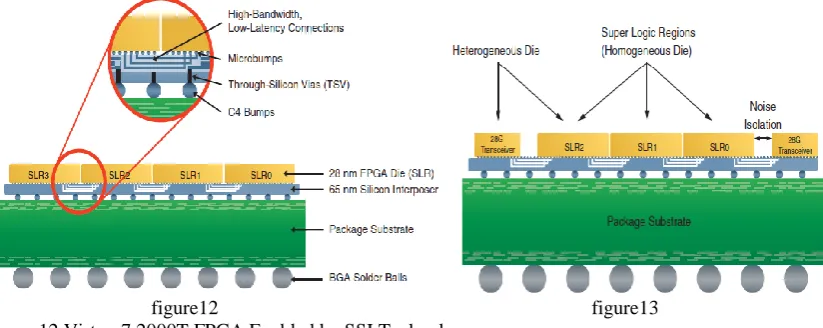
To address these challenges of interconnecting multiple FPGAs, 3D IC devices utilize Stacked Silicon Interconnect technology, enabling high-bandwidth connectivity between multiple die and providing a 100x improvement in inter-die bandwidth per watt compared to multi-chip approaches. It also imposes much lower latency and consumes dramatically lower power than either the multi-FPGA or multi-chip module approach, while enabling the integration of transceivers and on-chip resources within a single package. SSI technology leverages proven micro bump technology combined with coarse pitch through-silicon vias (TSVs) on a passive (no transistors) 65nm silicon interposer to deliver high reliability interconnect without performance degradation on one FPGA device. This breakthrough technology provides the next level of advanced system integration for applications that require high logic density and tremendous computational performance. Figure 12 shows the side view of the die stack-up with four FPGA SLRs, silicon interposer, and package substrate. In Figure 13, the Virtex-7 H870T FPGA ties together three SLRs as well as separate 28G capable transceiver circuits via the silicon interposer.
figure12 figure13 figure 12 Virtex-7 2000T FPGA Enabled by SSI Technology
figure 13 Heterogeneous 3D FPGA with Integrated 28G Transceivers
Xilinx All Programmable 3D ICs utilize stacked silicon interconnect (SSI) technology to break through the limitations of Moore‟s law and deliver the capabilities to satisfy the most demanding design requirements. Xilinx homogeneous and heterogeneous 3D ICs deliver the highest logic density, bandwidth, and on-chip resources in the industry, breaking new ground in system-level integration.
Xilinx 3D IC Devices Utilizing Stacked Silicon Interconnect Technology
Table 4: Xilinx 3D IC Devices Utilizing SSI Technology [14]
Kintex Ultra Scale XCKU100* XCKU115*
Virtex Ultra Scale XCVU125* XCVU145* XCVU160* XCVU440*
Virtex-7 T 7V2000T*
Virtex-7 XT 7VX1140T*
Virtex-7 HT 7VH580T** 7VH870T**
*Homogeneous **Heterogeneous
VI.
CONCLUSION
Reconfiguration hardware provides a viable option for DSP system designers and DSP algorithm developers for the efficient implementation of DSP algorithms. This work presents extensive review of highly developed FPGA architectures and technologies which can be utilized to achieve high performance and efficient FPGA-based circuits and systems. Adaptive Noise Canceller (ANC) and its implementation is reviewed thoroughly for the experimental validation. The experimental results ensure the high-speed FPGA architecture. Reconfigurable FIR filter architecture has been also presented using proposed coefficient representation. The synthesis results of the designed architecture shows area and power optimization. FPGA implementation will be more flexible and effective for digital signal processing systems.
VII.
ACKNOWLEDGEMENT
The author would like to thank the following for valuable discussions related to this work: Dr.S.S.Mande, S.D.Patil and M.K.Ahirrao.
REFERENCES
[1] R.Tessier ,W.Burleson, Reconfigurable Computing for Digital Signal Processing : A Survey , Journal of VLSI Signal Processing 28, 2001, 7–27.
[2] K.Compton, S.Hauck, Reconfigurable computing: a survey of systems and software, ACM Comput. Surv., 34, (2), 2002, pp. 171–210.
[3] T.J. Todman, G.A. Constantinides, S.J.E. Wilton, O. Mencer, W. Luk and P.Y.K. Cheung, Reconfigurable computing: architectures and design methods, IEE Proc.-Comput. Digit. Tech., Vol. 152, No. 2, March 2005. [4] Xilinx, Virtex-5 FPGA family overview, DS100 (v5.0) February 6, 2009.
[5] Mei, B., Vernalde, S., Verkest, D., De Man, H., and Lauwereins, R. ADRES: An architecture with tightly coupled VLIW processor and coarse-grained reconfigurable matrix, Lect. Notes Comput. Sci., 2778, 2003.
[6] Haynes, S. D. And Cheung, P. Y. K. A reconfigurable multiplier array for video image processing tasks, suitable for embedding in an FPGA structure. IEEE Symposium on Field Programmable Custom Computing Machines, 1998, 226–234.
[7] Chameleon Systems, Inc. 2000. CS2000 Advance Product Specification. Chameleon Systems, Inc., San Jose, CA. [8] Syed Qasim, Shuja Abbasi, Advanced FPGA Architectures for efficient implementation of computation intensive
algorithms: A State-of-Art Review, MASAUM Journal of Computing, September 2009. [9] http://en.wikipedia.org/wiki/Field-programmable_gate_array
[10] W. James MacLean, An Evaluation of the Suitability of FPGAs for Embedded Vision Systems. Computer Vision and Pattern Recognition - Workshops, 2005. CVPR Workshops. IEEE Computer Society Conference on 25 June 2005. [11] National Instruments white paper, Introduction to FPGA Technology: Top 5 Benefits, Apr 16, 2012. www.ni.com
[12] Texas Instruments Corporation, http://www.ti.com/lsds/ti/dsp/overview.page
[13] Altera Corporation, www.altera.com
[14] Xilinx Corporation, www.xilinx.com
[15] Mahesh Ketha, CH. Venkateswarlu, Design & FPGA Implementation Of Reconfigurable FIR Filter Architecture For DSP Application, International Journal of Engineering Research & Technology (IJERT), Volume 1 Issue 7, Sep. 2012.
[16] Tian Lan, Jinlin Zhang, FPGA Implementation of an Adaptive Noise Canceller, International Symposiums on Information Processing (ISIP), 2008.
[17] W. James MacLean, An Evaluation of the Suitability of FPGAs for Embedded Vision Systems. Computer Vision and Pattern Recognition - Workshops, 2005. IEEE Computer Society Conference on 25 June 2005.
[18] J. Vuillemin, P. Bertin, D. Roncin, M. Shand, H. Touati, and P. Boucard, Programmable Active Memories: Reconfigurable Systems Come of Age, IEEE Transactions on VLSI Systems, vol. 4, no. 1, pp. 56–69, March 1996. [19] A. Elhossini, S. Areibi and R. Dony, An FPGA Implementation of the LMS Adaptive Filter for Audio Processing, in
Proc. IEEE International Conference on Reconfigurable Computing and FPGAs, pp.1-8, Sept. 2006. [20] 3-D FPGA from tezzaron. <http://www.tezzaron.com/about/PhotoAlbum/ Products/3DFPGA.html>
[21] “Xilinx stacked silicon interconnect technology delivers breakthrough FPGA capacity, bandwidth, and power efficiency”, by Kirk Saban White Paper: Virtex-7 FPGAs WP380 (v1.2) December 11, 2012.
![figure 1. DSP implementation spectrum [1]](https://thumb-us.123doks.com/thumbv2/123dok_us/8354809.1668377/1.595.122.366.552.686/figure-dsp-implementation-spectrum.webp)
![figure 3 Processor embedded in a reconfigurable fabric [2].](https://thumb-us.123doks.com/thumbv2/123dok_us/8354809.1668377/2.595.226.335.493.592/figure-processor-embedded-in-a-reconfigurable-fabric.webp)
![figure 5 Logic block architecture [4] Virtex-5 6-input LUT architecture](https://thumb-us.123doks.com/thumbv2/123dok_us/8354809.1668377/3.595.132.447.100.640/figure-logic-block-architecture-virtex-input-lut-architecture.webp)
![figure 7 [10] (a) Architecture of a generic FPGA. All FPGAs include the basic elements shown here](https://thumb-us.123doks.com/thumbv2/123dok_us/8354809.1668377/4.595.188.403.157.387/figure-architecture-generic-fpga-fpgas-include-basic-elements.webp)
![Table 2: 7 Series Families Comparison [14] Artix-7 Family Kintex-7 Family](https://thumb-us.123doks.com/thumbv2/123dok_us/8354809.1668377/6.595.71.525.686.774/table-series-families-comparison-artix-family-kintex-family.webp)
![figure 8: FPGA with Columnar Resources [14] figure 9: Column-Based FPGA Divided into Clock Regions [14]](https://thumb-us.123doks.com/thumbv2/123dok_us/8354809.1668377/7.595.77.516.379.535/figure-columnar-resources-figure-column-based-divided-regions.webp)
![Table 3: Ultra Scale Series Families Comparison[14] Range Kintex Ultra Scale](https://thumb-us.123doks.com/thumbv2/123dok_us/8354809.1668377/8.595.88.507.404.589/table-ultra-scale-series-families-comparison-range-kintex.webp)
![Table 4: Xilinx 3D IC Devices Utilizing SSI Technology [14] XCKU100* XCKU115*](https://thumb-us.123doks.com/thumbv2/123dok_us/8354809.1668377/10.595.75.519.82.177/table-xilinx-devices-utilizing-ssi-technology-xcku-xcku.webp)
