Dynamic Power Reduction Using Clock Gating: A Review
1
Himanshu Chaudhary,
2Nitish Goyal,
3Nagendra Sah
1,2,3PEC University of Technology, Chandigarh, UT, India
Abstract
The clock pulses are responsible for up to 70 % of dynamic power dissipation in a synchronous circuit. The synchronous design operates at high frequency that drive a large load because it has to reach many sequential elements throughout the chip. Thus clock has been a great source of power dissipation because of high frequency and load. Clock signal do not perform any computation and mainly used for synchronization. Hence these signals are not carrying any information. So by using clock gating one can save power by reducing unnecessary clock activities inside the gated module. In this paper we go through various clock gating schemes.
Keywords
Low Power, Clock Gating, Dynamic Power Reduction
I. Introduction
There are three performance parameters on which a VLSI designer have to optimize the design i.e. Area, Speed and Power. Today’s consumer demands more functionality, small size, high speed and optimized power devices.
Dynamic power dissipation is the main source of power dissipation in CMOS circuits.
P = αfCV2
Where α is switching activity at the nodes
Consumer demands a smaller size battery with longer life. To do so power have to be minimized at each levels . To optimize power the simplest technique is to shut down the clock supply for those blocks of the sequential circuit which remains idle or not used for long period. Up to 70% or even more of the dynamic power can be spent in the clock buffers. This result makes intuitive sense since these buffers have the highest toggle rate in the system. In addition, the registers receiving the clock dissipate some dynamic power even if there is absolutely no change in input and output. Clock Gating: Clock gating is one of the well known and effective power optimization technique in VLSI circuits. Its aim is to suppress the propagation of transitions within the circuit under
some conditions satisfied by clock gating circuitry. The main source
of power dissipation in circuits are due to charging and discharging of the capacitors. So if the transitions, switching activities at the nodes decreases and the power dissipation reduces. This switching activities are reduced by gating those blocks which are idle at that time and hence avoiding unnecessary wastage of power in the
form of charging and discharging of node capacitances.
Clock gating is particularly useful for registers that need to maintain the same logic values over many clock cycles. The main
challenges of clock gating are finding the best places to use it and
creating the logic to shut off and turn on the clock at the proper times. Register-Transfer Level (RTL) becomes the most proper
stage where power optimization has significant impact and power
estimation is accurate [1, 5].
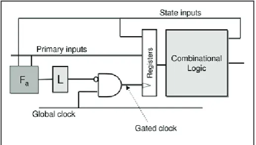
Fig. 1: Basic Clock Gating Cell
II. Various Clock Gating Schemes Available
A. AND Gate Based
Fig. 2: AND Based Clock Gating
In simple AND gate based scheme[2] the enable signal explicitly control the clock input to the logic block. Here if enable signal goes inactive between the clock pulse, clock output prematurely terminates(hazard problem). Or if En goes multiple times on and off between clock pulses then it generates multiple clock pulses. This restriction makes this circuit inappropriate.
Fig. 4: Correct Output When Counter is Positive Edge Triggered.
Fig. 5: Hazard Problem When AND Based Clock Gating is Used
B. Latch Based Technique
The latch based clock gating style adds a level-sensitive latch to the design to hold the enable signal from the active edge of the clock until the inactive edge of the clock. The anomaly occurs when enable signal changes during the sleep period leading to an incorrect design. Here hazard problem that exits in AND gate design is removed but glitch problems is still there.
Fig. 6: Latch Based Clock Gating
C. Flip-Flop Based Clock Gating
This technique is similar to latch based design with one difference
that instead of latch, D flip flop is used here. The same anomaly
which existed in latch based design exists here too with longer sleep period. So the probability of missing the change on the enable pin is high. Therefore this technique is not used much. Also area overhead increases much in comparison to latch based technique.
Fig. 7: DFF Based Clock Gating
D. Mux Based Clock Gating
In this technique the feedback path is controlled by the mux. Mux is controlled by mux select line when it is required to close or open the feedback path. This circuit is simple robust and often a reasonable choice. But this circuit uses one fairly expensive mux per bit and consume more power.
Fig. 8: MUX Based Clock Gating
Some advanced clock gating schemes [4]:
1. Clock Gating Without Enable Signal (Data Driven) These techniques reduces the power consumption by taking into account the switching activity of the circuit.
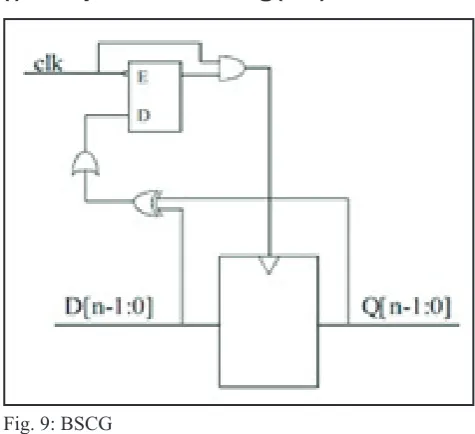
Bus Specific Clock Gating (BSC). •
Threshold based clock gating (TCG).
•
Optimized bus specific clock gating (OBSC). •
(i). Bus Specific Clock Gating (BSC)
This techniques is used here for n bit data [6]. If input and output of n bit register is same than output of xor gate is 0 otherwise 1. Similarly for OR gate if any input bit is 1 than output is 1. Here OR gate is used to determine if any bit change takes place. So in this way the register is safely gated by latch and AND gate without allowing any glitch to reach the register clock. However power consumption will be high if output toggle rate increases which indicates high switching activity[3] of the signal.
(ii). Threshold Based Clock Gating (TCG)
This is a data driven clock gating technique in which a threshold is considered which is 5%(example) of the switching activity. So the FF having toggle rate less than 5% needs to be clustered using one clock gating cell. The toggle rates of FFs of non-clock
gating circuit need to be tested at first time, and then according
to the list of toggle rate, those FFs are divided into two parts. In this way disadvantages of BSC technique is removed.
(iii). Optimized Bus- Specific Clock Gating (OBSC)
This is a fine grained activity-driven CG methodology which is
used to improve BSC as well. This technique uses the relationship
between the flip flop for clustering them unlike TCG. The problem
of gated FF selection is reduced from exponential complexity into linear. It works by comparing the inputs and outputs and gates the clock when they are equal.
Fig. 10: OBSC
Considering N FFs in the non-CG circuit, each FF can be chosen as gated or non gated. Hence, 2N CG solutions are possible and the exponential complexity problem is reduced into linear. Assume that all the FFs are chosen to be gated initially, then the problem is in determining which FFs should be excluded from gating. Heuristically, the FF with the maximum output data
toggle rate should be excluded from gating first. This is because
that maximum output data toggle rate indicates that minimum clock toggles will be gated, thus power will reduce least or even increase if the FF is gated. More formally, the FF with the
maximum output toggle rate is excluded from gating first, then
the FF with the second largest output toggle rate is excluded and so on until all the FFs are excluded (i.e., the original non CG circuit). Apparently, during the process of exclusion, there will be N+1 possible CG solutions which is linear complexity.
2. Clock Gating With Enable Signal Local explicit clock gating (LECG).
•
Enhanced clock gating (ECG).
•
Single comparator based clock gating (SCCG).
•
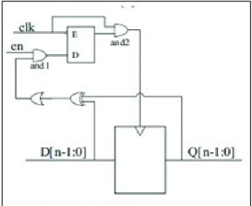
(i). Local Explicit Clock Gating (LECG)
Fig. 11: LECG
Here clock of Flip flop is gated explicitly by using enable signal.
This enable signal increase the control of the circuit explicitly.
Here as long as en=0 no clock is passed of flipflop and hence
no power consumption, but power consumption starts when en
is high i.e 1. If en=1 period is significantly high than over all
power consumption increase due to additional circuitry which overweighs the savings.
(ii). Enhanced Clock Gating (ECG)
This method combines both BSCG and LECG and make use of the advantages of both methods like in BSCG switching activity increase the power dissipation which is eliminated by using en signal which gated the circuit for that much period of time. But if aforementioned situation is not emerged then this method consume more power because of complex circuit than previous to methods.
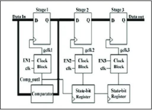
(iii). Single Comparator-Based Clock Gating (SCCG) This is an example of 3-stage pipeline in SCCG technique [7] structure. It consists of 3 parts:
Fig. 13: SCCG
Data Path: For each stage in the data path, there is a regular register triggered by gated clock signal gclk. All the data-path registers are connected successively forming the basic pipeline structure.
Clock Blocks: At each stage, there is a clock block generating gated clock signal gclk for data-path register. The input of the clock block are global clock signal clk, stage enable signal EN, and the comparison result Comp_outcoming from either comparator or state-bit register.
Comparator & State-bit Registers: This part is the most important and novel part of the new proposed technique. At the 1st stage, the comparator is inserted, which has 3 duties:
Evaluate the consistency between the input data and output 1.
data at the 1st stage. If there is no change occurred, its output signal Comp_outis reset to logic “0”; otherwise, it is set to logic “1”.
Send the Comp_outsignal to the current stage’s clock block 2.
in order to generate local clock signal. Pass the Comp_outsignal to the next stage. 3.
III. Limitations of Clock Gating
The main problem is the timing of the clock signal and the 1.
ability to group latches with identical gating conditions.
Sometimes it is difficult to reach the timing closure if the
2.
clock gating signal have larger fan out and it is driving many clocks if the latch group is very large.
It also does not consider the possibility of one part of the 3.
functional unit is in use while the other is not in use. In traditional clock gating , it does not take into account the 4.
switching activities of the registers it involves.
Clock gating reduces test-coverage of the circuit because 5.
clock gated registers are not clocked until the enable signal is high.
IV. Conclusion
In this paper various basic as well as advanced clock gating techniques are discussed. We discuss four basic techniques
using AND gate, Latch, flipflop and mux and their advantages
and disadvantages.
Also 6 types of advanced gating schemes are discussed which are
classified on basis of enable signal in two groups. These techniques
are used when we consider n number of registers. In advanced techniques various ways of grouping the registers to whom same clock is supplied are discussed.
References
[1] Smitha Sundaresan, Frederic Rivoallon,“Analysis of Power Savings from Intelligent Clock Gating”, XAPP790 (v1.0) Xilinx August 13, 2012.
[2] Jagrit Kathuria, M. Ayoubkhan, Aarti Noor,“A review of clock gating techniques” MIT International Journal of Electronics and Communication Engineering, Vol. 1 2 Aug 2011, pp.106-114.
[3] Frederic Rivoallon,“Reducing Switching Power with Intelligent Clock Gating’’, WP370, Xilinx, August 29, 2013.
[4] Yunlong Zhang, Qiang Tong, Li Li, Wei Wang, Ken Choi, JongEun Jang, Hyobin Jung, Si-Young Ahn,“Automatic Register Transfer Level CAD Tool Design for Advanced Clock Gating and Low Power Schemes”, ISOCC 2012, pp. 21-24.
[5] L. Li, K. Choi,"Activity-driven optimized
bus-specific-clock-gating for ultra-low-power smart space applications", IET Commun., 2011, Vol. 5, Issue 17, pp. 2501–2508.
[6] T. Lang, E. Musoll, J. Cortadella,"Individual flip-flops with
gated clocks for low power datapaths", IEEE TCAS-II: Analog and DigitalSignal Processing, 44(6), 1997.
[7] W. Wang, Y. C. Tsao, K. Choi, S. Park, M. K. Chung, "Pipeline power reduction through single comparator-based clock gating", SoC Design Conference (ISOCC), 2009 International, pp. 480-483.
Prof. Nagendra Sah was born in Jaynagar, India, on 05-01-1960. He is Assistant Professor in PEC University of Technolgy ( Formerly PEC-Deemed University), Chandigarh, India. He has done his B.Tech degree in Electronics and Communication Engg. from National Institute of Technolgoy, Warangal, Andhra Pradesh, India in 1986 and Master of Engg. Degree in Electronics Engg. From Panjab University, Chandigarh, India in 2005. He has teaching experience of about 18 years. Presntly, he is working as Assistant Professor. He has published about 40 papers in national and international conferences and in international journals. His research is focused on the radio-system design, wireless communication and networking and modeling of mobile radio propagation and the development of simulation methods for a mobile radio channels.