Implementation of a FFT using High Speed and
Power Efficient Multiplier
1
Padala.Abhishek.T.S,
2Dr. Shaik.Mastan Vali
1,2Dept. of ECE, MVGR College of Engineering, Vizianagaram, Andhra Pradesh, India
Abstract
Fast Fourier Transform (FFT) is used to convert a signal from Time domain to frequency domain and this is needed so that you can view the frequency components present in the signals. A Fourier Transform converts a wave in the time domain to the frequency domain. An FFT is an algorithm that speeds up the calculation of a DFT. In essence, an FFT is a DFT for speed. The entire purpose of an FFT is to speed up the calculations.
The Decimation- In-Time radix-2 FFT using butterflies has designed. The butterfly operation is faster. The outputs of the
shorter transforms are reused to compute many outputs, thus the
total computational cost becomes less. An FFT is a very efficient
DFT calculating algorithm. For the design of FFT the some of the different modules are used mostly Adders and Multipliers plays an important role in the design of FFT. The overall performance of the FFT is based on the throughput of the Multiplier. Here the multiplier with AHT is used to reduce the power consumption and to increase the speed of the FFT.
Keywords
Fast Fourier Transform (FFT), Discrete Fourier Transform (DFT), Decimation in Time (DIT), Adaptive Hold Technique (AHT)
I. Introduction
The Fast Fourier Transform (FFT) is a discrete Fourier transform algorithm which reduces the number of computations needed for N points from 2N6 to 2N log N, where log is the base-2 logarithm. FFTs were first discussed by Cooley and Tukey (1965), although
Gauss had actually described the critical factorization step
as early as 1805 (Bergland 1969, Strang 1993). A discrete
Fourier transform can be computed using an FFT by means of the Danielson-Lanczos lemma if the number of points N is a power of two. If the number of points N is not a power of two, a transform can be performed on sets of points corresponding to the prime factors of N which is slightly degraded in speed.
An efficient real Fourier transform algorithm or a fast Hartley transform (Bracewell 1999) gives a further increase in speed by approximately a factor of two. Base-4 and base-8 fast Fourier transforms use optimized code, and can be 20-30% faster than base-2 fast Fourier transforms. Which means a 1024 sample FFT is 102.4 times faster than the “straight” DFT. For larger numbers
of samples the speed advantage improves. Prime factorization is slow when the factors are large, but discrete Fourier transforms
can be made fast for N=2, 3, 4, 5, 7, 8, 11, 13, and 16 using
the Winograd transform algorithm.
Fast Fourier transform algorithms generally fall into two classes:
decimation in time, and decimation in frequency. The Cooley-Tukey FFT [2] algorithm first rearranges the input elements in
bit-reversed order, and then builds the output transform (decimation
in time). The Sande-Tukey algorithm (Stoer & Bulirsch 1980) first transforms, then rearranges the output values (decimation in
frequency). This paper is based implemented in the Decimation
in Time class. Before going in detail with DIT FFT here are the
basic terms to understand the FFT Implementation i.e. Danielson-Lanczos Lemma (D-L Lemma) is required for long equation
writing, but it’s a vital component of the FFT, Twiddle factor wNn , Butterfly Algorithm where the Butterfly diagram is a diagrammatic
representation of an FFT algorithm and Reverse bit pattern for data input.
A. Danielson-Lanczos Lemma (D-L Lemma)
The Danielson-Lanczos Lemma (D-L Lemma) equation for FFT is given as
Here the DFT is broken up into two summations of half the size of the original. The first summation is the “even terms”
i.e. & the second is the
“oddterms”i.e. .
W is the “twiddle factor”.
B. Twiddle factor (W)
Twiddle factor is given by .
C. Reverse Bit Format
A bit-reversal permutation is a permutation of a sequence of n
items, where n = 2k is a power of two. It is defined by indexing the elements of the sequence by the numbers from 0 to n-1 and
then reversing the binary representations of each of these numbers. Each item is then mapped to the new position given by this reversed value. The bit reversal permutation is an involution, so repeating the same permutation twice returns to the original ordering on the items.
D. Butterfly Diagram
The Butterfly diagram builds on the Danielson-Lanczos Lemma and the twiddle factor to create an efficient algorithm. The Butterfly
Diagram is the FFT algorithm represented as follows.
Fig. 1: 2 Point FFT (Butterfly Structure)
The mathematical illustration for the 2 input FFT is given as follows
To perform the multiplication and addition tasks for the
implementation of FFT, the various types of multiplication
tasks are used. The multiplication techniques are given below
in detail.
II. Multiplers
A. Array Multiplier
The Array multiplier is well known due to its regular structure.
Multiplier circuit is based on add and shift algorithm. Each partial product is generated by the multiplication of the multiplicand with one multiplier bit. The partial product are shifted according to their bit orders and then added. The addition can be performed
with normal carry propagate adder. N-1 adders are required where
N is the multiplier length.
Fig. 2: Multiplication Process
The AM is a fast parallel multiplier and the multiplication process is as shown in
Fig. 3: Array Multiplier
Fig. 2 and fig. 3 shows the block diagram of Array Multiplier. It consists of (n−1) rows of Carry Save Adder (CSA), in which each row contains (n − 1) Full Adder (FA) cells. Each FA in the CSA array has two outputs: (1) the sum bit goes down and (2)
the carry bit goes to the lower left FA. The last row is a ripple
adder for carry propagation. The FAs in the AM are always active
regardless of input. In the results 16bit, 32bit array multipliers is
designed and compared.
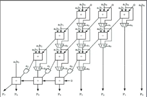
B. Column-Bypassing Multiplier
A column-bypassing multiplier is an advanced multiplier when compared to the traditional Array Multiplier (AM). A low power column-bypassing multiplier design is proposed to reduce power
and delay as well. According to Column Bypasing Multiplier [11]
the FA operations are disabled with the corresponding bit in the
multiplicand is 0. Fig. 4 shows the architecture of 4×4
column-bypassing multiplier. In open literature the column-column-bypassing
multiplier is available [12] it is given by M.C.Wen, et al.
Fig. 4: Column Bypassing Multiplier
C. Row-Bypassing Multiplier
A low-power row-bypassing multiplier [13] is also proposed to
reduce the activity power of the AM. The internal Architecture
of the Row bypassing multiplier is as shown in the fig. 5. The
operation of the low-power row-bypassing multiplier is nearer as that of the low-power column-bypassing multiplier, but the difference is the selector of the multiplexers and the tristate gates. The inputs are bypassed to FAs in the second rows, and the tristate gates turn off the input paths to the FAs. Therefore, no switching
activities occur in the first-row FAs; in return, power consumption is reduced. Similarly, because b2 is 0, no switching activities will
occur in the second-row FAs. However, the FAs must be active in
the third row because the b3 is not zero. More detailed information
for the row-bypassing multiplier is given in the open literature
[12] by J.Ohban etal.
III. Aging Aware Multiplier
The aging-aware reliable multiplier is the technique to implement
the FFT is designed by interlinking the Adaptive Hold Technique to the either Row-bypassing or Column- bypassing multipliers. The AHT [1] Architecture consists of different blocks such as of
two m-bit inputs (m is a positive number), one 2m-bit output, one
column or row-bypassing multiplier, 2m 1-bit Razor flip-flops, and
an AHT circuit. The overall architecture of the Aging Multiplier
is as shown in fig. 6.
Fig. 6: Architecture of Aging Aware Multiplier
The AHT architecture is power efficient and it can also adjust
the percentage of one-cycle patterns to minimize performance degradations due to the aging effect. When the circuit is aged,
and many errors occur, the AHT circuit uses the second judging block to decide if an input is one cycle or two cycles and hence the
timing errors can also be eliminated and can perform the error free
operations. The proposed AHT architecture [3-9] which is used
to design multiplier has a great advantage in the both Power and Delay as well and hence, it can be stated as the reliable multiplier technique which can be used in harsh environment mostly in aerospace applications etc.
IV. Fast Fourier Transform (FFT)
Fast Fourier Transform (FFT) is used to convert a signal from
domain to frequency & this is needed so that you can view the
frequency components present in the signals. A Fourier Transform converts a wave in the time domain to the frequency domain. An FFT is an algorithm that speeds up the calculation of a DFT.
The 4 input butterfly FFT is shown as in fig. 2. The complete 4 point FFT has 4 input and output values, where as the stage 1 has W base 2, stage 2 has W base 4 and their powers are 0 and 1 respectively. The input values are in reverse bit ordering. The Fig. 7 shows the 4- point FFT
Fig. 7: 4 Point Butterfly Structure FFT
Here are the equations derived from the 4 Point FFT
For stage 1:
For stage 2:
Substituting the stage 1 equations in stage 2, then the final FFT
expression is given as,
V. Experimental Results
Our experiments are conducted in a Windows operating system.
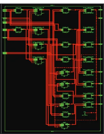
The design of the various multipliers along with the proposed Multiplier are synthesized and simulated, and their synthesized results are tabulated and compared. Figure – shows the RTL schematic for the FFT using one of the aging aware multiplier
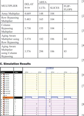
Technique. Table 1 is filled with the synthesis reports of the 4 bit
multipliers and the Table 2 is given with the DIT-FFT synthesis reports.
The implementation of DIT-FFT using traditional multipliers and the aging aware multiplier are also done using Verilog HDL in
Xilinx14.1, and the simulations are observed with ISE simulator. Xilinx Synthesizer is used to analyse the delay.
A. RTL Schematic of the Row Bypassing AHT Multiplier
B. Tabular Forms
Table 1: Comparison Table for 4 bit Multipliers
MULTIPLIER DELAY (ns) LUTS IO Buffers
Array Multiplier 15.339 30 16
Row Bypassing 14.709 36 16
Column Bypassing 13.283 28 16
Aging Aware Multiplier using
Row Bypassing 6.387 58 19
Aging Aware Multiplier using
Column Bypassing 6.387 64 19
Table 2: Comparisons of 4 Point DIT-FFT With Different
Multiplication Technique
MULTIPLIER DELAY in ns AREA
LUTs SLICES FLIP-FLOPS
Array Multiplier 4.669 148 104
-Row Bypassing
Multiplier 5.483 165 104
-Column Bypassing
Multiplier 5.730 155 104 -Aging Aware
Multiplier using
Row Bypassing 3.574 182 106 64
Aging Aware Multiplier
using Column Bypassing
3.576 298 106 85
C. Simulation Results
Fig. 8: Simulation Results for 4 Point DIT-FFT using Aging Aware (Row Bypassing Multiplier)
VI. Future Scope
The implementation of radix-2, 4 point DIT-FFT is done using Verilog HDL, as a future scope 8 point, 16 point, etc. DIT-FFTs
can be implemented with the help of the aging aware multiplier
to get high speed and power efficient devices.
VII. Conclusion
In this paper the implementation of high speed FFT is designed to reduce the delay. The FFT which is implemented using the AHT technique where as the AHT Multiplier has three important features. First, its Delay is very less when compared to the other
Traditional Multipliers. Second, it can provide reliable operations even after the aging effect occurs. The Razor flip-flops detect the
timing violations and reexecute the operations using two cycles.
Last but not least, the AHT architecture is power efficient and it can also adjust the percentage of one-cycle patterns to minimize
performance degradations due to the aging effect. When the circuit is aged, and many errors occur, the AHT circuit uses the second
judging block to decide if an input is one cycle or two cycles and
hence the timing errors can also be eliminated and can perform the error free operations. The proposed FFT is implemented using AHT architecture in its multiplication process has a great advantage in terms of Delay and hence, Adaptive Hold Technique can be stated as the reliable multiplier technique which can be used in FFTs in harsh environment mostly in aerospace applications etc.
References
[1] Lin, I.-C.; Cho, Y.-H.; Yang, Y.-M.,“Aging-Aware Reliable Multiplier Design With Adaptive Hold Logic,” Very Large Scale Integration (VLSI) Systems, IEEE Transactions on , Vol. PP, No. 99, pp. 1,1, March 2015.
[2] Yuke Wang ; YiyanTang ; Yingtao Jiang,"Novel memory
reference reduction methods for FFT implementations on
DSP processors”, IEEE Transactions on Signal Processing, Vol. 55, No. 5, pp. 2338- 2349, May 2007.
[3] Olivieri, N.,“Design of synchronous and asynchronous variable-latency pipelined multipliers,” Very Large Scale Integration (VLSI) Systems, IEEE Transactions on, Vol. 9, No. 2, pp. 365-376, April 2001.
[4] Calimera,A.; Macii, E.; Poncino, M.,“Design Techniques for NBTI Tolerant Power-Gating Architectures,” Circuits and Systems II: Express Briefs, IEEE Transactions on, Vol. 59, No. 4, pp. 249-253, April 2012.
[5] Paul, B.C., Kunhyuk Kang; Kufluoglu, H.; Alam, M.A.; Roy, K.,“Impact of NBTI on the temporal performance degradation of digital circuits,” Electron Device Letters, IEEE, Vol. 26, No. 8, pp. 560-562, Aug. 2005
[6] S.Zafar, A. Kumar, E. Gusev, E. Cartier,“Threshold voltage instabilities in high-k gate dielectric stack,” IEEE Trans. Device Mater. Rel., Vol. 5, No. 1, pp. 45–64, Mar. 2005. [7] B.C.Paul, K.Kang, H.Kufluoglu, M.A.Alam, K.Roy,
“Negative bias temperature instability: Estimation and design for improved reliability of nanoscale circuit,” IEEE Trans. Comput.-Aided Des. Integr. Circuits Syst., Vol. 26, No. 4, pp. 743–751, Apr. 2007.
[8] K.-C. Wu, D. Marculescu,“Aging-aware timing analysis and optimization considering path sensitization,” In Proc., 2011, pp. 1–6.
[9] Y. Lee, T. Kim,“A fine-grained technique of NBTI-aware
voltage scaling and body biasing for standard cell based
designs,” In Proc. ASPDAC, 2011, pp. 603–608.
[10] D. Mohapatra, G. Karakonstantis, K. Roy,“Low-power
process variation tolerant arithmetic units using input-based
elastic clocking,” In Proc. ACM/IEEE ISLPED, Aug. 2007, pp. 74–79.
[11] M.C. Wen, S.J. Wang, Y.N. Lin,“Low power parallel multiplier with column bypassing,” In Proc. IEEE ISCAS, May 2005, pp. 1638–1641.
P. Abhishek T S received B.Tech degree in Electronics and Co-mmunication Enginee-ring in the year 2012 from JNTU Kakinada and Pursuing M.Tech in VLSI at MVGR college of Engineering (Autonomous) affiliated to JNTU Kakinada.
Shaik Mastan Vali received his Ph.D from Andhra University in 2013. He is working as Professor in the Depa-rtment of Electronics Co-mmunication Engineer-ing at MVGR College of
Engineering (Autonomous). He has