Comparative Study of Millimeter-Wave
and THz Performance of DDR IMPATTs
Based on Group IV-IV and Group III-V
Materials
S.J.Mukhopadhyay
Department of E &TC, Indian Institute of Engineering Science and Technology, Shibpur, Howrah, West Bengal 711103, India
M.Mitra
Department of E &TC, Indian Institute of Engineering Science and Technology, Shibpur, Howrah, West Bengal 711103, India
Abstract: In this paper a comparative study has been made on IMPATT diodes based on group IV-IV materials such as Si, SiC(4H) and group III-V materials such as GaN(Wz), InP operating at Millimeter-wave(mm-wave) and Terahertz(THz)frequency. A double iterative computer method based on drift-diffusion model has been used to study the DC and small signal admittance properties of the device and corresponding avalanche response times as well as transit times are calculated. The simulation studies show that 4H-SiC based IMPATTs from group IV-IV are found to be excellent source for generation of RF power output at mm wave and THz frequency. It is also observed that GaN(Wz) based IMPATTs from group III-V are highly suitable for operation at higher order of THz frequency due to smaller value of avalanche response time. The RF power output for 4H-SiC is found to be 37.08 W and 8.25W for mm-wave and THz frequency respectively. The Avalanche response time of 0.78x10⁻¹⁵s and 0.54x10⁻¹⁶s is obtained for 4H-SiC and Wz-GaN based IMPATTs at THz frequency respectively.
Keywords: Si,4H-SiC,Wz-GaN,InP,Double drift IMPATT diode, RF power, Negative resistance, Avalanche response time, Transit time, MM-wave, Terahertz.
1. Introduction
Among all the solid state sources, IMPATT (impact avalanche transit time) devices have already emerged as high power, high-efficiency solid state sources for both microwave (3-30GHz) and millimeter-wave (30-300GHz)frequency bands. Nowadays Terahertz sources are in great demand for various application areas such as spectroscopy [Grischkowsky, 1990], biosensing [Debus, 2007], quality inspection in various industrial branches[Yasui,2005], medical and pharmaceutical applications [Fitzgerald,2005], THz astronomy[Siegel,2007],etc. The inherent advantages and potential benefits of the THz frequency regime (0.3-10THz) for both civilian and defence applications have generated lot of research interest in the development of THz components, source and detectors.
It is well known that RF power depends on various factors like critical field for avalanche breakdown, saturation drift velocity for charge carriers etc which varies for different semiconductor materials and play vital role in limiting the output power of an IMPATT diode at a particular operating frequency.
The rapid development of Silicon technology in the decade of seventies has made possible the practical realization of Silicon based single drift (SDR) and double drift (DDR) IMPATT devices capable of providing RF output power of the order of several watts at microwave and millimeter wave frequency bands[Midford and Bernick,1979-Ghosal,2011]. In the year of 1996,[Eisele et al,1996] first experimentally reported the InP-based IMPATTT operation at W band.
literature [Mukherjee and Majumder,2007].Here in this present paper, the authors have studied the millimeter-wave and THz performance of Si,4H-SiC,InP and Wz-GaN based DDR IMPATTs using an avalanche response time based analysis[Acharyya and Banerjee,2012 and 2013] following a double-iterative field maximum simulation method[Roy et. al,1979 and 1985] based on Gummel-Blue[Gummel and Blue,1967] model to obtain the upper cut-off frequencies for IMPATT operation.
2. Material Parameters and Design Method 2.1 Material Parameters
The electric field variation of carrier ionization rates in Si is given by αn,p(ζ)=An,pexp[(-Bn,p/ζ)m]
Where the value of constant m=1 for Si and InP and Wz-GaN. The values of An,p and Bn,p for Si have been taken from the experimental results[ Grant, 1973].The ionization coefficients An,p and Bn,p in InP have been obtained from the experimental data[Kao and Crowell, 1980] for lower field range(2.5*107 to 5.0*107 V/m) and Umebu et al.in 1980 for the higher field range(5.0*107 to 8.0*107 V/m).The same co-efficients (An,p and Bn,p) of Wz-GaN are taken from recently published report [Kunihiro et. al.,1999].
The field variation of carrier ionization rates in 4H-SiC is given by αn(ζ)=(ζ/An)exp(-Bn/ζ2) αp(ζ)=(ζ/7)exp[-1/(Apζ2+Bpζ)]
The values of constants An,p and Bn,p for a wide field range in 4H-SiC are taken from experimentally reported data[Konstantinov et.al.,1997].The electron and hole drift velocity versus field characteristics of Si have an experimental field dependence given b
vn,p(ζ)=vsn,sp[1-exp(-µn,pζ/vsn,sp)]
The values of vsn and vsp are taken from the experimental data [Canali et. al.,1971].The negative differential mobility in the electron drift velocity versus electric field characteristics of group III-V semiconductors InP[Kramer and Micrea,1975]and Wz-GaN[Shiyu and Wang ,2008]have been taken in the computer simulation method which incorporates a peak in the drift velocity at low field followed by a velocity saturation at high electric field. The hole drift velocity versus field characteristic of InP and Wz-GaN are same as Si.The field dependence of electron and hole drift velocity in 4H-SiC are given by [Vassilevski, 2001]:
vn,p(ζ)=[µn,pζ/(1+(µn,pζ/vsn,sp)k)]1/k
Where the value of k=1.20. All other material parameters such as bandgap(Eg), intrinsic carrier concentration(ni), effective density of states of conduction and valance bands(Nc,Nv), diffusion coefficients(Dn,Dp), mobilities(µn,µp) and diffusion lengths(Ln,Lp) of charge carriers and permittivity(ɛs) of the semiconductor materials under consideration are taken from published reports Electronic Archive[Electronic Archive,2012].
2.2Design-Method
Table 1. Structural and Doping Parameters at 94GHz
Base material
Design frequency fd (GHz)
Wn (µm)
Wp (µm)
ND
(x1023m-3) NA
(x1023m-3) Nsub (x1026m-3)
Si 94 0.390 0.390 1.20 1.25 1.0
4H-SiC 94 0.610 0.610 2.80 2.90 1.0
Wz-GaN 94 1.380 1.380 0.58 0.59 1.0
InP 94 0.339 0.339 1.60 1.60 1.0
Table 2. Structural and Doping Parameters at 0.5THz
Base material
Design frequency fd (THz)
Wn (µm)
Wp (µm)
ND
(x1023m-3) NA
(x1023m-3)
Nsub (x1026m-3)
Si 0.5 0.074 0.072 15.00 16.20 1.0
4H-SiC 0.5 0.180 0.180 14.50 16.50 1.0
Wz-GaN 0.5 0.330 0.330 2.80 2.90 1.0
InP 0.5 0.068 0.068 13.5 13.5 1.0
3. Proposed Analysis Model
One-dimensional model of reverse biased n+-n-p-p+ lateral DDR IMPATT structure, shown in Fig. 1 is used to simulate the DC and high frequency properties of the device. The physical phenomena take place in the semiconductor bulk along the symmetry axis of the DDR IMPATT devices. Thus the one-dimensional model of IMPATT devices considered in this work is justified
Fig 1. One-dimensional model of DDR IMPATTdevice.
DC Simulation
The DC electric field and normalized current density profiles in the depletion layer of the device are obtained from simultaneous numerical solution of fundamental device equations such as Poisson’s equation, combined carrier continuity equation, current density equations and mobile space charge equation subject to appropriate boundary conditions [ACharyya and Banerjee, 2012]. The simulation method starts with DC analysis described in details elsewhere [Roy et al,1985]. In this method, the computation starts from the field maximum near the metallurgical junction. The distribution of DC electric field and carrier currents in the depletion layer is obtained by the double-iterative computer method, which involves iteration over the magnitude of field maximum (Em) and its location in the depletion layer. A computer algorithm has been developed for simultaneous numerical solution of Poisson’s equation, carrier continuity equations and the space charge equation taking into account the effect of mobile space charge and carrier diffusion in order to obtain the electric field profiles and carrier current profiles. The boundary conditions for the electric field at the depletion layer edges are given by
x
1
0
and
x
2
0
(1)Where –x1 and x2 define the p+ and n+ edges of the depletion layer. Similarly the boundary conditions for normalized difference of hole and electron current density, P(x) = (Jp(x) – Jn(x)) / J0 (where J0 = Jp + Jn) at the depletion layer edges i.e., at x = -x1 and x = x2 are given by:
P(-x1)=(2/Mp-1) and P(x2)=(1-2/Mn) (2)
The conversion efficiency is calculated from the approximate formula [Eisele and Haddad,1997]
η(%)=(1*Vd)/(π*VB) (3)
Vd=Voltage drop across the drift region and VB=Breakdown voltage. Avalanche breakdown occurs in the junction when the electric field is large enough such that the charge multiplication factors(Mn,Mp)become infinite. Again breakdown voltage and avalanche zone voltage drop are calculated by integrating the spatial field profile over the total depletion layer width(W) and by integrating the spatial field profile over the total avalanche layer width(xA),respectively,i.e,
VB= and VA=
(4)
Where –x1=n-side depletion layer width and x2=p-side depletion layer width similarly –xA1= n-side avalanche layer width and xA2=p-side avalanche layer width.
Calculation of Avalanche Response Time
The avalanche response time of DDR IMPATTs can be calculated from the knowledge of static spatial distribution of electron and hole ionization rates (αn(x) vs. x and αp(x) vs. x) obtained from DC simulation, saturated drift velocities of charge carriers(vsn and vsp).If ƬAn and ƬAp are the avalanche response times initiate by electrons and holes, respectively, then these are expressed as [Acharyya and Banerjee,2012 and 2013]:
(5)
(6) When avalanche process is initiated by a mixture of electrons and holes then the corresponding response time ƬA is given by [Acharyya and Banerjee,2013].
(7)
Where the parameter k=Jps/Js and (1-k)= Jns/Js;
Js= Jps+ Jns is the total reverse saturation current of the device under dark condition. The expression for thermally generated electron and hole reverse saturation currents are given by
Jns=[qDnni2/LnNA] and Jps=[qDpni2/LpND]. (8) High-frequency Simulation
resistance (ZR) and reactance (ZX) are obtained from the numerical integration of the respective R(x)- and X(x)-profiles over the depletion layer width (W), i.e.:
2 1 x xR R x dx
Z and
2 1 x
x
X X x dx
Z (9)
The device impedance is given by, ZD = ZR + jZX while the device admittance is, YD = ZD-1 = G + jB. The negative conductance (G) and susceptance (B) of the device at a particular frequency are computed from the following expressions:
-G=-ZR/[(ZR)2+(ZX)2] and B=ZX/[(ZR)2+(ZX)2] (10)
It may be noted that both -G and B are normalized with respect to the junction area (Aj) of the device. The avalanche frequency (fa) is the frequency at which the imaginary part (B) of the admittance changes its nature from inductive to capacitive. Again it is the minimum frequency at which the real part (G) of admittance becomes negative and oscillation starts to build up in the circuit.
At a resonant frequency of oscillation, the maximum power output PRF from the device can be obtained from the following expression,
PRF=V2RF(Gp)Aj/2 (11)
Where,VRF is the amplitude of the RF swing and is taken as VB/2,assuming 50% modulation of the breakdown voltage VB. Gp is the diode negative conductance at the operating frequency and Aj is the junction area of the diode.
4. Results and Discussions DC Properties
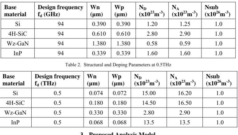
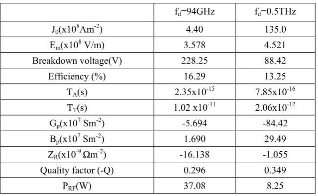
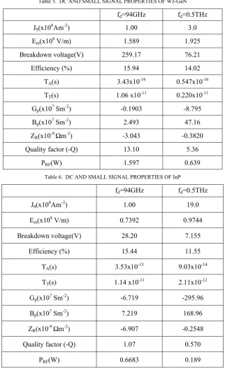
Important DC parameters as peak electric field (ζp),break down voltage(VB),avalanche zone voltage(VA),DC to RF conversion efficiency of the designed DDR IMPATTs are obtained from DC simulation. The comparison of DC properties of DDR IMPATTs based on different semiconductors can be made from Table 3, 4, 5 and 6 at different operating frequency. It is observed that peak electric field (ζp) at the junction increases while the breakdown voltage(VB), DC to RF conversion efficiency decrease in the DDR IMPATTs based on different materials as the operating frequency changes to terahertz regime. Fig.2 and fig.4 turns out that Peak electric field (ζp)is highest in 4H-SiC based DDRs from group IV-IV among all other DDR IMPATTs under consideration at any operating frequency, it increases from 3.57x10⁸ to 4.52x10⁸Vm-1 as the operating frequency increases from 94GHz to 0.5THz.In Wz-GaN based DDR IMPATTs from group III-V,Peak electric field (ζp)is of the same order(~108Vm-1) but lower than 4H-SiC DDRs as shown in Fig.6 and 8.It is observed that Si and InP based DDRs have lower breakdown voltage (VB) than either 4H-SiC or Wz-GaN based DDRs at any operating frequency. It is interesting to observe that maximum breakdown voltage (VB) of 259V obtained in Wz-GaN based IMPATT at mm-wave(94GHz)whereas for 4H-SiC based DDR IMPATTs provide highest breakdown voltage of 88V at THz. Considering the DC parameter in terms of efficiency, It may be observed that 4H-SiC based IMPATTs from IV-IV group and Wz-GaN based IMPATTs from III-V group perform better than others at any operating frequency. In mm-wave, 4H-SiC based DDR IMPATTs provide highest conversion efficiency (~16%) whereas in THz, Wz-GaN based DDR IMPATTs provide highest DC to RF conversion efficiency(~14%).
Avalanche response times
High-frequency properties
The important high frequency parameters obtained from the analysis are optimum frequency(fp), peak negative conductance(Gp),corresponding susceptance(Bp),quality factor or Q-factor(Qp),negative resistance(ZR) and RF power output(PRF).Those parameters are obtained from the high frequency simulation of Si,4H-SiC,Wz-GaN and InP IMPATTs are listed in Tables below. It is observed that magnitude of ZR is highest in 4H-SiC based DDR among all other devices at any operating frequency. Higher magnitude of negative resistance implies that higher RF power output can be obtained from 4H-SiC based DDR IMPATT devices in comparison with Si, InP and Wz-GaN based DDR IMPATT operating at same design frequency. It is interesting to note that Wz-GaN and 4H-SiC DDR IMPATTs are potential candidates for THz operation due to their higher RF power output comparative to all other devices under consideration. Table below shows that PRF decreases as the operating frequency increases from mm-wave (94GHz) to THz (0.5THz). In addition to this it is also observed from Table 5 below that Wz-GaN based diodes perform superior than others in terms of quality factor at any operating frequency. The Q-factor determines the growth rate and stability of oscillation. Less Q-factor means better device performance. The admittance characteristics or high frequency conductance-susceptance plots for mm-wave and THz of Si,4H-SiC,Wz-GaN and Inp IMPATTs are shown in fig3,5,7 and 9.It is observed that the magnitudes of Gp and Bp increase with increase of operating frequency from mm-wave to THz.
Table 3. DC AND SMALL SIGNAL PROPERTIES OF Si
fd=94GHz fd=0.5THz
J0(x108Am-2) 3.40 52.0
Em(x108 V/m) 0.6012 1.216
Breakdown voltage(V) 24.310 8.93
Efficiency (%) 10.678 4.25
ƬA(s) 1.92x10⁻¹² 6.13x10⁻¹³
ƬT(s) 1.06 x10⁻¹¹ 1.89x10⁻¹²
Gp(x107 Sm-2) -4.3344 -68.129
Bp(x107 Sm-2) 6.4804 253.05
ZR(x10-9 Ωm-2) -7.1309 -0.0992
Quality factor (-Q) 1.4950 3.71
PRF(W) 0.3202 0.0678
Table 4. DC AND SMALL SIGNAL PROPERTIES OF 4H-SiC
fd=94GHz fd=0.5THz
J0(x108Am-2) 4.40 135.0
Em(x108 V/m) 3.578 4.521
Breakdown voltage(V) 228.25 88.42
Efficiency (%) 16.29 13.25
ƬA(s) 2.35x10⁻¹⁵ 7.85x10⁻¹⁶
ƬT(s) 1.02 x10⁻¹¹ 2.06x10⁻¹²
Gp(x107 Sm-2) -5.694 -84.42
Bp(x107 Sm-2) 1.690 29.49
ZR(x10-9 Ωm-2) -16.138 -1.055
Quality factor (-Q) 0.296 0.349
Table 5. DC AND SMALL SIGNAL PROPERTIES OF Wz-GaN
fd=94GHz fd=0.5THz
J0(x108Am-2) 1.00 3.0
Em(x108 V/m) 1.589 1.925
Breakdown voltage(V) 259.17 76.21
Efficiency (%) 15.94 14.02
ƬA(s) 3.43x10⁻¹⁶ 0.547x10⁻¹⁶
ƬT(s) 1.06 x10⁻¹¹ 0.220x10⁻¹¹
Gp(x107 Sm-2) -0.1903 -8.795
Bp(x107 Sm-2) 2.493 47.16
ZR(x10-9 Ωm-2) -3.043 -0.3820
Quality factor (-Q) 13.10 5.36
PRF(W) 1.597 0.639
Table 6. DC AND SMALL SIGNAL PROPERTIES OF InP
fd=94GHz fd=0.5THz
J0(x108Am-2) 1.00 19.0
Em(x108 V/m) 0.7392 0.9744
Breakdown voltage(V) 28.20 7.155
Efficiency (%) 15.44 11.55
ƬA(s) 3.53x10⁻¹³ 9.03x10⁻¹⁴
ƬT(s) 1.14 x10⁻¹¹ 2.11x10⁻¹²
Gp(x107 Sm-2) -6.719 -295.96
Bp(x107 Sm-2) 7.219 168.96
ZR(x10-9 Ωm-2) -6.907 -0.2548
Quality factor (-Q) 1.07 0.570
Fig2.Electric field profile for Si and 4H-SiC DDR IMPATT at MM-wave Fig3.High-freq plot for Si and 4H-SiC DDR IMPATT at MM
Fig6.Electric field profile for Wz-GaN and InP DDR IMPATT at MM Fig7.High-freq plot for Wz-GaN and InP DDR IMPATT at MM
Fig8.Electric field profile for Wz-GaN and InP DDR IMPATT at THz Fig9.High-freq plot for Wz-GaN and InP DDR IMPATT at THz
5. Conclusions
Millimeter-wave and Terahertz performance of DDR IMPATT devices based on group IV-IV and III-V are investigated in this paper. The simulation experiment demonstrates the suitability of using SiC(4H) from group IV-IV and GaN(Wz) from group III-V for fabrication of high frequency electronic devices due to their small avalanche response time, high DC to RF conversion efficiency and sufficiently high RF power output as compared to Si, InP based IMPATTs. The investigation also revealed that SiC(4H) IMPATT diodes give superior performance in terms of output RF power at mm-wave and THz compared to IMPATT diodes fabricated from Si,GaN(Wz) and InP. The simulation results and corresponding designs would be useful for undertaking an experimental program to fabricate the THz 4H-SiC and Wz-GaN based IMPATTs.
Acknowledgment
References
[1] Grischkowsky, D.; Keiding, S.;Exter, M.;Fattinger, C., “Far-infrared time-domain spectroscopy with terahertz beams of dielectrics and
semiconductors”,.J Opt Soc Am B 7:2006-2015,1990.
[2] Debus, C,;Bolivar ,PH., “Frequency selective surfaces for high sensitivity terahertz sensing”,Appl Phys Lett 91:184102,2007.
[3] Yasui, T.; Yasuda, T.; Sawanaka, K.;Araki T , “Terahertz paintmeter for noncontact monitoring of thickness and dying progress in
paint flim”,Appl Opt 44:6849- 6856,2005.
[4] Fitzgerald AJ, Cole BE, Taday PF, “Nondestructive analysis of tablet coating thickness using terahertz pulsed imaging”,J Pharm Sci
94:177-183,2005.
[5] Siegel PH , “THz Instruments for Space”,IEEE Trans Antenn Propag 55:2957–2965,2007.
[6] Midford T. A. and Bernick R. L., “Millimeter -wave CW IMPATT diodes and Oscillators”, IEEE Trans. Microwave Theory Tech., 27,
483 (1979).
[7] Chang Y., Hellum J. M., Paul J. A. and Weller K. P., “Millimeter-wave IMPATT Sources for Communication Applications”, IEEE
MTT-S International Microwave Symposium Digest, 216-219 (1977).
[8] Gray W. W., Kikushima L., Morentc N. P. and Wagner R. J., “Applying IMPATT Power Sources to Modern Microwave Systems”.
IEEE Journal of Solid-State Circuits, 4, 409-413 (1969).
[9] Ghoshal D., “Measurement of electrical resistance of Silicon Single Drift Region IMPATT diode based on the study of the device and
mounting circuit at threshold condition”, Journal of Electron Devices, 11, 625-631 (2011).
[10] Eisele H,Chen CC,Munns GO,Haddad GI, “The Potential of InP IMPATT diodes as high-power millimeter-wave sources:first
experimental results. IEEE MTT-S Int Microwave Symp Digest 2:529-532” (1996).
[11] Mukherjee M,Majumder N “Effects of charge bump on high frequency characteristics of α-SiC based double drift ATT diodes at
millimeter wave window frequencies”,IETE Journal of research,vol-55,issue 3,118-126.
[12] Acharyya, A., Banerjee, J. P., “Potentiality of IMPATT devices as terahertz source: an avalanche response time based approach to
determine the upper cut-off frequency limits”, IETE J Res59, 2013.
[13] Acharyya, A., Banerjee, S., Banerjee, J. P., “Calculation of avalanche response time for determining the high frequency performance
limitations of IMPATT devices”,J Electron Dev 12:756-760,2012.
[14] Roy, S. K., Sridharan, M., Ghosh, R., Pal, B. B. “ Computer methods for the dc field and carrier current profiles in impatt devices
starting from the field extremum in the depletion layer”, Proc. of NASECODE-I Conf. on Numerical Analysis of Semiconductor Devices (Dublin: Boole Press), 1979, p. 266-274.
[15] Roy, S. K., Banerjee, J. P., Pati, S. P. “A computer analysis of the distribution of high frequency negative resistance in the depletion
layers of impatt diodes”.,Proc. of NASECODE-IV Conf. on Numerical Analysis of Semiconductor Devices (Dublin: Boole Press), 1985, p. 494-500.
[16] Gummel, H. K., Blue, J. L. “ A small-signal theory of avalanche noise in IMPATT diodes”.,IEEE Trans. on Electron Devices, 1967,
vol. 14, no. 9, p. 569-580.
[17] Grant WN, “Electron and hole ionization rates in epitaxial silicon-solid state Electron ”,16:1189-1203,1973.
[18] Kao CW,Crowell CR, “Impact ionization by electrons and holes in InP”, Solid state Electron 23:881-891.
[19] Kunihiro K,Kasahara K,Takahashi Y,Ohno Y, “Experimental evalution of impact ionization coefficients in GaN”. IEEE Electron
Device Lett 20:608-610.
[20] Konstantinov AO,Wahab Q,Nordell N, Lindefelt U, “Ionization rates and critical fields in 4H-Silicon Carbide.”, Appl Phys Lett
71:90-92,1997.
[21] Canali C,Ottaviani G.Quaranta AA, “Drift velocity of electrons and holesand associated anisotropic effects in Silicon.”,J Phys Chem
Solids 32:1707,1971.
[22] Kramer B,Micrea A, “Determination of saturated electron velocity in GaAs”,Appl Phys Lett 26:623-624.
[23] Shiyu SC,Wang G, “High-field properties of carrier transport in bulk wurtzite GaN”,:monte Carlo perspective.J Appl Phys
103:703-708.
[24] Vassilevski KV,Zorenko AV,Zekentes k,Tsagaraki K,Bano E,Banc C,Lebedev A, “4H-SiC IMPATT diode fabrication and testing.
”In:technical digest of international conference on SiC and related materials,Tsukuba,Japan,pp 713-714.
[25] Electronic Archive(2012) New semiconductor Materials, Characteristics and Properties. http;//www.ioffe.ru/SVA/NSM/semicond.
[26] Sze, S. M., Ryder, R. M. Microwave Avalanche Diodes. Proc. of IEEE, Special Issue on Microwave Semiconductor Devices, 1971,
vol. 59, no. 8, p. 1140-1154
[27] Acharyya, A., Banerjee, J. P., “Analysis of Photo-Irradiated Double-Drift Region Silicon Impact Avalanche Transit Time Devices in
the Millimeter-wave and Terahertz Regime”, Terahertz Science and Technology, 2012, vol. 5, no. 2, p. 97-113.