University of New Hampshire
University of New Hampshire Scholars' Repository
Space Science Center
Institute for the Study of Earth, Oceans, and Space
(EOS)
3-10-2003
Development of CZT strip detector modules for
0.05- to 1-MeV gamma-ray imaging and
spectroscopy
James M. Ryan
University of New Hampshire, [email protected]
B Donmez
University of New Hampshire - Main Campus
John R. Macri
University of New Hampshire - Main Campus, [email protected]
M McClish
University of New Hampshire - Main Campus
Mark L. McConnell
University of New Hampshire - Main Campus, [email protected]
See next page for additional authors
Follow this and additional works at:
https://scholars.unh.edu/ssc
Part of the
Astrophysics and Astronomy Commons
This Conference Proceeding is brought to you for free and open access by the Institute for the Study of Earth, Oceans, and Space (EOS) at University of New Hampshire Scholars' Repository. It has been accepted for inclusion in Space Science Center by an authorized administrator of University of New Hampshire Scholars' Repository. For more information, please [email protected].
Recommended Citation
Authors
Development of CZT Strip Detector Modules for 0.05 to 1 MeV
Gamma-Ray Imaging and Spectroscopy
J. M. Ryan
*a, B. Donmez
a, J. R. Macri
a, M. McClish
a, M. L. McConnell
a, R. S. Miller
a,
M. Widholm
a, L.-A. Hamel
b, M. Julien
ba
Space Science Center, University of New Hampshire, Durham, NH 03824 USA
b
Physics Department, University of Montreal, Montreal, Quebec, Canada
ABSTRACT
We report progress in our study of cadmium zinc telluride (CZT) strip detectors featuring orthogonal coplanar anode contacts. We specifically report on the performance, characterization and stability of 5 and 10 mm thick prototype CZT detectors fabricated using material from several manufacturers. Our ongoing work includes laboratory and simulation studies aimed at optimizing and developing compact, efficient, high performance detector modules for 0.05 to 1 MeV gamma radiation measurements with space-based instrumentation. The coplanar anode strip configuration retains many of the performance advantages of pixel detectors yet requires far fewer electronic channels to perform both 3-d imaging and spectroscopy. Minimizing the channel count is important for large balloon or space instruments including coded aperture telescopes (such as MARGIE or EXIST) and Compton imaging telescopes (such as TIGRE or ACT). We also present plans for developing compact, space qualified imaging modules designed for integration into closely packed large area detector arrays. We discuss issues associated with detector module and array electronics design and development.
Keywords: CdZnTe, CZT, gamma-ray, imaging, spectroscopy
1. INTRODUCTION
The Energetic X-ray Imaging Survey Telescope (EXIST) is a wide field-of-view, coded aperture telescope for observations in the 10 to 600 keV energy range. The Advanced Compton Telescope (ACT) is an instrument concept to study 0.3 to 10 MeV gamma rays with spectral and angular resolution significantly improved over the instruments of the CGRO and INTEGRAL missions.1, 2The baseline detector plane for EXIST calls for 8 m2of 10 mm thick CZT pixel detectors with pixel pitch of 1.2 mm. ACT will require similar large area imaging detector arrays. The detection areas are necessary to meet mission sensitivity goals, while the detector must be thick to meet the upper end of the energy range with reasonable efficiency.
Because of its high stopping power and demonstrated excellent room temperature spectroscopic and imaging capabilities, CZT is an attractive candidate detector material for these instruments. The cost (~$3000/cm3), however, for material of sufficient quality is currently prohibitive for large area applications. We are hopeful that efforts to significantly improve the yields from the material growth process will be successful, thereby lowering costs. Meanwhile, other important technical development issues such as detector design and fabrication, front-end electronics and array packaging are being addressed.
Aselectron-onlydevices, CZT detectors, patterned with small pixels, effectively mitigate the problems associated with poor hole transport observed in CZT. Pixel detectors with thicknesses up to 10 mm have been demonstrated to perform well as efficient imagers and spectrometers3,4. Small pixel anode electrodes patterned onto CZT material have lower capacitance and leakage current than any other contact geometry. As such they represent the best performance approach for both spectroscopy and imaging. Furthermore, the energy deposits and locations of multi-hits from Compton events within the same CZT substrate can be detected and measured unambiguously. The principle deficiency with pixel detectors is that they require an electronic readout channel for each pixel, a significant disadvantage in space-based
*
Correspondence:E-mail: [email protected] telephone: 603-862-3510; fax: 603-862-3584
X-Ray and Gamma-Ray Telescopes and Instruments for Astronomy, Joachim E. Trümper, Harvey D. Tananbaum, Editors, Proceedings of SPIE Vol. 4851 (2003)
© 2003 SPIE · 0277-786X/03/$15.00
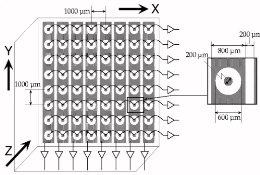
Figure 1. Contact geometry and read out of the orthogonal coplanar anode design. Strip columns (X) are read out on the bottom. Pixel rows (Y) are read out on the right. The gold contact pattern dimensions shown here in grey correspond to those of our prototype assemblies. On the right is the fundamental unit we call a pixel.
instruments requiring large area detector arrays. We have rather focused on the development of orthogonal strip detectors. The advantage of orthogonal strip detectors over pixel detectors in such large detector arrays is greatly reduced channel count. Fewer channels draw less power, reduce the complexity of the instrument electronics and lead to more tractable thermal control solutions. An 8 m2array of 1.2 mm pixels implies 5.5 million signal channels, or 5.5 kW at 1 mW per channel. The same area array of 16¥16 orthogonal strip detector modules requires one eighth the number of channels and consumes proportionally less power.
Double-sided CZT strip detectors, if carefully designed, can address much of the limitation associated with poor hole transport.5 Due to this limitation, however, there will always be an upper limit on detector thickness (~3 mm) and thus the effective energy range (<300 keV). Double-sided strip detectors require that signals be processed from the strip contacts on both surfaces. The wiring associated with these contacts adds to dead area in closely packed arrays of imaging modules. To address these problems and to explore new fabrication technologies we have been developing a novel CZT detector concept: anelectron-onlydevice featuringorthogonal coplanar anode strips. This detector concept, and the performance of 5 and 10 mm thick prototypes, are described below.
Aside from the cost and availability of adequate quality CZT material, issues related to further development of these detectors for space applications include: optimizing the detector geometry; defining the front-end electronics, developing and integrating compact, low power integrated readout circuits; and compact packaging. Detector geometry optimization involves both laboratory studies and simulations of charge transport and signal generation as reported previously.6 In addition, Monte Carlo studies are necessary to assign energy and spatial resolution requirements to various instrument applications and to study the effects of off-axis incidence and multi-hits.
2. THE ORTHOGONAL COPLANAR ANODE STRIP DETECTOR
Figure 1 illustrates the anode surface contact pattern and the readout of an 8¥8 orthogonal coplanar anode strip detector. As with double-sided strip detectors, this detector requires simultaneous readout of both row and column signals. Each row takes the form of N discrete interconnected anode pixel electrodes while each column is a single strip electrode. We use the termpixelto refer to either the smallest
electrode or to the region defined by the intersection of a row and column (Figure 1). The opposite surface, not shown, has a single uniform cathode electrode. The anode pixel contacts, interconnected in rows, are biased to collect the electron charge carriers. The orthogonal anode strips, surrounding the anode pixel electrodes, are biased between the cathode and anode pixel potentials. The strips register signals induced by the motion of electrons as they migrate to the pixels. Since electrons are much more mobile than holes in CZT, anode signals from photon interactions at all depths in the detector are detected, whereas with double-sided detectors hole trapping attenuates or quenches any cathode signal. This permits thicker, more efficient CZT imaging planes than are practical with double-sided strip detectors, and extends the effective energy range to >1 MeV. In addition more compact packaging is possible since all imaging contacts
3. ASSEMBLY OF PROTOTYPE MODULES
Our prototype module assemblies involve the application of two key technologies: Low Temperature Cofired Ceramics (LTCC) and Polymer Flip-Chip (PFC) bonding.6, 7 Figure 2 (left) is a photograph of prototype components: a patterned CZT substrate (left) and its mating LTCC carrier. Its assembly involves electrical and mechanical PFC bonding between the two surfaces shown in the photograph. Figure 2 (right) shows conducting epoxy bumps stenciled onto the 200 µm diameter pixels in preparation for the PFC bonding.
Figure 2. Detector prototype components (left): a patterned CZT substrate (left) and its mating ceramic (LTCC) carrier. The light-colored areas on the surfaces are gold contacts. Conducting epoxy bumps (right)
There are 8 rows of 8 gold contact pads on the LTCC substrate corresponding to the pixels on the CZT anode. There is a ninth row of 8 pads making contact with the strips. A large contact pad in one corner connects the cathode bias. The interconnection of the pixels in rows and a breakout of the detector contact elements to pins in a standard pin grid array (PGA) pattern is on the underside of the LTCC substrate (not shown).
PFC bonding was used to form the electrical and mechanical connection of the patterned CZT and LTCC substrates of our prototype detector assemblies. The PFC bonding technique uses silver-filled conductive epoxy to electrically connect the contacts of electronic components. Conducting polymer bumps (~120 µm diameter, ~20 µm high) are stencil printed and can be cured at temperatures as low as room temperature (Figure 2, right). Similar conducting bumps are stenciled on the mating LTCC substrates. The bumped surfaces are aligned and mated while one set of conducting bumps is still wet, then cured.
A non-conducting epoxy underfill is then used to fill all voids between the mating surfaces and around the conducting bumps to provide mechanical strength. All processing steps take place below 80˚C, well below the 100°C maximum recommended by CZT material manufacturers. Once the assembly is cured the rugged LTCC substrate can be used for all handling of the detector. The conducting bump and underfill materials are mechanically compliant and thus aid in reducing the mechanical stress to the CZT as well as providing thermal insulation. The result is a rugged assembly that involves no wire bonds to the CZT anode surface (Figure 3). Once set up, this bonding process is fully automated and produces highly reliable interconnections at low incremental cost. PFC bonding is used in other applications to reliably interconnect pads as small as 75 µm with pitch as fine as 125 µm. The first 5 mm thick prototype detectors were assembled in 1999. Tests at that time included thermal cycle and random vibration of one module. Additional prototypes, including 10 mm thick detectors, were assembled in 2001. We have observed no degradation in their spectroscopic performance (Section 4.2). Table 1 lists the prototype detector modules discussed below.
Table 1. Detector Prototypes thickness Material
Manufacturer
Assembly Date
UNH ID#
5 mm eV Products June 1999 UNH-EV-3 5 mm eV Products June 1999 UNH-EV-4 5 mm Yinnel Tech. Dec, 2001 UNH-Y-5 10 mm eV Products Dec, 2001 UNH-EV-11 10 mm Yinnel Tech. Dec, 2001 UNH-Y-2
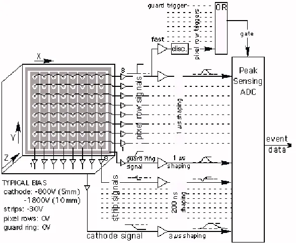
Figure 4. Laboratory setup.
4. PROTOTYPE PERFORMANCE
4.1 Measurement Setup
Figure 4 shows the signal processing setup employed for the study of the 8¥8 prototype detectors. The detectors were plugged into a custom test board for bias and readout of the charge signals with discrete preamplifiers (eV-5093). The signal processing and data acquisition used NIM, CAMAC and VME electronics. Typical bias levels for the
electrodes are shown for each detector thickness. Each charge collecting pixel row signal was split into a fast and a shaped channel. The fast pixel row channels were used to trigger event data acquisition. Any pixel row (or the guard ring) signal above its discriminator level will gate the peak sensing ADC. The peak level of 18 shaped signals (8 pixel rows, 8 orthogonal strips, cathode and guard ring) was recorded for each triggered event.
Pixel row signals, generated from the collection of carrier electrons on the smallest electrodes, were used as the event trigger because they provide the best signal to noise ratio. These signals were also used to determine the energy and the Y -coordinate of the photon interaction location. The guard ring is biased and its signals were processed like the pixel rows to maintain a uniform electric field and to identify photon interactions occurring outside the 8¥8 mm2 imaging area.
The strip signals were used to measure the
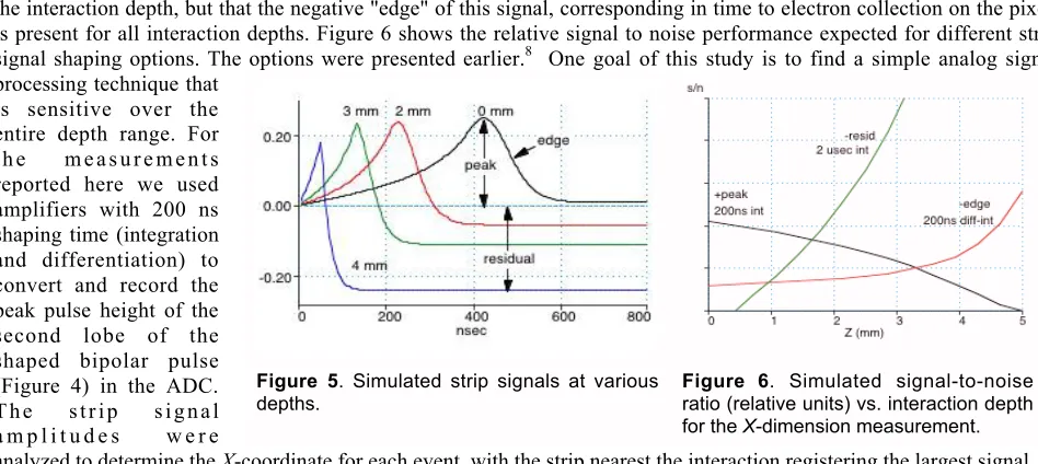
X-coordinate of the photon interactions. The strip signal is generally bipolar and ranges in amplitude between 25% and 40% of the pixel signal. Ideally, the strips collect no charge, but, due to their size and proximity to the pixels, register the motion of charge in the detector and, specifically, of electrons as they are collected on the pixels. Figure 5 shows simulated strip
Figure 5. Simulated strip signals at various depths.
Figure 6. Simulated signal-to-noise ratio (relative units) vs. interaction depth for the X-dimension measurement.
signals for several interaction depths in a 5 mm thick detector. Note that the strip signal shape changes significantly with the interaction depth, but that the negative "edge" of this signal, corresponding in time to electron collection on the pixel, is present for all interaction depths. Figure 6 shows the relative signal to noise performance expected for different strip signal shaping options. The options were presented earlier.8 One goal of this study is to find a simple analog signal processing technique that
is sensitive over the entire depth range. For t h e m e a s u r e m e n t s reported here we used amplifiers with 200 ns shaping time (integration and differentiation) to convert and record the peak pulse height of the second lobe of the shaped bipolar pulse (Figure 4) in the ADC. T h e s t r i p s i g n a l a m p l i t u d e s w e r e
analyzed to determine the X-coordinate for each event, with the strip nearest the interaction registering the largest signal.
We are pursuing approaches for measuring theZ-coordinate of interactions without a cathode signal. In an earlier paper we presented the first measurements of a design that employed a time-over-threshold circuit on the leading lobe of the strip signal.9 Another option is to sum all anode signals, strips and pixels. This sum would be equivalent to, albeit noisier than, the cathode signal. The interaction depth (Z) is presently inferred from the ratio of the cathode to largest pixel amplitude, and, with calibration constants specific to the setup, is computed using (1-cathode/pixel)¥L, whereL
is the detector thickness.
4.2 Spectroscopy
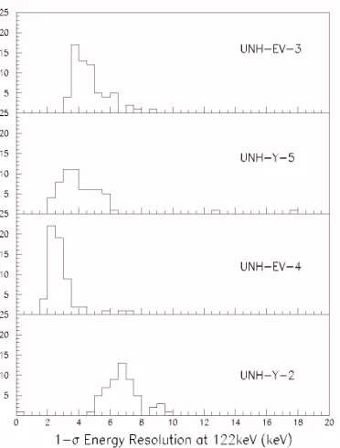
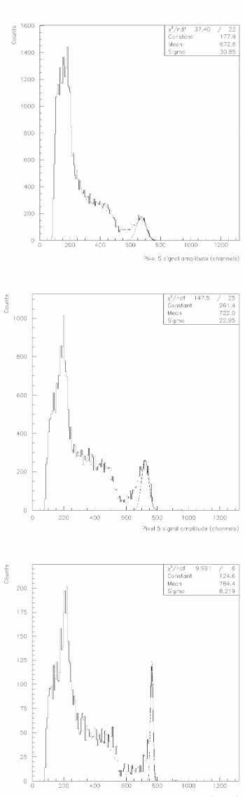
Figure 7 shows the response to 122 and 136 keV photons from a 57Co source measured in July 2002 with one of our original 5 mm thick detectors (UNH-EV-3). The detector was made with discriminator-grade single-crystal material from eV Products. Sixty-four spectra are shown sorted by the pixel row and strip column registering the maximum signal for each triggered event in the 8¥8 patterned detector. Note that the 122 and 136 keV peaks are clearly resolved in most pixels. Figure 8 shows the energy resolution distribution for these pixels (UNH-EV-3, top panel) as determined from the 1-swidth of a Gaussian fit to the 122 keV peak. The remaining histograms in Figure 8 show the distributions of energy resolution for all pixels with two other 5 mm detectors and one 10 mm thick detector. Note that only 56 pixels are included in the histogram for 10 mm thick detector UNH-Y-2 as one pixel row channel (8 pixels) was too noisy to measure. No correction for electron trapping was made here. This effect can be significant, especially for the 10 mm thick detector.
A single pixel response to photons in the energy range from 14 to 662 keV is shown in Figure 9. These data were collected in June 2002 using detector UNH-EV-4. This performance is similar to that recorded in the initial testing of this detector.10
The response to 662 keV photons from a137Cs source of 10 mm thick detector UNH-EV-11 is shown in Figure 10. The effect of electron trapping across the 10 mm thickness is evident in the photopeak pulse height as measured for different interaction depths (Z). The best energy resolution (2.5% FWHM) is measured for events occurring near the anode plane. In addition to the effects of electron trapping we have observed that a significant amount of charge is actually collected on the strips of 10 mm thick detector UNH-EV-11. This is not the case with our 5 mm thick detectors. Preliminary measurements indicate that 30% of events have more than 10% charge collection by the strip and that 15% of events have more than 50% charge collection by the strip. Further study is planned to better understand this effect. Since charge collected on the pixels is the measure of energy, this effect degrades spectroscopic performance. The charge collected on the strips has two other consequences: 1) it attenuates the pixel signal for some events dropping them below the trigger
threshold resulting in a loss of efficiency and 2) it changes the nature of the induced signal on the strips thus degrading the spatial resolution in the X-coordinate.
1 2 3 4 5 6 7 8
1 2 3 4 5 6 7 8
Strip (Column)
Pi
xe
l(
Ro
w
)
Figure 7. Energy spectra of individual pixels collected with 5 mm thick detector UNH-EV-3. Energy scale is 0–150 keV
57
Co photopeaks are at 122 and 136 keV. Event location is determined by identifying the maximum pixel and maximum strip signal for each trigger.
4.3 Efficiency
The detection efficiencies were measured for a 5 mm and a 10 mm thick detector (UNH-EV-3 and UNH-EV-11) and compared to predictions. With the discriminator threshold set at 100 keV, triggered events at two energies (122 and 662 keV) were counted and compared to the total expected, given the source activity, distance and exposure time, in
the imaging volume (8¥8¥thickness mm3). Table 2 summarizes the results. At 122 keV we find good agreement between measurement and theory for the 5 mm detector. We attribute the lower than expected response of the 10 mm detector to two factors both of which reduce the number of triggered events: 1) electron trapping reducing the signal amplitude for events near the cathode causing some of these to fall below the trigger threshold and 2) a significant fraction of the electrons are collected on the strips for events occurring under the corners of the unit cell (pixel) with this detector. At 662 keV we suspect that the higher than expected number of detections is due to Compton scattering from passive material surrounding the detector. Further study is planned to better assess the efficiency of our detectors.
4.4 Imaging
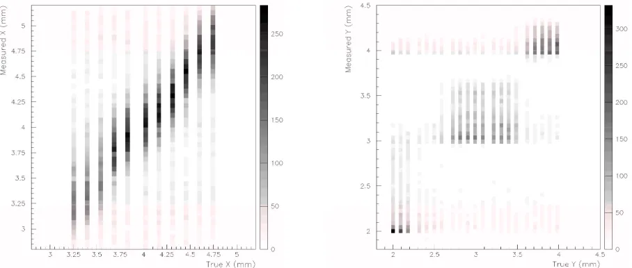
We used a tungsten collimator with a 200 µm diameter bore hole and 241Am and 57Co point sources to measure the capability for determining theXandYlocations of photon interactions. Figure 11 shows the result of 122 keV photon
Table 2. Summary of Efficiency Measurements
122 keV 662 keV
detector thickness
measured (%)
expected (%)
measured (%)
expected (%)
Figure 8.Energy resolution distribution at 122 keV for the 64 pixels of four prototype detectors (56 pixels are shown for UNH-Y-2, bottom panel).
Figure 9. Single "pixel" response across the energy range from 14 to 662 keV with 5 mm thick detector UNH-EV-4. Calibration sources: 241Am (top), 57Co (center),
137
Cs (bottom)
beam-spot scans performed in 150 µm steps in each dimension with 5 mm thick detector (UNH-EV-3). Sub-pitch (sub-mm) locations are computed by interpolation of the pulse height data of neighboring channels. This works well in the strip (X) dimension. The discontinuity between true and measured location inYindicates that there is very little charge sharing between pixel rows.
Figure 12 shows 2-d histograms of computed event locations (X,Y) in response to beam spot illuminations of this detector with 122 keV (left) and 60 keV (right) photons. The beam spot diameter is ~0.2 mm. The measured spatial resolutions (FWHM) are 0.6 mm (X) and 0.5 mm (Y) at 122 keV and 1.0 mm (X) and 0.4 mm (Y) at 60 keV. Additional signal to noise improvements of the strip signal circuitry are necessary to extend the threshold for measuring location in the X-dimension to lower energies.
Sub-mm spatial resolution at 122 keV in the Z dimension was previously demonstrated with 5 mm thick detector UNH-EV-4.6 The ratio of cathode and pixel pulse heights was used to compute the Z coordinate.
5. DETECTOR MODULE CONCEPT FOR
LARGE-AREA ARRAYS
The baseline approach for packaging an imaging module is shown in Figure 13. A complete imaging module consists of a patterned CZT substrate that has been PFC bonded to a ceramic (LTCC) substrate or multi chip module (MCM).
Figure 10. 10 mm thick detector UNH-EV-11 response to 662 keV photons at different interaction depths: Z=0-4.5 mm (top), 4.5-9 mm (middle), and 9-10 mm (bottom).
Here we envision a module with 16¥16 pixels formed from 16 strips and 16 pixel rows, each on a 1 mm pitch. The CZT substrate in this case is roughly 16¥16 mm2.
The PFC bonding process provides the mechanical and electrical interconnection between the CZT and LTCC substrates. The multi-layer LTCC substrate provides the interconnection of the anode pixels in rows and the routing of the pixel row and strip signals (total of 32) to flat gold contact pads on the underside of the module. Mechanical support for handling the module and aligning and mounting it to the image plane is integral to the LTCC substrate. The fact that 256 pixels are present with only 32 signal processing channels leaves ample space on the underside of the LTCC substrate for the passive components (resistors and capacitors) necessary for the ac-coupled strip signals and for the mounting hardware. Similarly, the limited number of channels permits ample space on the underside of the image plane board for each module’s FEE ASICs within the module footprint.
This modular concept has several important advantages:
• The rugged, compact design makes for easy handling and mounting of the CZT detectors.
• The CZT detector is thermally isolated from the heat-generating electronics by the LTCC substrate and the PFC bonding layer.
• There is a clean separation between the passive and active components of the detection system without the need for long leads that not only take up space, but also add capacitance and noise.
• There can be a clean separation of the detector and front end electronics development efforts, without requiring costly and risky disassembly and re-assembly operations.
• Modules are 4-side buttable on large area image plane boards.6
6. CONCLUSIONS AND FUTURE WORK
prototype detectors and have demonstrated stable performance of detector modules
assembled more than three years ago. We have conducted preliminary efficiency measurements and demonstrated full efficiency of a 5 mm thick detector at 122 keV.
Figure 12. Image of 122 keV beam spot (left) and 60 keV beam spot (right)
Further laboratory study is needed here to understand discrepancies in these efficiency measurements at higher energies and with the 10 mm detectors. Further laboratory study is also planned to better understand and resolve the problem of partial charge collection on the strip electrodes.
Together with additional laboratory measurements of the currently available detectors, we will use our charge transport and signal generation simulation tools to optimize designs for new prototype detectors. We plan to fabricate new
Figure 11. Photon beam spot scans illustrate position determination capabilities at 122 keV in X (left) and Y (right) dimensions. Collimated 57Co beam diameter is 200 µm. Scan step is 150 µm. 5 mm thick detector.
Figure 13. Concept for a detector module to be used in fabrication of large area arrays
detector module prototypes and begin testing them with application specific integrated circuitry (ASIC). This will lead directly to the development of a suitable ASIC design, which will, in turn, will lead to the fabrication of an engineering model detector module based on the packaging concept presented in Figure 13. We will also perform detailed Monte Carlo studies to fully characterize the physics of high energy photon interactions in CZT.
REFERENCES
1. Recommended Priorities for NASA’s Gamma-Ray Astronomy Program, NASA Gamma-Ray Program Working Group (GRAPWG), NASA 1999.
2. Astronomy and Astrophysics in the New Millennium, Astronomy and Astrophysics Survey Committee, Board on Physics and Astronomy, Space Studies Board, National Research Council 2001.
3. Z. He, W. Li, G. F. Knoll, D. K. Wehe, J. Berry, and C. M. Stahle, “3-D position sensitive CdZnTe gamma-ray spectrometers,”NIMA422, pp. 173-178, 1999.
4 A. Shor, I. Mardor, and Y.Eisen, "Performance of 1cm¥1cm¥1cm Pixelated CdZnTe Gamma Detectors," Conference Record, IEEE Nuclear Science Symposium, Nov. 2001.
5. J. L. Matteson, F. Duttweiler, G. L. Huszar, P. C. Leblanc, R. E. Skelton, E. A. Stephan, P. L. Hink, P. F. Dowkontt, K. R. Slavis, T. O. Tumer, and S. D. Kavis, “Position-sensitive CZT detector module,” Proc. SPIE3446, pp 192-201, 1998.
6. M. L. McConnell, J. R. Macri, J. M. Ryan, K. Larson, L.-A. Hamel, G. Bernard, C. Pomerleau, O. Tousignant, J.-C. Leroux, V. Jordanov, "Three-dimensional imaging and detection efficiency performance of orthogonal coplanar CZT strip detectors," Proc. SPIE,4141, 157, 2000.
7. V. T. Jordanov, J. R. Macri, J. E. Clayton, and K. A. Larson, “Multi-Electrode CZT Detector Packaging Using Polymer Flip Chip Bondin," 11th International Workshop on Room Temperature Semiconductor X- and Gamma-Ray Detectors and Associated Electronics, Vienna, Austria, October 1999, to be published in NIM A.
8. J. R. Macri, P. Dufour, L. A. Hamel, M. Julien, M. L. McConnell, M. McClish, J. M. Ryan, M. Widholm, "Study of 5 and 10 mm Thick CZT Strip Detectors," Conference Record, IEEE Nuclear Science Symposium, Nov. 2001.
9. K. Larson, V. Jordanov, M. L. McConnell, J. R. Macri, J. M. Ryan, L.-A., Hamel, and O. Tousignant, “Analog Processing of Signals from a CZT Strip Detector with Orthogonal Coplanar Anodes,” in Proc. SPIE4141, 2000. 10. O. Tousignant, L. A. Hamel, P. Dufor, F. Joly, J. R. Macri, M. L. McConnell, J. M. Ryan, and V. T. Jordanov,